 | –≠–ª–µ–∫—Ç—Ä–æ–Ω–Ω—ã–π –∫–æ–º–ø–æ–Ω–µ–Ω—Ç: 24C160-SN | –°–∫–∞—á–∞—Ç—å:  PDF PDF  ZIP ZIP |
©
1996 Microchip Technology Inc.
Preliminary
DS21147F-page 1
FEATURES
∑ SPI modes 0,0 and 1,1
∑ 3 MHz Clock Rate
∑ Single 5V supply
∑ Low Power CMOS Technology
- Max Write Current: 5 mA
- Read Current: 1.0 mA
- Standby Current: 1
µ
A typical
∑ Organization
- 1024 x 8 for 25C080
- 2048 x 8 for 25C160
∑ 16 Byte Page
∑ Self-timed ERASE and WRITE Cycles
∑ Sequential Read
∑ Block Write Protection
- Protect none, 1/4, 1/2, or all of Array
∑ Built-in Write Protection
- Power On/Off Data Protection Circuitry
- Write Latch
- Write Protect Pin
∑ High Reliability
- Endurance: 10M cycles (guaranteed)
- Data Retention: >200 years
- ESD protection: >4000 V
∑ 8-pin PDIP/SOIC Packages
∑ Temperature ranges supported
DESCRIPTION
The Microchip Technology Inc. 25C080/160 are 8K and
16K bit Serial Electrically Erasable PROMs. The mem-
ory is accessed via a simple Serial Peripheral Interface
(SPI) compatible serial bus. The bus signals required
are a clock input (SCK) plus separate data in (SI) and
data out (SO) lines. Access to the device is controlled
through a chip select (CS) input, allowing any number
of devices to share the same bus.
There are two other inputs that provide the end user
with additional flexibility. Communication to the device
can be paused via the hold pin (HOLD). While the
device is paused, transitions on its inputs will be
ignored, with the exception of chip select, allowing the
host to service higher priority interrupts. Also write
operations to the Status Register can be disabled via
the write protect pin (WP).
- Commercial (C):
0
∞
C to
+70
∞
C
- Industrial (I):
-40
∞
C to
+85
∞
C
- Automotive (E):
-40∞C to +125∞C
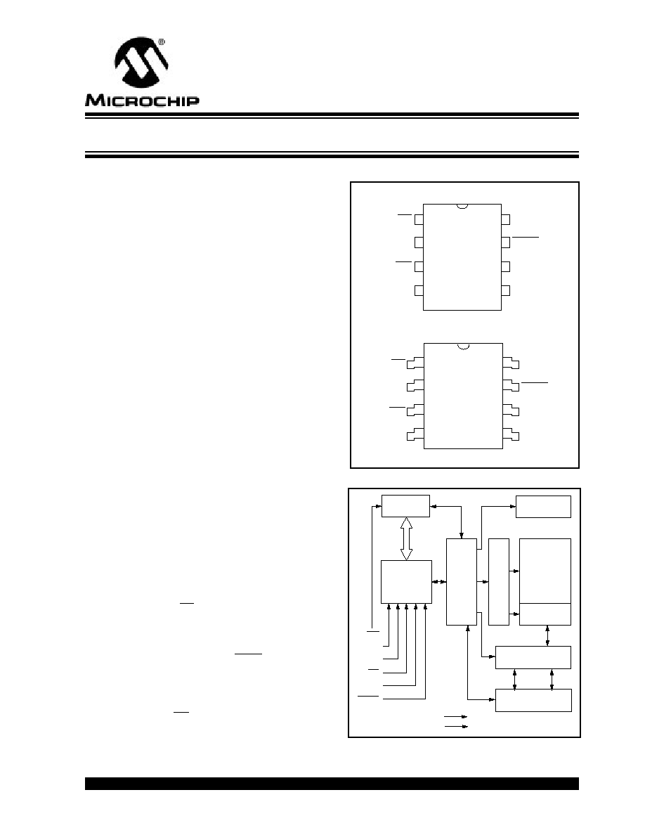
PACKAGE TYPES
BLOCK DIAGRAM
25C080/16
0
CS
SO
WP
V
SS
1
2
3
4
8
7
6
5
V
CC
HOLD
SCK
SI
25C080/160
CS
SO
WP
V
SS
1
2
3
4
8
7
6
5
V
CC
HOLD
SCK
SI
PDIP
SOIC
SI
SO
SCK
CS
HOLD
WP
Status
Register
I/O Control
Memory
Control
Logic
X
Dec
HV Generator
EEPROM
Array
Page Latches
Y Decoder
Sense Amp.
R/W Control
Logic
Vcc
Vss
25C080/160
8K/16K 5.0V SPI
TM
Bus Serial EEPROM
SPI is a trademark of Motorola.
This document was created with FrameMaker 4 0 4
25C080/160
DS21147F-page 2
Preliminary
©
1996 Microchip Technology Inc.
1.0
ELECTRICAL
CHARACTERISTICS
1.1
Maximum Ratings*
V
CC
........................................................................ 7.0V
All inputs and outputs w.r.t. V
SS
...... -0.6V to V
CC
+1.0V
Storage temperature .............................-65∞C to 150∞C
Ambient temperature under bias ...........-65∞C to 125∞C
Soldering temperature of leads (10 seconds) ...+300∞C
ESD protection on all pins...................................... 4kV
*Stresses above those listed under `Maximum ratings' may
cause permanent damage to the device. This is a stress rating
only and functional operation of the device at those or any
other conditions above those indicated in the operational list-
ings of this specification is not implied. Exposure to maximum
rating conditions for extended period of time may affect device
reliability
TABLE 1-1:
PIN FUNCTION TABLE
Name
Function
CS
Chip Select Input
SO
Serial Data Output
SI
Serial Data Input
SCK
Serial Clock Input
WP
Write Protect Pin
V
SS
Ground
V
CC
Supply Voltage
HOLD
Hold Input
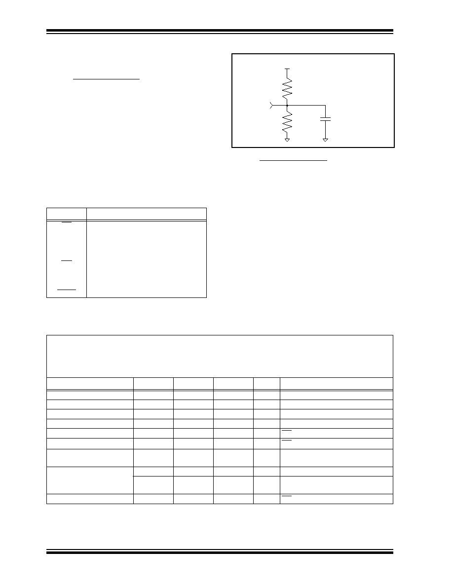
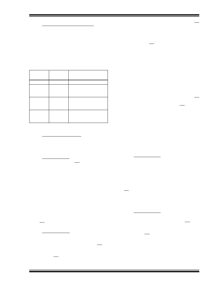
FIGURE 1-1:
AC TEST CIRCUIT
1.2
AC Test Conditions
AC Waveform:
V
LO
= 0.2V
V
HI
= Vcc - 0.2V
(Note 1)
V
HI
= 4.0V
(Note 2)
Timing Measurement Reference Level
Input
0.5 V
CC
Output
0.5 V
CC
Note 1: For V
CC
4.0V
2: For V
CC
> 4.0V
Vcc
SO
100 pF
1.8 K
2.25 K
TABLE 1-2:
DC CHARACTERISTICS
Applicable over recommended operating ranges shown below unless otherwise noted.
V
CC
= 4.5V to 5.5V
Commercial (C): Tamb = 0
∞
C to +70
∞
C
Industrial (I):
Tamb = -40
∞
C to +85
∞
C
Automotive (E): Tamb = -40∞C to +125∞C
Parameter
Symbol
Min
Max
Units
Test Conditions
High level input voltage
V
IH1
2.0
V
CC
+1
V
Low level input voltage
V
IL1
-0.3
0.8
V
Low level output voltage
V
OL
--
0.4
V
I
OL
=2.1 mA
High level output voltage
V
OH
V
CC
-0.5
--
V
I
OH
=-400
µ
A
Input leakage current
I
LI
-10
10
µ
A
CS=V
IH
, V
IN
=Vss to V
CC
Output leakage current
I
LO
-10
10
µ
A
CS=V
IH
, V
OUT
=Vss to V
CC
Internal Capacitance
(all inputs and outputs)
C
INT
--
7
pF
Tamb=25∞C, F
CLK
=3.0 MHz,
V
CC
=5.5V (Note)
Operating Current
ICC write
--
5
mA
V
CC
=5.5V
I
CC
READ
ICC
READ
--
--
1
500
mA
µ
A
V
CC
=5.5V; 3 MHz
V
CC
=5.5V; 2 MHz
Standby Current
I
CCS
--
5
µ
A
CS=V
CC
=5.5V; Vin=0V or V
CC
Note:
This parameter is periodically sampled and not 100% tested.

©
1996 Microchip Technology Inc.
Preliminary
DS21147F-page 3
25C080/160
FIGURE 1-2:
SERIAL INPUT TIMING
FIGURE 1-3:
SERIAL OUTPUT TIMING
FIGURE 1-4:
HOLD TIMING
CS
SCK
SI
SO
t
CSS
t
HD
t
SU
t
F
t
R
t
CSD
t
CLD
t
CSH
LSB in
MSB in
high impedance
CS
SCK
SO
t
LO
t
HI
t
HO
t
V
MSB out
LSB out
t
CSH
t
DIS
don't care
SI
CS
SCK
SO
SI
HOLD
t
HH
t
HS
t
HS
t
HH
t
HV
t
HZ
don't care
t
SU
high impedance
n+2
n+1
n
n-1
n
n+2
n+1
n
n
n-1
25C080/160
DS21147F-page 4
Preliminary
©
1996 Microchip Technology Inc.
TABLE 1-3:
AC CHARACTERISTICS
Applicable over recommended operating ranges shown below unless otherwise noted.
V
CC
= 4.5V to 5.5V
Commercial (C): Tamb = 0
∞
to +70
∞
C
Industrial (I):
Tamb = -40
∞
to +85
∞
C
Automotive (E): Tamb = -40∞C to +125∞C
Symbol
Parameter
Min
Max
Units
Test Conditions
f
SCK
Clock Frequency
--
3
MHz
t
CSS
CS Setup Time
100
--
ns
t
CSH
CS Hold Time
100
--
ns
t
CSD
CS Disable Time
250
--
ns
t
SU
Data Setup Time
30
--
ns
t
HD
Data Hold Time
50
--
ns
t
R
CLK Rise Time
--
2
µ
s
(Note 1)
t
F
CLK Fall Time
--
2
µ
s
(Note 1)
t
HI
Clock High Time
150
--
ns
t
LO
Clock Low Time
150
--
ns
t
CLD
Clock Delay Time
50
--
ns
t
V
Output Valid from
Clock Low
--
150
ns
t
HO
Output Hold Time
0
--
ns
t
DIS
Output Disable Time
--
200
ns
(Note 1)
t
HS
HOLD Setup Time
100
--
ns
t
HH
HOLD Hold Time
100
--
ns
t
HZ
HOLD Low to Output High-Z
100
--
ns
(Note 1)
t
HV
HOLD High to Output Valid
100
--
ns
(Note 1)
t
WC
Internal Write Cycle Time
--
5
ms
(Note 2)
--
Endurance
10M
--
E/W Cycles 25
∞
C, Vcc = 5.0V, Block Mode
(Note 3)
Note 1: This parameter is periodically sampled and not 100% tested.
2: t
WC
begins on the rising edge of CS after a valid write sequence and ends when the internal self-timed write
cycle is complete.
3: This parameter is not tested but guaranteed by characterization. For endurance estimates in a specific appli-
cation, please consult the Total Endurance Model which can be obtained on our BBS or website.

©
1996 Microchip Technology Inc.
Preliminary
DS21147F-page 5
25C080/160
2.0
PRINCIPLES OF OPERATION
The 25C080/160 is an 1024/2048 byte EEPROM
designed to interface directly with the Serial Peripheral
Interface (SPI) port of many of today's popular micro-
controller families, including Microchip's midrange
PIC16CXX microcontrollers. It may also interface with
microcontrollers that do not have a built-in SPI port by
using discrete I/O lines programmed properly with soft-
ware.
The 25C080/160 contains an 8-bit instruction register.
The part is accessed via the SI pin, with data being
clocked in on the rising edge of SCK. The CS pin must
be low and the HOLD pin must be high for the entire
operation. If the WPEN bit in the status register is set,
the WP pin must be held high to allow writing to the non-
volatile bits in the status register.
Table 2-1 contains a list of the possible instruction bytes
and format for device operation. All instructions,
addresses and data are transferred MSB first, LSB last.
Data is sampled on the first rising edge of SCK after CS
goes low. If the clock line is shared with other peripheral
devices on the SPI bus, the user can assert the HOLD
input and place the 25C080/160 in `HOLD' mode. After
releasing the HOLD pin, operation will resume from the
point when the HOLD was asserted.
2.1
Write Enable (WREN) and Write
Disable (WRDI)
The 25C080/160 contains a write enable latch. This
latch must be set before any write operation will be
completed internally. The WREN instruction will set the
latch, and the WRDI will reset the latch. The following is
a list of conditions under which the write enable latch
will be reset:
∑ Power-up
∑ WRDI instruction successfully executed
∑ WRSR instruction successfully executed
∑ WRITE instruction successfully executed
2.2
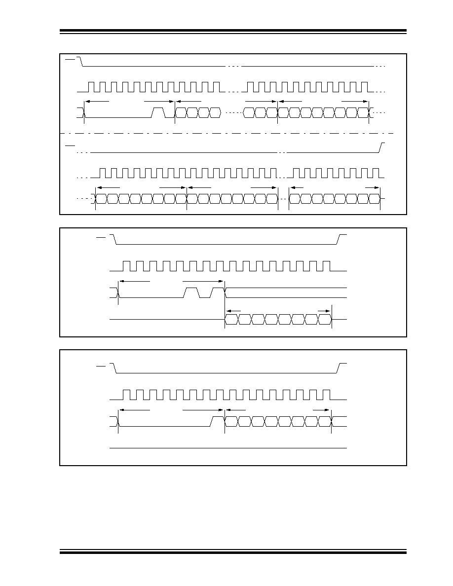
Read Status Register (RDSR)
The RDSR instruction provides access to the status
register. The status register may be read at any time,
even during a write cycle. The status register is format-
ted as follows:
The Write-In-Process (WIP) bit indicates whether the
25C080/160 is busy with a write operation. When set to
a `1' a write is in progress, when set to a `0' no write is
in progress. This bit is read only.
The Write Enable Latch (WEL) bit indicates the status
of the write enable latch. When set to a `1' the latch
allows writes to the array and status register, when set
to a `0' the latch prohibits writes to the array and status
register. The state of this bit can always be updated via
7
6
5
4
3
2
1
0
WPEN
X
X
X
BP1
BP0
WEL
WIP
the WREN or WRDI commands regardless of the state
of write protection on the status register. This bit is read
only.
The Block Protection (BP0 and BP1) bits indicate
which blocks are currently write protected. These bits
are set by the user issuing the WRSR instruction.
These bits are non-volatile.
The Write Protect Enable (WPEN) bit is a non-volatile
bit that is available as an enable bit for the WP pin. The
Write Protect (WP) pin and the Write Protect Enable
(WPEN) bit in the status register control the program-
mable hardware write protect feature. Hardware write
protection is enabled when WP pin is low and the
WPEN bit is high. Hardware write protection is disabled
when either the WP pin is high or the WPEN bit is low.
When the chip is hardware write protected, only writes
to non-volatile bits in the status register are disabled.
See Table 2-2 for matrix of functionality on the WPEN
bit and Figure 2-1 for a flowchart of Table 2-2. See
Figure 3-5 for RDSR timing sequence.
TABLE 2-1:
INSTRUCTION SET
Instruction
Name
Instruction
Format
Description
WREN
0000 0110 Set the write enable latch
(enable write operations)
WRDI
0000 0100 Reset the write enable
latch (disable write opera-
tions)
RDSR
0000 0101 Read status register
WRSR
0000 0001 Write status register (write
protect enable and block
write protection bits)
READ
0000 0011 Read data from memory
array beginning at
selected address
WRITE
0000 0010 Write data to memory
array beginning at
selected address
25C080/160
DS21147F-page 6
Preliminary
©
1996 Microchip Technology Inc.
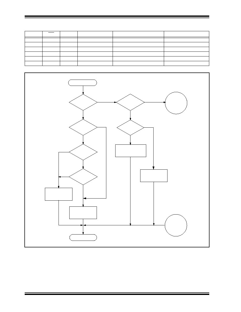
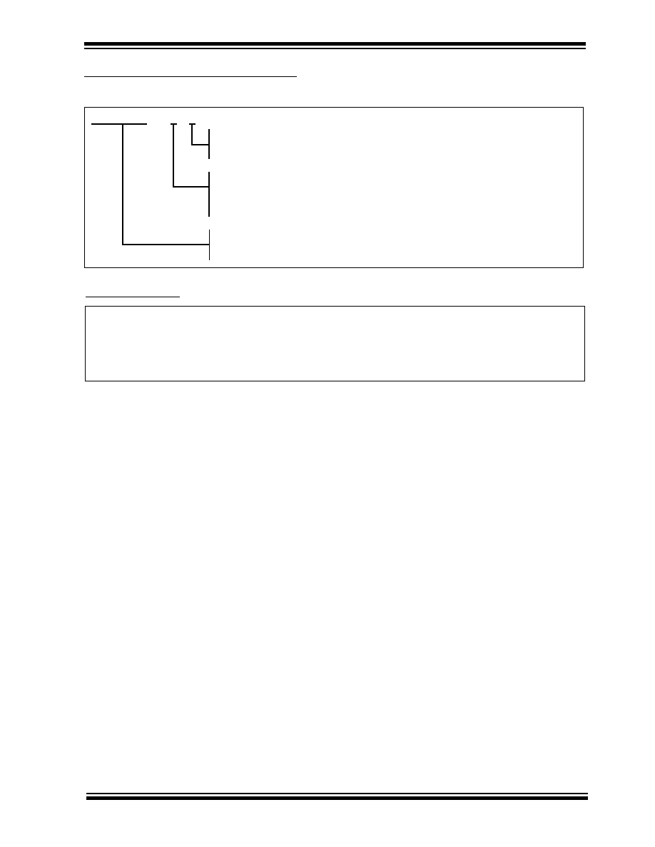
TABLE 2-2:
WRITE PROTECT FUNCTIONALITY MATRIX
FIGURE 2-1:
WRITE TO STATUS REGISTER AND/OR ARRAY FLOWCHART
WPEN
WP
WEL
Protected Blocks
Unprotected Blocks
Status Register
0
X
0
Protected
Protected
Protected
0
X
1
Protected
Writable
Writable
1
Low
0
Protected
Protected
Protected
1
Low
1
Protected
Writable
Protected
X
High
0
Protected
Protected
Protected
X
High
1
Protected
Writable
Writable
CS Returns High
Continue
WEL = 1?
WEL = 1?
WP is low?
WPEN = 1?
Write
Write to
Status Register
Do not write to
Status Register
Write to the
Unprotected Block
Do not write to
Array
No
No
No
No
Yes
Yes
Yes
Yes
No
Yes
No
Yes
To other
Commands
From other
Commands
Write
to Status
Reg?
to array?
©
1996 Microchip Technology Inc.
Preliminary
DS21147F-page 7
25C080/160
2.3
Write Status Register (WRSR)
The WRSR instruction allows the user to select one of
four protection options for the array by writing to the
appropriate bits in the status register. The array is
divided up into four segments. The user has the ability
to write protect none, one, two, or all four of the seg-
ments of the array. The partitioning is controlled as illus-
trated in table below. See Figure 3-6 for WRSR timing
sequence.
TABLE 2-3:
ARRAY PROTECTION
3.0
DEVICE OPERATION
3.1
Clock and Data Timing
Data input on the SI pin is latched on the rising edge of
SCK. Data is output on the SO pin after the falling edge
of SCK.
3.2
Read Sequence
The part is selected by pulling CS low. The 8-bit read
instruction is transmitted to the 25C080/160 followed by
the 16-bit address, with the five (25C160) or six
(25C080) MSBs of the address being don't care bits.
After the correct read instruction and address are sent,
the data stored in the memory at the selected address
is shifted out on the SO pin. The data stored in the
memory at the next address can be read sequentially
by continuing to provide clock pulses. The internal
address pointer is automatically incremented to the
next higher address after each byte of data is shifted
out. When the highest address is reached ($3FF for
25C080, $7FF for 25C160) the address counter rolls
over to address $000 allowing the read cycle to be con-
tinued indefinitely. The read operation is terminated by
setting CS high (see Figure 3-1).
3.3
Write Sequence
Prior to any attempt to write data to the 25C080/160,
the write enable latch must be set by issuing the WREN
instruction (Figure 3-2). This is done by setting CS low
and then clocking the proper instruction into the
25C080/160. After all eight bits of the instruction are
transmitted, the CS must be brought high to set the
write enable latch. If the write operation is initiated
BP1
BP0
Array Addresses
Write Protected
0
0
none
0
1
upper 1/4
300h-3FFh for 25C080
600h-7FFh for 25C160
1
0
upper 1/2
200h-3FFh for 25C080
400h-7FFh for 25C160
1
1
all
000h-3FFh for 25C080
000h-7FFh for 25C160
immediately after the WREN instruction without CS
being brought high, the data will not be written to the
array because the write enable latch will not have been
properly set.
Once the write enable latch is set, the user may pro-
ceed by setting the CS low, issuing a write instruction,
followed by the 16-bit address, with the five (25C160) or
six (25C080) MSBs of the address being don't care bits,
and then the data to be written. Up to 16 bytes of data
can be sent to the 25C080/160 before a write cycle is
necessary. The only restriction is that all of the bytes
must reside in the same page. A page address begins
with XXXX XXXX XXXX 0000 and ends with XXXX
XXXX XXXX 1111. If the internal address counter
reaches XXXX XXXX XXXX 1111 and the clock contin-
ues, the counter will roll back to the first address of the
page and overwrite any data in the page that may have
been written.
For the data to be actually written to the array, the CS
must be brought high after the least significant bit (D0)
of the n
th
data byte has been clocked in. If CS is brought
high at any other time, the write operation will not be
completed. See Figure 3-3 and Figure 3-4 for more
detailed illustrations on the byte write sequence and the
page write sequence, respectively.
While the write is in progress, the status register may
be read to check the status of the WPEN, WIP, WEL,
BP1, and BP0 bits. A read attempt of a memory array
location will not be possible during a write cycle. When
a write cycle is completed, the write enable latch is
reset
3.4
Data Protection
The following protection has been implemented to pre-
vent inadvertent writes to the array:
∑ The write enable latch is reset on power-up.
∑ A write enable instruction must be issued to set
the write enable latch.
∑ After a successful byte write, page write, or status
register write, the write enable latch is reset.
∑ CS must be set high after the proper number of
clock cycles to start an internal write cycle.
∑ Access to the array during an internal write cycle
is ignored and programming is continued.
3.5
Power On State
The 25C080/160 powers on in the following state:
∑ The device is in low power standby mode (CS=1).
∑ The write enable latch is reset.
∑ SO is in high impedance state.
∑ A low level on CS is required to enter active state.
25C080/160
DS21147F-page 8
Preliminary
©
1996 Microchip Technology Inc.
FIGURE 3-1:
READ SEQUENCE
FIGURE 3-2:
WRITE ENABLE SEQUENCE
FIGURE 3-3:
WRITE SEQUENCE
SO
SI
SCK
CS
0
2
3
4
5
6
7
8
9
10 11
21 22 23 24 25 26 27 28 29 30 31
1
0
1
0
0
0
0
0
1
15 14 13 12
2
1
0
7
6
5
4
3
2
1
0
instruction
16 bit address
data out
high impedance
SCK
0
2
3
4
5
6
7
1
SI
high impedance
SO
CS
0
1
0
0
0
0
0
1
SO
SI
CS
9 10 11
21 22 23 24 25 26 27 28 29 30 31
0
0
0
0
0
0
0
1
15 14 13 12
2
1
0
7
6
5
4
3
2
1
0
instruction
16 bit address
data byte
high impedance
SCK
0
2
3
4
5
6
7
1
8
T
wc
©
1996 Microchip Technology Inc.
Preliminary
DS21147F-page 9
25C080/160
FIGURE 3-4:
PAGE WRITE SEQUENCE
FIGURE 3-5:
READ STATUS REGISTER SEQUENCE
FIGURE 3-6:
WRITE STATUS REGISTER SEQUENCE
SI
CS
9 10 11
21 22 23 24 25 26 27 28 29 30 31
0
0
0
0
0
0
0
1
15 14 13 12
2
1
0
7
6
5
4
3
2
1
0
instruction
16 bit address
data byte 1
SCK
0
2
3
4
5
6
7
1
8
SI
CS
41 42 43
46 47
7
6
5
4
3
2
1
0
data byte n (16 max)
SCK
32
34 35 36 37 38 39
33
40
7
6
5
4
3
2
1
0
data byte 3
7
6
5
4
3
2
1
0
data byte 2
44 45
SO
SI
CS
9
10 11 12 13 14 15
1
1
0
0
0
0
0
0
7
6
5
4
2
1
0
instruction
data from status register
high impedance
SCK
0
2
3
4
5
6
7
1
8
3
SO
SI
CS
9
10 11
12 13 14 15
0
1
0
0
0
0
0
0
7
6
5
4
2
1
0
instruction
data to status register
high impedance
SCK
0
2
3
4
5
6
7
1
8
3

25C080/160
DS21147F-page 10
Preliminary
©
1996 Microchip Technology Inc.
4.0
PIN DESCRIPTIONS
4.1
Chip Select (CS)
A low level on this pin selects the device. A high level
deselects the device and forces it into standby mode.
However, a programming cycle which is already in
progress will be completed, regardless of the CS input
signal. If CS is brought high during a program cycle, the
device will go into standby mode as soon as the pro-
gramming cycle is complete. As soon as the device is
deselected, SO goes to the high impedance state,
allowing multiple parts to share the same SPI bus. A
low to high transition on CS after a valid write sequence
is what initiates an internal write cycle. After power-up,
a low level on CS is required prior to any sequence
being initiated.
4.2
Serial Input (SI)
The SI pin is used to transfer data into the device. It
receives instructions, addresses, and data to be written
to the memory. Input is latched on the rising edge of the
serial clock.
It is possible for the SI pin and the SO pin to be tied
together. With SI and SO tied together, two way com-
munication of data can occur using only one microcon-
troller I/O line.
4.3
Serial Output (SO)
The SO pin is used to transfer data serially out of the
25C080/160. During a read cycle, data is shifted out on
this pin after the falling edge of the serial clock.
It is possible for the SI pin and the SO pin to be tied
together. With SI and SO tied together, two way com-
munication of data can occur using only one microcon-
troller I/O line.
4.4
Serial Clock (SCK)
The SCK is used to synchronize the communication
between a master and the 25C080/160. Instructions,
addresses, or data present on the SI pin are latched on
the rising edge of the clock input, while data on the SO
pin is updated after the falling edge of the clock input.
4.5
Write Protect (WP)
This pin is used in conjunction with the WPEN bit in the
status register to prohibit writes to the non-volatile bits
in the status register. When WP is low and WPEN is
high, writing to the non-volatile bits in the status register
is disabled. All other operations function normally.
When WP is high, all functions, including writes to the
non-volatile bits in the status register operate normally.
If the WPEN bit is set WP low during a status register
write sequence will disable writing to the status register.
If an internal write cycle has already begun, WP going
low will have no effect on the write.
The WP pin function is blocked when the WPEN bit in
the status register is low. This allows the user to install
the 25C080/160 in a system with WP pin grounded and
still be able to write to the status register. The WP pin
functions will be enabled when the WPEN bit is set
high.
4.6
Hold (HOLD)
The HOLD pin is used to suspend transmission to the
25C080/160 while in the middle of a serial sequence
without having to re-transmit the entire sequence over
at a later time. It should be held high any time this func-
tion is not being used. Once the device is selected and
a serial sequence is underway, the HOLD pin may be
pulled low to pause further serial communication with-
out resetting the serial sequence. The HOLD pin must
be brought low while SCK is low, otherwise the HOLD
function will not be invoked until the next SCK high to
low transition. The 25C080/160 must remain selected
during this sequence. The SI, SCK, and SO pins are in
a high impedance state during the time the part is
paused and transitions on these pins will be ignored. To
resume serial communication, HOLD must be brought
high while the SCK pin is low, otherwise serial commu-
nication will not resume.
25C080/160
©
1996 Microchip Technology Inc.
Preliminary
DS21147F-page 11
25C080/160 Product Identification System
To order or to obtain information (e.g., on pricing or delivery), please use the listed part numbers, and refer to the factory or the listed
sales offices.
Package:
P =
Plastic DIP (300 mil body), 8 lead
SN =
Plastic SOIC (150 mil body), 8 lead
Temperature
Blank =
0
∞
C to +70
∞
C
Range:
I =
-40
∞
C to +85
∞
C
E =
-40
∞
C to +125
∞
C
Device:
25C080/160
SPI Bus Serial EEPROM
25C080T/160T
SPI Bus Serial EEPROM (Tape and Reel)
25C080/160
≠
E
/P
Sales and Support
Products supported by a preliminary Data Sheet may possibly have an errata sheet describing minor operational differences and
recommended workarounds. To determine if an errata sheet exists for a particular device, please contact one of the following:
Your local Microchip sales office (see next page)
The Microchip Corporate Literature Center U.S. FAX: (602) 786-7277
The Microchip's Bulletin Board, via your local CompuServe number (CompuServe membership NOT required).
Please specify which device, revision of silicon and Data Sheet (include Literature #) you are using.
For latest version information and upgrade kits for Microchip Development Tools, please call 1-800-755-2345 or 1-602-786-7302.
1.
2.
3.

DS21147F-page 12
Preliminary
©
1996 Microchip Technology Inc.
Information contained in this publication regarding device applications and the like is intended through suggestion only and may be superseded by updates. No repre-
sentation or warranty is given and no liability is assumed by Microchip Technology Incorporated with respect to the accuracy or use of such information, or infringement
of patents or other intellectual property rights arising from such use or otherwise. Use of Microchip's products as critical components in life support systems is not autho-
rized except with express written approval by Microchip. No licenses are conveyed, implicitly or otherwise, under any intellectual property rights. The Microchip logo and
name are registered trademarks of Microchip Technology Inc. All rights reserved. All other trademarks mentioned herein are the property of their respective companies.
W
ORLDWIDE
S
ALES
& S
ERVICE
ASIA/PACIFIC
Hong Kong
Microchip Technology
RM 3801B, Tower Two
Metroplaza
223 Hing Fong Road
Kwai Fong, N.T. Hong Kong
Tel: 852 2 401 1200 Fax: 852 2 401 3431
India
Microchip Technology
No. 6, Legacy, Convent Road
Bangalore 560 025 India
Tel: 91 80 526 3148 Fax: 91 80 559 9840
Korea
Microchip Technology
168-1, Youngbo Bldg. 3 Floor
Samsung-Dong, Kangnam-Ku,
Seoul, Korea
Tel: 82 2 554 7200 Fax: 82 2 558 5934
Shanghai
Microchip Technology
Unit 406 of Shanghai Golden Bridge Bldg.
2077 Yan'an Road West, Hongiao District
Shanghai, Peoples Republic of China
Tel: 86 21 6275 5700
Fax: 011 86 21 6275 5060
Singapore
Microchip Technology
200 Middle Road
#10-03 Prime Centre
Singapore 188980
Tel: 65 334 8870 Fax: 65 334 8850
Taiwan, R.O.C
Microchip Technology
10F-1C 207
Tung Hua North Road
Taipei, Taiwan, ROC
Tel: 886 2 717 7175 Fax: 886 2 545 0139
EUROPE
United Kingdom
Arizona Microchip Technology Ltd.
Unit 6, The Courtyard
Meadow Bank, Furlong Road
Bourne End, Buckinghamshire SL8 5AJ
Tel: 44 1628 850303 Fax: 44 1628 850178
France
Arizona Microchip Technology SARL
Zone Industrielle de la Bonde
2 Rue du Buisson aux Fraises
91300 Massy - France
Tel: 33 1 69 53 63 20 Fax: 33 1 69 30 90 79
Germany
Arizona Microchip Technology GmbH
Gustav-Heinemann-Ring 125
D-81739 Muenchen, Germany
Tel: 49 89 627 144 0 Fax: 49 89 627 144 44
Italy
Arizona Microchip Technology SRL
Centro Direzionale Colleone Pas Taurus 1
Viale Colleoni 1
20041 Agrate Brianza
Milan Italy
Tel: 39 39 6899939 Fax: 39 39 689 9883
JAPAN
Microchip Technology Intl. Inc.
Benex S-1 6F
3-18-20, Shin Yokohama
Kohoku-Ku, Yokohama
Kanagawa 222 Japan
Tel: 81 45 471 6166 Fax: 81 45 471 6122
11/7/96
AMERICAS
Corporate Office
Microchip Technology Inc.
2355 West Chandler Blvd.
Chandler, AZ 85224-6199
Tel: 602 786-7200 Fax: 602 786-7277
Technical Support: 602 786-7627
Web: http://www.microchip.com
Atlanta
Microchip Technology Inc.
500 Sugar Mill Road, Suite 200B
Atlanta, GA 30350
Tel: 770 640-0034 Fax: 770 640-0307
Boston
Microchip Technology Inc.
5 Mount Royal Avenue
Marlborough, MA 01752
Tel: 508 480-9990 Fax: 508 480-8575
Chicago
Microchip Technology Inc.
333 Pierce Road, Suite 180
Itasca, IL 60143
Tel: 708 285-0071 Fax: 708 285-0075
Dallas
Microchip Technology Inc.
14651 Dallas Parkway, Suite 816
Dallas, TX 75240-8809
Tel: 972 991-7177 Fax: 972 991-8588
Dayton
Microchip Technology Inc.
Suite 150
Two Prestige Place
Miamisburg, OH 45342
Tel: 513 291-1654 Fax: 513 291-9175
Los Angeles
Microchip Technology Inc.
18201 Von Karman, Suite 1090
Irvine, CA 92612
Tel: 714 263-1888 Fax: 714 263-1338
New York
Microchip Technology Inc.
150 Motor Parkway, Suite 416
Hauppauge, NY 11788
Tel: 516 273-5305 Fax: 516 273-5335
San Jose
Microchip Technology Inc.
2107 North First Street, Suite 590
San Jose, CA 95131
Tel: 408 436-7950 Fax: 408 436-7955
Toronto
Microchip Technology Inc.
5925 Airport Road, Suite 200
Mississauga, Ontario L4V 1W1, Canada
Tel: 905 405-6279
Fax: 905 405-6253
All rights reserved.
©
1996, Microchip Technology Incorporated, USA. 11/96
Printed on recycled paper.