2003 Microchip Technology Inc.
DS21210E-page 1
24AA024/24LC024/24LC025
DEVICE SELECTION TABLE
FEATURES
∑ Single supply with operation from 1.8V to 5.5V
∑ Low power CMOS technology
- 1 mA active current typical
- 1
µA standby current typical at 5.5V
∑ Organized as a single block of 128 bytes (256 x 8)
∑ Hardware write protection for entire array
(24XX024)
∑ 2-wire serial interface bus, I
2
CTM compatible
∑ 100 kHz and 400 kHz clock compatibility
∑ Page write buffer for up to 16 bytes
∑ Self-timed write cycle (including auto-erase)
∑ 10 ms max. write cycle time
∑ Address lines allow up to eight devices on bus
∑ 1,000,000 erase/write cycles
∑ ESD protection > 4,000V
∑ Data retention > 200 years
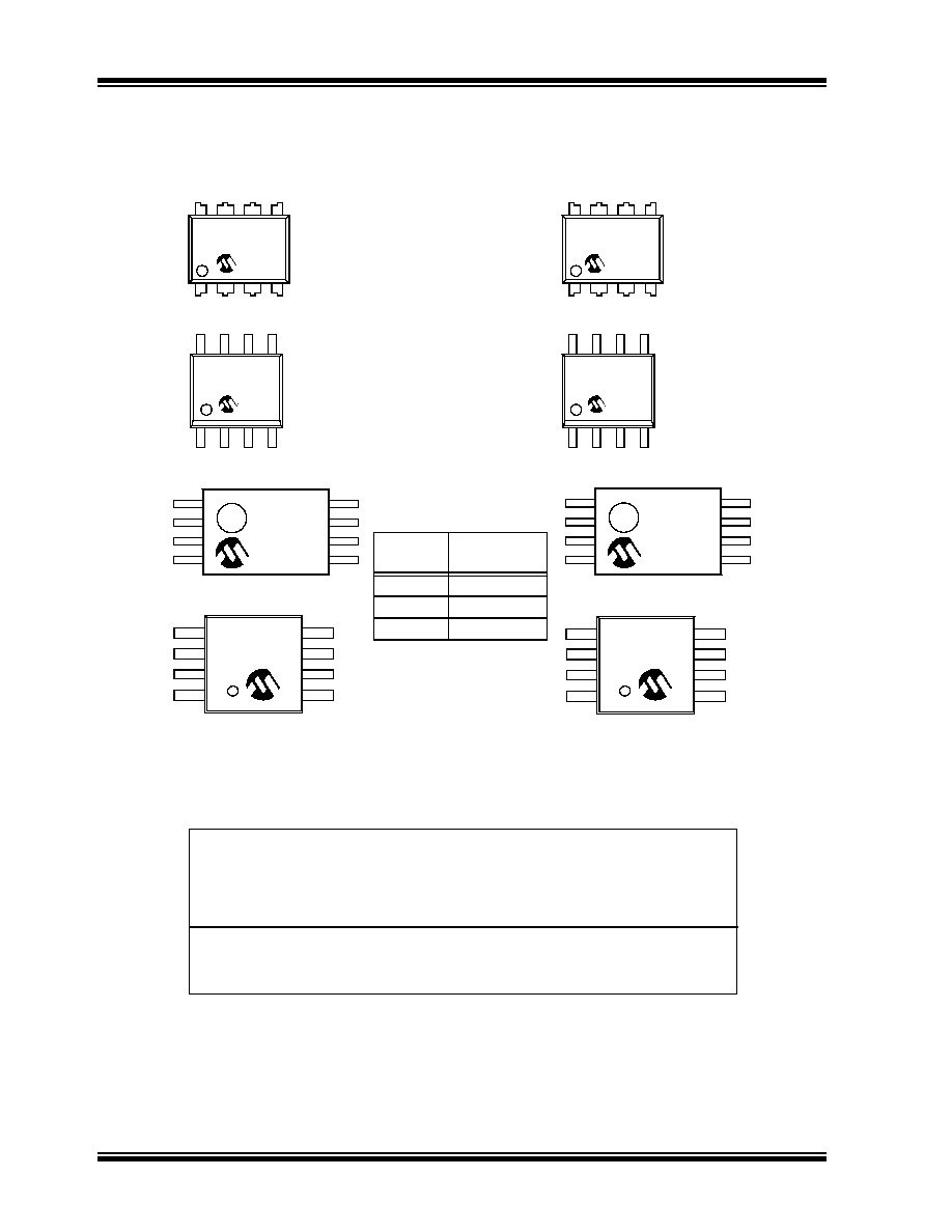
∑ 8-pin PDIP, SOIC, TSSOP and MSOP packages
∑ Available for extended temperature ranges
- Industrial (I): -40∞C to +85∞C
DESCRIPTION
The Microchip Technology Inc. 24AA024/24LC024/
24LC025 is a 2 Kbit Serial Electrically Erasable PROM
with a voltage range of 1.8V to 5.5V. The device is
organized as a single block of 256 x 8-bit memory with
a 2-wire serial interface. Low current design permits
operation with typical standby and active currents of
only 1
µA and 1 mA, respectively. The device has a
page write capability for up to 16 bytes of data.
Functional address lines allow the connection of up to
eight 24AA024/24LC024/24LC025 devices on the
same bus for up to 16K bits of contiguous EEPROM
memory. The device is available in the standard 8-pin
PDIP, 8-pin SOIC (150 mil), TSSOP and MSOP
packages.
PACKAGE TYPES
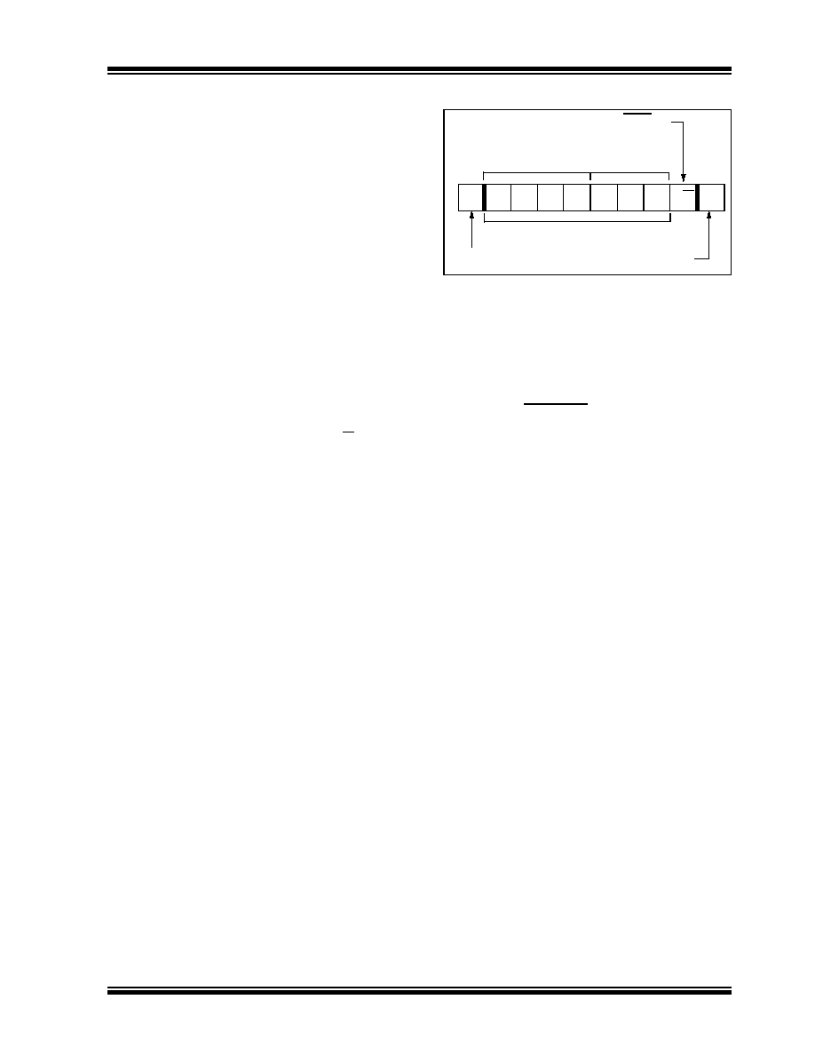
BLOCK DIAGRAM
Part
Number
V
CC
Range
Max
Clock
Temp.
Range
Write
Protect
24AA024 1.8V - 5.5V 400 KHz
(1)
I
Yes
24LC024 2.5V - 5.5V
400 KHz
I
Yes
24LC025
2.5 - 5.5V
400 KHz
I
No
Note 1: 100 KHz for V
CC
< 2.5V
PDIP/SOIC
TSSOP/MSOP
A0
A1
A2
V
SS
V
CC
WP*
SCL
SDA
24AA024
24LC024
24LC025
1
2
3
4
8
7
6
5
A0
A1
A2
V
SS
V
CC
WP*
SCL
SDA
1
2
3
4
8
7
6
5
*WP pin available only on 24XX024. This pin
has no internal connection on 24LC025.
24AA024
24LC024
24LC025
I/O
Control
Logic
Memory
Control
Logic
XDEC
HV Generator
EEPROM
Array
Write Protect
Circuitry
YDEC
V
CC
V
SS
SENSE AMP
R/W CONTROL
SDA SCL
A0 A1 A2
WP*
*WP pin available only on 24XX024. This
pin has no internal connection on 24LC025.
2K I
2
CTM Serial EEPROM
24AA024/24LC024/24LC025
DS21210E-page 2
2003 Microchip Technology Inc.
1.0
ELECTRICAL CHARACTERISTICS
Absolute Maximum Ratings ()
V
CC
.............................................................................................................................................................................6.5V
All inputs and outputs w.r.t. V
SS
......................................................................................................... -0.6V to V
CC
+1.0V
Storage temperature ...............................................................................................................................-65∞C to +150∞C
Ambient temp. with power applied ..........................................................................................................-65∞C to +125∞C
ESD protection on all pins
..................................................................................................................................................... 4 KV
TABLE 1-1:
PIN FUNCTION TABLE
NOTICE: Stresses above those listed under "Absolute Maximum Ratings" may cause permanent damage to the
device. This is a stress rating only and functional operation of the device at those or any other conditions above those
indicated in the operational listings of this specification is not implied. Exposure to maximum rating conditions for
extended periods may affect device reliability.
Name
Function
Vss
SDA
SCL
V
CC
A0, A1, A2
WP
Ground
Serial Data
Serial Clock
1.8V to 5.5V Power Supply
Chip Selects
Hardware Write Protect (24LC024)
TABLE 1-2:
DC CHARACTERISTICS
All parameters apply across the
specified operating ranges unless
otherwise noted.
V
CC
= 1.8V to 5.5V
Industrial (I):
T
AMB
= -40∞C to +85∞C
Parameter
Symbol
Min.
Max.
Units
Conditions
SCL and SDA pins:
High-level input voltage
V
IH
0.7 V
CC
--
V
--
Low-level input voltage
V
IL
0.3 V
CC
V
--
Hysteresis of Schmitt trigger inputs
V
HYS
0.05 V
CC
--
V
(Note)
Low-level output voltage
V
OL
--
0.40
V
I
OL
= 3.0 mA, V
CC
= 4.5V
I
OL
= 2.1 mA, V
CC
= 2.5V
Input leakage current
I
LI
--
±10
µA
V
IN
= 0.1V to 5.5V, WP = V
SS
Output leakage current
I
LO
--
±10
µA
V
OUT
= 0.1V to 5.5V
Pin capacitance (all inputs/outputs)
C
IN
, C
OUT
--
10
pF
V
CC
= 5.0V (Note)
T
AMB
= 25∞C, f = 1 MHz
Operating current
I
CC
Read
--
1
mA
V
CC
= 5.5V, SCL = 400 kHz
I
CC
Write
--
3
mA
V
CC
= 5.5V
Standby current
I
CCS
--
1
µA
V
CC
= 5.5V, SDA = SCL = V
CC
WP = V
SS
, A0, A1, A2 = V
SS
Note:
This parameter is periodically sampled and not 100% tested.
2003 Microchip Technology Inc.
DS21210E-page 3
24AA024/24LC024/24LC025
TABLE 1-3:
AC CHARACTERISTICS
All parameters apply across the specified
operating ranges unless otherwise noted.
V
CC
= 1.8V to 5.5V
Industrial (I):
T
AMB
= -40∞C to +85∞C
Parameter
Symbol
STD MODE
Vcc = 2.5V - 5.5V
FAST MODE
Units
Remarks
Min.
Max.
Min.
Max.
Clock frequency
F
CLK
--
100
--
400
kHz
--
Clock high time
T
HIGH
4000
--
600
--
ns
--
Clock low time
T
LOW
4700
--
1300
--
ns
--
SDA and SCL rise time
T
R
--
1000
--
300
ns
(Note 1)
SDA and SCL fall time
T
F
--
300
--
300
ns
(Note 1)
START condition hold time
T
HD
:
STA
4000
--
600
--
ns
After this period the first
clock pulse is generated
START condition setup time
T
SU
:
STA
4700
--
600
--
ns
Only relevant for repeated
START condition
Data input hold time
T
HD
:
DAT
0
--
0
--
ns
(Note 2)
Data input setup time
T
SU
:
DAT
250
--
100
--
ns
--
STOP condition setup time
T
SU
:
STO
4000
--
600
--
ns
--
Output valid from clock
T
AA
--
3500
--
900
ns
(Note 2)
Bus free time
T
BUF
4700
--
1300
--
ns
Time the bus must be free
before a new transmission
can start
Output fall time from V
IH
minimum to V
IL
maximum
T
OF
--
250
20 +0.1
C
B
250
ns
(Note 1), C
B
100 pF
Input filter spike suppression
(SDA and SCL pins)
T
SP
--
50
--
50
ns
(Note 3)
Write-cycle time
T
WC
--
10
--
10
ms
Byte or Page mode
Endurance
1M
--
1M
--
cycles 25∞C, (Note 4)
Note 1:
Not 100% tested. C
B
= total capacitance of one bus line in pF.
2:
As a transmitter, the device must provide an internal minimum delay time to bridge the undefined region
(minimum 300 ns) of the falling edge of SCL to avoid unintended generation of START or STOP
conditions.
3:
The combined T
SP
and V
HYS
specifications are due to Schmitt Trigger inputs which provide improved
noise spike suppression. This eliminates the need for a TI specification for standard operation.
4:
This parameter is not tested but ensured by characterization. For endurance estimates in a specific
application, please consult the Total EnduranceTM Model which can be downloaded at www.micro-
chip.com.

24AA024/24LC024/24LC025
DS21210E-page 4
2003 Microchip Technology Inc.
FIGURE 1-1:
BUS TIMING DATA
SCL
SDA
IN
T
SU
:
STA
SDA
OUT
T
HD
:
STA
T
LOW
T
HIGH
T
R
T
BUF
T
AA
T
HD
:
DAT
T
SU
:
DAT
T
SU
:
STO
T
SP
T
F

2003 Microchip Technology Inc.
DS21210E-page 5
24AA024/24LC024/24LC025
2.0
PIN DESCRIPTIONS
2.1
SDA Serial Data
SDA is a bi-directional pin used to transfer addresses
and data into and out of the device. It is an open-drain
terminal, therefore the SDA bus requires a pull-up
resistor to V
CC
(typical 10 k
for 100 kHz, 2 k for
400 kHz).
For normal data transfer, SDA is allowed to change
only during SCL low. Changes during SCL high are
reserved for indicating the START and STOP
conditions.
2.2
SCL Serial Clock
The SCL input is used to synchronize the data transfer
from and to the device.
2.3
A0, A1, A2
The levels on the A0, A1 and A2 inputs are compared
with the corresponding bits in the slave address. The
chip is selected if the compare is true.
Up to eight 24AA024/24LC024/24LC025 devices may
be connected to the same bus by using different chip
select bit combinations. These inputs must be
connected to either V
CC
or V
SS
.
2.4
WP (24XX024 only)
WP is the hardware write protect pin. It must be tied to
V
CC
or V
SS
. If tied to Vcc, hardware write protection is
enabled. If WP is tied to Vss, the hardware write protec-
tion is disabled. Note that the WP pin is available only
on the 24XX024. This pin is not internally connected on
the 24LC025.
2.5
Noise Protection
The 24AA024/24LC024/24LC025 employs a V
CC
threshold detector circuit which disables the internal
erase/write logic if the V
CC
is below 1.5 volts at nominal
conditions.
The SCL and SDA inputs have Schmitt Trigger and
filter circuits which suppress noise spikes to assure
proper device operation, even on a noisy bus.
3.0
FUNCTIONAL DESCRIPTION
The 24AA024/24LC024/24LC025 supports a bi-
directional, 2-wire bus and data transmission proto-
col. A device that sends data onto the bus is defined
as transmitter, while a device receiving data is
defined as receiver. The bus has to be controlled by
a master device which generates the serial clock
(SCL), controls the bus access and generates the
START and STOP conditions, while the 24AA024/
24LC024/24LC025 works as slave. Both master and
slave can operate as transmitter or receiver but the
master device determines which mode is activated.
24AA024/24LC024/24LC025
DS21210E-page 6
2003 Microchip Technology Inc.
4.0
BUS CHARACTERISTICS
The following bus protocol has been defined:
∑ Data transfer may be initiated only when the bus
is not busy.
∑ During data transfer, the data line must remain
stable whenever the clock line is HIGH. Changes
in the data line while the clock line is HIGH will be
interpreted as a START or STOP condition.
Accordingly, the following bus conditions have been
defined (Figure 4-1).
4.1
Bus not Busy (A)
Both data and clock lines remain HIGH.
4.2
Start Data Transfer (B)
A HIGH-to-LOW transition of the SDA line while the
clock (SCL) is HIGH determines a START condition. All
commands must be preceded by a START condition.
4.3
Stop Data Transfer (C)
A LOW-to-HIGH transition of the SDA line while the
clock (SCL) is HIGH determines a STOP condition. All
operations must be ended with a STOP condition.
4.4
Data Valid (D)
The state of the data line represents valid data when,
after a START condition, the data line is stable for the
duration of the HIGH period of the clock signal.
The data on the line must be changed during the LOW
period of the clock signal. There is one bit of data per
clock pulse.
Each data transfer is initiated with a START condition
and terminated with a STOP condition. The number of
the data bytes transferred between the START and
STOP conditions is determined by the master device
and is, theoretically, unlimited, (though only the last
sixteen will be stored when performing a write
operation). When an overwrite does occur, it will
replace data in a first-in first-out fashion.
4.5
Acknowledge
Each receiving device, when addressed, is required to
generate an acknowledge after the reception of each
byte. The master device must generate an extra clock
pulse which is associated with this Acknowledge bit.
The device that acknowledges has to pull down the SDA
line during the acknowledge clock pulse in such a way
that the SDA line is stable LOW during the HIGH period
of the acknowledge-related clock pulse. Of course,
setup and hold times must be taken into account. A
master must signal an end of data to the slave by not
generating an Acknowledge bit on the last byte that has
been clocked out of the slave. In this case, the slave
must leave the data line HIGH to enable the master to
generate the STOP condition (Figure 4-2).
FIGURE 4-1:
DATA TRANSFER SEQUENCE ON THE SERIAL BUS CHARACTERISTICS
FIGURE 4-2:
ACKNOWLEDGE TIMING
Note:
The 24AA024/24LC024/24LC025 does
not generate any Acknowledge bits if an
internal programming cycle is in progress.
(A)
(B)
(C)
(D)
(A)
(C)
SCL
SDA
START
CONDITION
ADDRESS OR
ACKNOWLEDGE
VALID
DATA
ALLOWED
TO CHANGE
STOP
CONDITION
SCL
9
8
7
6
5
4
3
2
1
1
2
3
Transmitter must release the SDA line at this point allowing
the Receiver to pull the SDA line low to acknowledge the
previous eight bits of data.
Receiver must release the SDA line at this
point so the Transmitter can continue
sending data.
SDA
Acknowledge
Bit
Data from transmitter
Data from transmitter
2003 Microchip Technology Inc.
DS21210E-page 7
24AA024/24LC024/24LC025
5.0
DEVICE ADDRESSING
A control byte is the first byte received following the
START condition from the master device (Figure 5-1).
The control byte consists of a four-bit control code. For
the 24AA024/24LC024/24LC025, this is set as
1010
binary for read and write operations. The next three bits
of the control byte are the chip select bits (A2, A1, A0).
The chip select bits allow the use of up to eight
24AA024/24LC024/24LC025 devices on the same bus
and are used to select which device is accessed. The
chip select bits in the control byte must correspond to
the logic levels on the corresponding A2, A1 and A0
pins for the device to respond. These bits are in effect
the three most significant bits of the word address.
The last bit of the control byte defines the operation to
be performed. When set to a one, a read operation is
selected. When set to a zero, a write operation is
selected. Following the START condition, the
24AA024/24LC024/24LC025 monitors the SDA bus
checking the control byte being transmitted. Upon
receiving a 1010 code and appropriate chip select bits,
the slave device outputs an Acknowledge signal on the
SDA line. Depending on the state of the R/W bit, the
24AA024/24LC024/24LC025 will select a read or write
operation.
FIGURE 5-1:
CONTROL BYTE FORMAT
5.1
Contiguous Addressing Across
Multiple Devices
The chip select bits A2, A1, A0 can be used to expand
the contiguous address space for up to 16K bits by
adding up to eight 24AA024/24LC024/24LC025
devices on the same bus. In this case, software can
use A0 of the control byte as address bit A8, A1 as
address bit A9 and A2 as address bit A10. It is not
possible to sequentially read across device
boundaries.
1
0
1
0
A2
A1
A0
S
ACK
R/W
Control Code
Chip Select
Bits
Slave Address
Acknowledge Bit
START Bit
Read/Write Bit

24AA024/24LC024/24LC025
DS21210E-page 8
2003 Microchip Technology Inc.
6.0
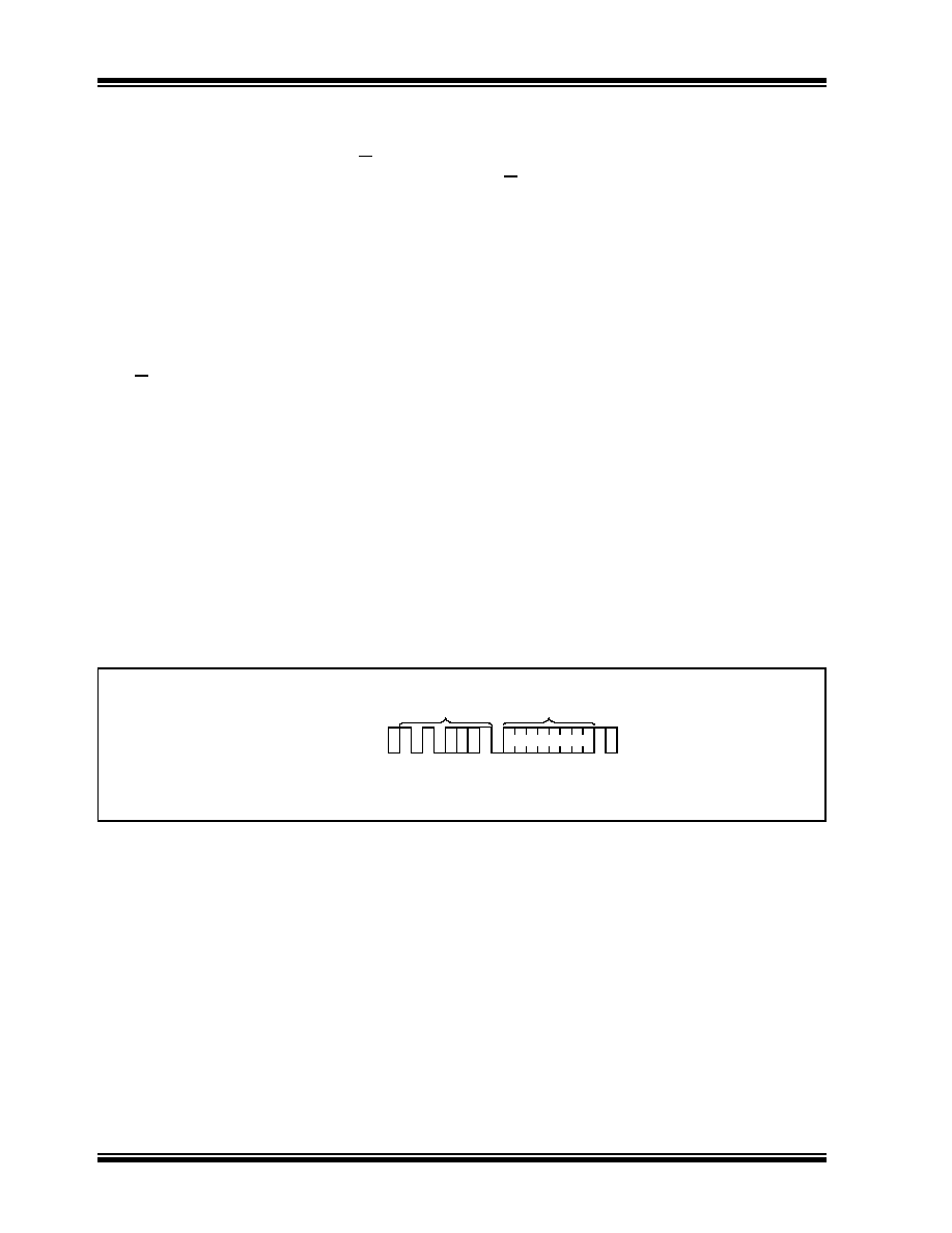
WRITE OPERATIONS
6.1
Byte Write
Following the START signal from the master, the device
code(4 bits), the chip select bits (3 bits) and the R/W bit
(which is a logic-low) is placed onto the bus by the
master transmitter. The device will acknowledge this
control byte during the ninth clock pulse. The next byte
transmitted by the master is the word address and will
be written into the address pointer of the 24AA024/
24LC024/24LC025. After receiving another Acknowl-
edge signal from the 24AA024/24LC024/24LC025, the
master device will transmit the data word to be written
into the addressed memory location. The 24AA024/
24LC024/24LC025 acknowledges again and the
master generates a STOP condition. This initiates the
internal write cycle and, during this time, the 24AA024/
24LC024/24LC025 will not generate Acknowledge
signals (Figure 6-1). If an attempt is made to write to
the protected portion of the array when the hardware
write protection (24XX024 only) has been enabled, the
device will acknowledge the command but no data will
be written. The write cycle time must be observed even
if write protection is enabled.
6.2
Page Write
The write control byte, word address and the first data
byte are transmitted to the 24AA024/24LC024/
24LC025 in the same way as in a byte write. However,
instead of generating a STOP condition, the master
transmits up to 15 additional data bytes to the
24AA024/24LC024/24LC025, which are temporarily
stored in the on-chip page buffer and will be written into
the memory once the master has transmitted a STOP
condition. Upon receipt of each word, the four lower-
order address pointer bits are internally incremented by
one. The higher-order four bits of the word address
remain constant. If the master should transmit more
than 16 bytes prior to generating the STOP condition,
the address counter will roll over and the previously
received data will be overwritten. As with the byte-write
operation, once the STOP condition is received, an
internal write cycle will begin (Figure 6-2). If an attempt
is made to write to the protected portion of the array
when the hardware write-protection has been enabled,
the device will acknowledge the command but no data
will be written. The write cycle time must be observed
even if write protection is enabled.
6.3
WRITE PROTECTION
The WP pin (available on 24XX024 only) must be tied
to V
CC
or V
SS
. If tied to V
CC
, the entire array will be
write-protected. If the WP pin is tied to V
SS
, write
operations to all address locations are allowed.
FIGURE 6-1:
BYTE WRITE
FIGURE 6-2:
PAGE WRITE
Note:
Page write operations are limited to writing
bytes within a single physical page,
regardless of the number of bytes
actually being written. Physical page
boundaries start at addresses that are
integer multiples of the page buffer size (or
`page size') and end at addresses that are
integer multiples of [page size - 1]. If a
page write command attempts to write
across a physical page boundary, the
result is that the data wraps around to the
beginning of the current page (overwriting
data previously stored there), instead of
being written to the next page, as might be
expected. It is therefore necessary for the
application software to prevent page write
operations that would attempt to cross a
page boundary.
S
P
BUS ACTIVITY
MASTER
SDA LINE
BUS ACTIVITY
S
T
A
R
T
S
T
O
P
CONTROL
BYTE
WORD
ADDRESS
DATA
A
C
K
A
C
K
A
C
K
S
P
BUS ACTIVITY
MASTER
SDA LINE
BUS ACTIVITY
S
T
A
R
T
CONTROL
BYTE
WORD
ADDRESS (n)
DATA (n)
DATA (n + 15)
S
T
O
P
A
C
K
A
C
K
A
C
K
A
C
K
A
C
K
DATA (n +1)
2003 Microchip Technology Inc.
DS21210E-page 9
24AA024/24LC024/24LC025
7.0
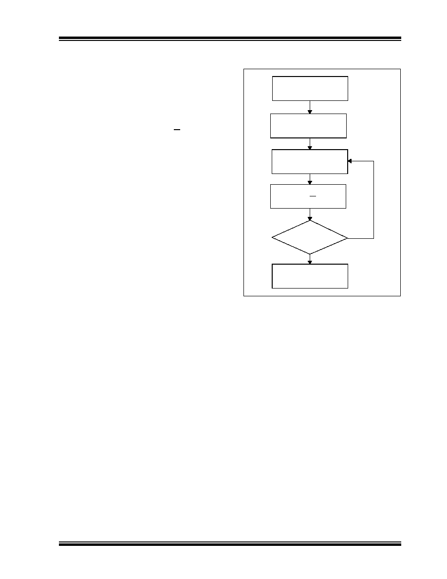
ACKNOWLEDGE POLLING
Since the device will not acknowledge during a write
cycle, this can be used to determine when the cycle is
complete (this feature can be used to maximize bus
throughput). Once the STOP condition for a Write
command has been issued from the master, the device
initiates the internally-timed write cycle, with ACK
polling being initiated immediately. This involves the
master sending a START condition followed by the
control byte for a Write command (R/W = 0). If the
device is still busy with the write cycle, no ACK will be
returned. If no ACK is returned, the START bit and
control byte must be re-sent. If the cycle is complete,
the device will return the ACK and the master can then
proceed with the next Read or Write command. See
Figure 7-1 for a flow diagram of this operation.
FIGURE 7-1:
ACKNOWLEDGE POLLING
FLOW
Send
Write Command
Send STOP
Condition to
Initiate Write Cycle
Send Start
Send Control Byte
with R/W = 0
Did Device
Acknowledge
(ACK = 0)?
Next
Operation
No
Yes
24AA024/24LC024/24LC025
DS21210E-page 10
2003 Microchip Technology Inc.
8.0
READ OPERATIONS
Read operations are initiated in the same way as write
operations, with the exception that the R/W bit of the
slave address is set to `
1
'. There are three basic types
of read operations: current address read, random read
and sequential read.
8.1
Current Address Read
The 24AA024/24LC024/24LC025 contains an address
counter that maintains the address of the last word
accessed, internally incremented by one. Therefore, if
the previous read access was to address n, the next
current address read operation would access data from
address n + 1. Upon receipt of the slave address with
the R/W bit set to `
1
', the 24AA024/24LC024/24LC025
issues an acknowledge and transmits the 8-bit data
word. The master will not acknowledge the transfer but
does generate a STOP condition and the 24AA024/
24LC024/24LC025 discontinues transmission
(Figure 8-1).
8.2
Random Read
Random read operations allow the master to access
any memory location in a random manner. To perform
this type of read operation, the word address must first
be set. This is accomlished by sending the word
address to the 24AA024/24LC024/24LC025 as part of
a write operation. Once the word address is sent, the
master generates a START condition following the
acknowledge. This terminates the write operation, but
not before the internal address pointer is set. The
master then issues the control byte again, but with the
R/W bit set to a `
1
'. The 24AA024/24LC024/24LC025
will then issue an acknowledge and transmits the eight
bit data word. The master will not acknowledge the
transfer but does generate a STOP condition and the
24AA024/24LC024/24LC025 discontinues transmis-
sion (Figure 8-2). After this command, the internal
address counter will point to the address location
following the one that was just read.
8.3
Sequential Read
Sequential reads are initiated in the same way as a
random read except that after the 24AA024/24LC024/
24LC025 transmits the first data byte, the master
issues an acknowledge (as opposed to a STOP
condition in a random read). This directs the 24AA024/
24LC024/24LC025 to transmit the next sequentially-
addressed 8-bit word (Figure 8-3).
To provide sequential reads, the 24AA024/24LC024/
24LC025 contains an internal address pointer that is
incremented by one upon completion of each
operation. This address pointer allows the entire
memory contents to be serially read during one
operation. The internal address pointer will
automatically roll over from address 0FFh to address
000h.
FIGURE 8-1:
CURRENT ADDRESS READ
BUS ACTIVITY
MASTER
SDA LINE
BUS ACTIVITY
P
S
S
T
O
P
CONTROL
BYTE
S
T
A
R
T
DATA
A
C
K
N
O
A
C
K
N
2003 Microchip Technology Inc.
DS21210E-page 11
24AA024/24LC024/24LC025
FIGURE 8-2:
RANDOM READ
FIGURE 8-3:
SEQUENTIAL READ
S
P
S
BUS ACTIVITY
MASTER
SDA LINE
BUS ACTIVITY
S
T
A
R
T
S
T
O
P
CONTROL
BYTE
A
C
K
WORD
ADDRESS (n)
CONTROL
BYTE
S
T
A
R
T
DATA (n)
A
C
K
A
C
K
N
O
A
C
K
BUS ACTIVITY
MASTER
SDA LINE
BUS ACTIVITY
CONTROL
BYTE
DATA (n)
DATA (n + 1)
DATA (n + 2)
DATA (n + X)
N
O
A
C
K
A
C
K
A
C
K
A
C
K
A
C
K
S
T
O
P
P
24AA024/24LC024/24LC025
DS21210E-page 12
2003 Microchip Technology Inc.
9.0
PACKAGING INFORMATION
9.1
Package Marking Information
XXXXXXXX
T/XXXNNN
YYWW
8-Lead PDIP (300 mil)
Example:
8-Lead SOIC (150 mil)
Example:
XXXXXXXX
T/XXYYWW
NNN
8-Lead TSSOP
Example:
24LC024
I/P13F
0319
24LC024
I/SN0319
13F
8-Lead MSOP
Example:
XXXX
TYWW
NNN
XXXXT
YWWNNN
4L24
I319
13F
4L24I
31913F
Legend: XX...X
Customer specific information*
T
Temperature grade
YY
Year code (last 2 digits of calendar year)
WW
Week code (week of January 1 is week `01')
NNN
Alphanumeric traceability code
Note:
In the event the full Microchip part number cannot be marked on one line, it will
be carried over to the next line thus limiting the number of available characters
for customer specific information.
*
Standard OTP marking consists of Microchip part number, year code, week code, and traceability code.
Part
Number
TSSOP/MSOP
Marking Code
24AA024
4A24
24LC024
4L24
24LC025
4L25
2003 Microchip Technology Inc.
DS21210E-page 13
24AA024/24LC024/24LC025
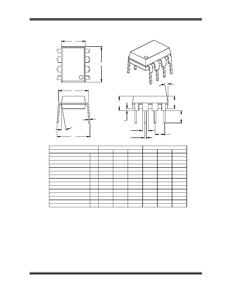
8-Lead Plastic Dual In-line (P) ≠ 300 mil (PDIP)
B1
B
A1
A
L
A2
p
E
eB
c
E1
n
D
1
2
Units
INCHES*
MILLIMETERS
Dimension Limits
MIN
NOM
MAX
MIN
NOM
MAX
Number of Pins
n
8
8
Pitch
p
.100
2.54
Top to Seating Plane
A
.140
.155
.170
3.56
3.94
4.32
Molded Package Thickness
A2
.115
.130
.145
2.92
3.30
3.68
Base to Seating Plane
A1
.015
0.38
Shoulder to Shoulder Width
E
.300
.313
.325
7.62
7.94
8.26
Molded Package Width
E1
.240
.250
.260
6.10
6.35
6.60
Overall Length
D
.360
.373
.385
9.14
9.46
9.78
Tip to Seating Plane
L
.125
.130
.135
3.18
3.30
3.43
Lead Thickness
c
.008
.012
.015
0.20
0.29
0.38
Upper Lead Width
B1
.045
.058
.070
1.14
1.46
1.78
Lower Lead Width
B
.014
.018
.022
0.36
0.46
0.56
Overall Row Spacing
ß
eB
.310
.370
.430
7.87
9.40
10.92
Mold Draft Angle Top
5
10
15
5
10
15
Mold Draft Angle Bottom
5
10
15
5
10
15
* Controlling Parameter
Notes:
Dimensions D and E1 do not include mold flash or protrusions. Mold flash or protrusions shall not exceed
JEDEC Equivalent: MS-001
Drawing No. C04-018
.010" (0.254mm) per side.
ß Significant Characteristic

24AA024/24LC024/24LC025
DS21210E-page 14
2003 Microchip Technology Inc.
8-Lead Plastic Small Outline (SN) ≠ Narrow, 150 mil (SOIC)
Foot Angle
f
0
4
8
0
4
8
15
12
0
15
12
0
Mold Draft Angle Bottom
15
12
0
15
12
0
Mold Draft Angle Top
0.51
0.42
0.33
.020
.017
.013
B
Lead Width
0.25
0.23
0.20
.010
.009
.008
c
Lead Thickness
0.76
0.62
0.48
.030
.025
.019
L
Foot Length
0.51
0.38
0.25
.020
.015
.010
h
Chamfer Distance
5.00
4.90
4.80
.197
.193
.189
D
Overall Length
3.99
3.91
3.71
.157
.154
.146
E1
Molded Package Width
6.20
6.02
5.79
.244
.237
.228
E
Overall Width
0.25
0.18
0.10
.010
.007
.004
A1
Standoff
ß
1.55
1.42
1.32
.061
.056
.052
A2
Molded Package Thickness
1.75
1.55
1.35
.069
.061
.053
A
Overall Height
1.27
.050
p
Pitch
8
8
n
Number of Pins
MAX
NOM
MIN
MAX
NOM
MIN
Dimension Limits
MILLIMETERS
INCHES*
Units
2
1
D
n
p
B
E
E1
h
L
c
45◊
f
A2
A
A1
* Controlling Parameter
Notes:
Dimensions D and E1 do not include mold flash or protrusions. Mold flash or protrusions shall not exceed
.010" (0.254mm) per side.
JEDEC Equivalent: MS-012
Drawing No. C04-057
ß Significant Characteristic
2003 Microchip Technology Inc.
DS21210E-page 15
24AA024/24LC024/24LC025
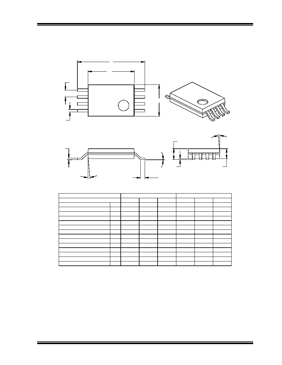
8-Lead Plastic Thin Shrink Small Outline (ST) ≠ 4.4 mm (TSSOP)
10
5
0
10
5
0
Mold Draft Angle Bottom
10
5
0
10
5
0
Mold Draft Angle Top
0.30
0.25
0.19
.012
.010
.007
B
Lead Width
0.20
0.15
0.09
.008
.006
.004
c
Lead Thickness
0.70
0.60
0.50
.028
.024
.020
L
Foot Length
3.10
3.00
2.90
.122
.118
.114
D
Molded Package Length
4.50
4.40
4.30
.177
.173
.169
E1
Molded Package Width
6.50
6.38
6.25
.256
.251
.246
E
Overall Width
0.15
0.10
0.05
.006
.004
.002
A1
Standoff
ß
0.95
0.90
0.85
.037
.035
.033
A2
Molded Package Thickness
1.10
.043
A
Overall Height
0.65
.026
p
Pitch
8
8
n
Number of Pins
MAX
NOM
MIN
MAX
NOM
MIN
Dimension Limits
MILLIMETERS*
INCHES
Units
A2
A
A1
L
c
f
1
2
D
n
p
B
E
E1
Foot Angle
f
0
4
8
0
4
8
* Controlling Parameter
Notes:
Dimensions D and E1 do not include mold flash or protrusions. Mold flash or protrusions shall not exceed
.005" (0.127mm) per side.
JEDEC Equivalent: MO-153
Drawing No. C04-086
ß Significant Characteristic

24AA024/24LC024/24LC025
DS21210E-page 16
2003 Microchip Technology Inc.
8-Lead Plastic Micro Small Outline Package (MSOP)
D
L
c
Dimensions D and E1 do not include mold flash or protrusions. Mold flash or protrusions shall not
.037
.035
F
Footprint (Reference)
exceed.010" (0.254mm) per side.
Notes:
Drawing No. C04-111
*Controlling Parameter
Mold Draft Angle Top
Mold Draft Angle Bottom
Foot Angle
Lead Width
Lead Thickness
c
B
7
7
.004
.010
0
.006
.012
(F)
Dimension Limits
Overall Height
Molded Package Thickness
Molded Package Width
Overall Length
Foot Length
Standoff ß
Overall Width
Number of Pins
Pitch
A
L
E1
D
A1
E
A2
.016
.114
.114
.022
.118
.118
.002
.030
.193
.034
MIN
p
n
Units
.026
NOM
8
INCHES
1.00
0.95
0.90
.039
0.15
0.30
.008
.016
6
0.10
0.25
0
7
7
0.20
0.40
6
MILLIMETERS*
0.65
0.86
3.00
3.00
0.55
4.90
.044
.122
.028
.122
.038
.006
0.40
2.90
2.90
0.05
0.76
MIN
MAX
NOM
1.18
0.70
3.10
3.10
0.15
0.97
MAX
8
E1
E
B
n
1
2
ß Significant Characteristic
.184
.200
4.67
.5.08

2003 Microchip Technology Inc.
DS21210E-page 17
24AA024/24LC024/24LC025
PRODUCT IDENTIFICATION SYSTEM
To order or obtain information, e.g., on pricing or delivery, refer to the factory or the listed sales office
.
Sales and Support
Device:
24AA024: 1.8V, 2 Kbit Addressable Serial EEPROM with
WP pin.
24AA024T:1.8V, 2 Kbit Addressable Serial EEPROM
(Tape and Reel) with WP pin.
24LC024: 2.5V, 2 Kbit Addressable Serial EEPROM with
WP pin.
24LC024T:2.5V, 2 Kbit Addressable Serial EEPROM
(Tape and Reel) with WP pin.
24LC025: 2.5V, 2 Kbit Addressable Serial EEPROM
(Tape and Reel) with no WP pin.
24LC025T:2.5V, 2 Kbit Addressable Serial EEPROM
(Tape and Reel) with no WP pin.
Temperature Range:
I
=
-40∞C to +85∞C
Package:
P
= Plastic DIP, (300 mil Body), 8-lead
SN
= Plastic SOIC, (150 mil Body)
ST
= TSSOP, 8-lead
MS
= MSOP, 8-lead
PART NO.
X
/XX
Package
Temperature
Range
Device
Examples:
a)
24AA024-I/P: Industrial Temperature,
1.8V, PDIP Package
b)
24AA024-I/SN: Industrial Temperature,
1.8V, SOIC Package
c)
24AA024T-I/ST: Industrial Temperature,
1.8V, TSSOP Package, Tape and Reel
d)
24LC024-I/P: Industrial Temperature,
2.5V, PDIP Package
e)
24LC024-I/MS: Industrial Temperature,
2.5V, MSOP Package, Tape and Reel
f)
24LC025-T-I/SN: Industrial Temperature,
2.5V, SOIC Package, Tape and Reel, No
WP
Data Sheets
Products supported by a preliminary Data Sheet may have an errata sheet describing minor operational differences and
recommended workarounds. To determine if an errata sheet exists for a particular device, please contact one of the following:
1.
Your local Microchip sales office
2.
The Microchip Corporate Literature Center U.S. FAX: (480) 792-7277
3.
The Microchip Worldwide Site (www.microchip.com)
Please specify which device, revision of silicon and Data Sheet (include Literature #) you are using.
Customer Notification System
Register on our web site (www.microchip.com/cn) to receive the most current information on our products.

24AA024/24LC024/24LC025
DS21210E-page 18
2003 Microchip Technology Inc.
NOTES:

2003 Microchip Technology Inc.
DS21210E-page 19
Information contained in this publication regarding device
applications and the like is intended through suggestion only
and may be superseded by updates. It is your responsibility to
ensure that your application meets with your specifications.
No representation or warranty is given and no liability is
assumed by Microchip Technology Incorporated with respect
to the accuracy or use of such information, or infringement of
patents or other intellectual property rights arising from such
use or otherwise. Use of Microchip's products as critical
components in life support systems is not authorized except
with express written approval by Microchip. No licenses are
conveyed, implicitly or otherwise, under any intellectual
property rights.
Trademarks
The Microchip name and logo, the Microchip logo, dsPIC,
K
EE
L
OQ
, MPLAB, PIC, PICmicro, PICSTART, PRO MATE and
PowerSmart are registered trademarks of Microchip
Technology Incorporated in the U.S.A. and other countries.
FilterLab, micro
ID, MXDEV, MXLAB, PICMASTER, SEEVAL
and The Embedded Control Solutions Company are
registered trademarks of Microchip Technology Incorporated
in the U.S.A.
Accuron, Application Maestro, dsPICDEM, dsPICDEM.net,
ECONOMONITOR, FanSense, FlexROM, fuzzyLAB, In-
Circuit Serial Programming, ICSP, ICEPIC, microPort,
Migratable Memory, MPASM, MPLIB, MPLINK, MPSIM,
PICC, PICkit, PICDEM, PICDEM.net, PowerCal, PowerInfo,
PowerMate, PowerTool, rfLAB, rfPIC, Select Mode,
SmartSensor, SmartShunt, SmartTel and Total Endurance are
trademarks of Microchip Technology Incorporated in the
U.S.A. and other countries.
Serialized Quick Turn Programming (SQTP) is a service mark
of Microchip Technology Incorporated in the U.S.A.
All other trademarks mentioned herein are property of their
respective companies.
© 2003, Microchip Technology Incorporated, Printed in the
U.S.A., All Rights Reserved.
Printed on recycled paper.
Note the following details of the code protection feature on Microchip devices:
∑
Microchip products meet the specification contained in their particular Microchip Data Sheet.
∑
Microchip believes that its family of products is one of the most secure families of its kind on the market today, when used in the
intended manner and under normal conditions.
∑
There are dishonest and possibly illegal methods used to breach the code protection feature. All of these methods, to our
knowledge, require using the Microchip products in a manner outside the operating specifications contained in Microchip's Data
Sheets. Most likely, the person doing so is engaged in theft of intellectual property.
∑
Microchip is willing to work with the customer who is concerned about the integrity of their code.
∑
Neither Microchip nor any other semiconductor manufacturer can guarantee the security of their code. Code protection does not
mean that we are guaranteeing the product as "unbreakable."
Code protection is constantly evolving. We at Microchip are committed to continuously improving the code protection features of our
products. Attempts to break microchip's code protection feature may be a violation of the Digital Millennium Copyright Act. If such acts
allow unauthorized access to your software or other copyrighted work, you may have a right to sue for relief under that Act.
Microchip received QS-9000 quality system
certification for its worldwide headquarters,
design and wafer fabrication facilities in
Chandler and Tempe, Arizona in July 1999
and Mountain View, California in March 2002.
The Company's quality system processes and
procedures are QS-9000 compliant for its
PICmicro
Æ
8-bit MCUs, K
EE
L
OQ
Æ
code hopping
devices, Serial EEPROMs, microperipherals,
non-volatile memory and analog products. In
addition, Microchip's quality system for the
design and manufacture of development
systems is ISO 9001 certified.

DS21210E-page 20
2003 Microchip Technology Inc.
AMERICAS
Corporate Office
2355 West Chandler Blvd.
Chandler, AZ 85224-6199
Tel: 480-792-7200 Fax: 480-792-7277
Technical Support: 480-792-7627
Web Address: http://www.microchip.com
Atlanta
3780 Mansell Road, Suite 130
Alpharetta, GA 30022
Tel: 770-640-0034 Fax: 770-640-0307
Boston
2 Lan Drive, Suite 120
Westford, MA 01886
Tel: 978-692-3848 Fax: 978-692-3821
Chicago
333 Pierce Road, Suite 180
Itasca, IL 60143
Tel: 630-285-0071 Fax: 630-285-0075
Dallas
4570 Westgrove Drive, Suite 160
Addison, TX 75001
Tel: 972-818-7423 Fax: 972-818-2924
Detroit
Tri-Atria Office Building
32255 Northwestern Highway, Suite 190
Farmington Hills, MI 48334
Tel: 248-538-2250 Fax: 248-538-2260
Kokomo
2767 S. Albright Road
Kokomo, IN 46902
Tel: 765-864-8360 Fax: 765-864-8387
Los Angeles
18201 Von Karman, Suite 1090
Irvine, CA 92612
Tel: 949-263-1888 Fax: 949-263-1338
Phoenix
2355 West Chandler Blvd.
Chandler, AZ 85224-6199
Tel: 480-792-7966 Fax: 480-792-4338
San Jose
Microchip Technology Inc.
2107 North First Street, Suite 590
San Jose, CA 95131
Tel: 408-436-7950 Fax: 408-436-7955
Toronto
6285 Northam Drive, Suite 108
Mississauga, Ontario L4V 1X5, Canada
Tel: 905-673-0699 Fax: 905-673-6509
ASIA/PACIFIC
Australia
Microchip Technology Australia Pty Ltd
Marketing Support Division
Suite 22, 41 Rawson Street
Epping 2121, NSW
Australia
Tel: 61-2-9868-6733 Fax: 61-2-9868-6755
China - Beijing
Microchip Technology Consulting (Shanghai)
Co., Ltd., Beijing Liaison Office
Unit 915
Bei Hai Wan Tai Bldg.
No. 6 Chaoyangmen Beidajie
Beijing, 100027, No. China
Tel: 86-10-85282100 Fax: 86-10-85282104
China - Chengdu
Microchip Technology Consulting (Shanghai)
Co., Ltd., Chengdu Liaison Office
Rm. 2401-2402, 24th Floor,
Ming Xing Financial Tower
No. 88 TIDU Street
Chengdu 610016, China
Tel: 86-28-86766200 Fax: 86-28-86766599
China - Fuzhou
Microchip Technology Consulting (Shanghai)
Co., Ltd., Fuzhou Liaison Office
Unit 28F, World Trade Plaza
No. 71 Wusi Road
Fuzhou 350001, China
Tel: 86-591-7503506 Fax: 86-591-7503521
China - Hong Kong SAR
Microchip Technology Hongkong Ltd.
Unit 901-6, Tower 2, Metroplaza
223 Hing Fong Road
Kwai Fong, N.T., Hong Kong
Tel: 852-2401-1200 Fax: 852-2401-3431
China - Shanghai
Microchip Technology Consulting (Shanghai)
Co., Ltd.
Room 701, Bldg. B
Far East International Plaza
No. 317 Xian Xia Road
Shanghai, 200051
Tel: 86-21-6275-5700 Fax: 86-21-6275-5060
China - Shenzhen
Microchip Technology Consulting (Shanghai)
Co., Ltd., Shenzhen Liaison Office
Rm. 1812, 18/F, Building A, United Plaza
No. 5022 Binhe Road, Futian District
Shenzhen 518033, China
Tel: 86-755-82901380 Fax: 86-755-8295-1393
China - Qingdao
Rm. B505A, Fullhope Plaza,
No. 12 Hong Kong Central Rd.
Qingdao 266071, China
Tel: 86-532-5027355 Fax: 86-532-5027205
India
Microchip Technology Inc.
India Liaison Office
Marketing Support Division
Divyasree Chambers
1 Floor, Wing A (A3/A4)
No. 11, O'Shaugnessey Road
Bangalore, 560 025, India
Tel: 91-80-2290061 Fax: 91-80-2290062
Japan
Microchip Technology Japan K.K.
Benex S-1 6F
3-18-20, Shinyokohama
Kohoku-Ku, Yokohama-shi
Kanagawa, 222-0033, Japan
Tel: 81-45-471- 6166 Fax: 81-45-471-6122
Korea
Microchip Technology Korea
168-1, Youngbo Bldg. 3 Floor
Samsung-Dong, Kangnam-Ku
Seoul, Korea 135-882
Tel: 82-2-554-7200 Fax: 82-2-558-5934
Singapore
Microchip Technology Singapore Pte Ltd.
200 Middle Road
#07-02 Prime Centre
Singapore, 188980
Tel: 65-6334-8870 Fax: 65-6334-8850
Taiwan
Microchip Technology (Barbados) Inc.,
Taiwan Branch
11F-3, No. 207
Tung Hua North Road
Taipei, 105, Taiwan
Tel: 886-2-2717-7175 Fax: 886-2-2545-0139
EUROPE
Austria
Microchip Technology Austria GmbH
Durisolstrasse 2
A-4600 Wels
Austria
Tel: 43-7242-2244-399
Fax: 43-7242-2244-393
Denmark
Microchip Technology Nordic ApS
Regus Business Centre
Lautrup hoj 1-3
Ballerup DK-2750 Denmark
Tel: 45-4420-9895 Fax: 45-4420-9910
France
Microchip Technology SARL
Parc d'Activite du Moulin de Massy
43 Rue du Saule Trapu
Batiment A - ler Etage
91300 Massy, France
Tel: 33-1-69-53-63-20 Fax: 33-1-69-30-90-79
Germany
Microchip Technology GmbH
Steinheilstrasse 10
D-85737 Ismaning, Germany
Tel: 49-89-627-144-0
Fax: 49-89-627-144-44
Italy
Microchip Technology SRL
Via Quasimodo, 12
20025 Legnano (MI)
Milan, Italy
Tel: 39-0331-742611 Fax: 39-0331-466781
United Kingdom
Microchip Ltd.
505 Eskdale Road
Winnersh Triangle
Wokingham
Berkshire, England RG41 5TU
Tel: 44-118-921-5869 Fax: 44-118-921-5820
05/30/03
W
ORLDWIDE
S
ALES
AND
S
ERVICE