 | –≠–ª–µ–∫—Ç—Ä–æ–Ω–Ω—ã–π –∫–æ–º–ø–æ–Ω–µ–Ω—Ç: 24LC32 | –°–∫–∞—á–∞—Ç—å:  PDF PDF  ZIP ZIP |
©
1997 Microchip Technology Inc.
DS21225A-page 1
M
24LC32A MODULE
FEATURES
∑ ISO 7816 compliant contact locations
∑ Single supply with operation down to 2.5V
- Maximum write current 3 mA at 6.0V
- Maximum read current 150
µ
A at 6.0V
- Standby current 1
µ
A max at 2.5V
∑ Two wire serial interface bus, I
2
C
TM
compatible
∑ 100 kHz (2.5V) and 400 kHz (5V) compatibility
∑ Self-timed ERASE and WRITE cycles
∑ Power on/off data protection circuitry
∑ 1,000,000 ERASE/WRITE cycles
guaranteed
∑ 32 byte page or byte write modes available
∑ Schmitt trigger inputs for noise suppression
∑ Output slope control to eliminate ground bounce
∑ 2 ms typical write cycle time, byte or page
∑ Electrostatic discharge protection > 4000V
∑ Data retention > 200 years
∑ 8-pin PDIP and SOIC packages
∑ Temperature ranges:
DESCRIPTION
The Microchip Technology Inc. 24LC32A is a 4K x 8
(32K bit) Serial Electrically Erasable PROM in an ISO
micromodule for use in smart card applications. The
device has a page-write capability of up to 32 bytes.
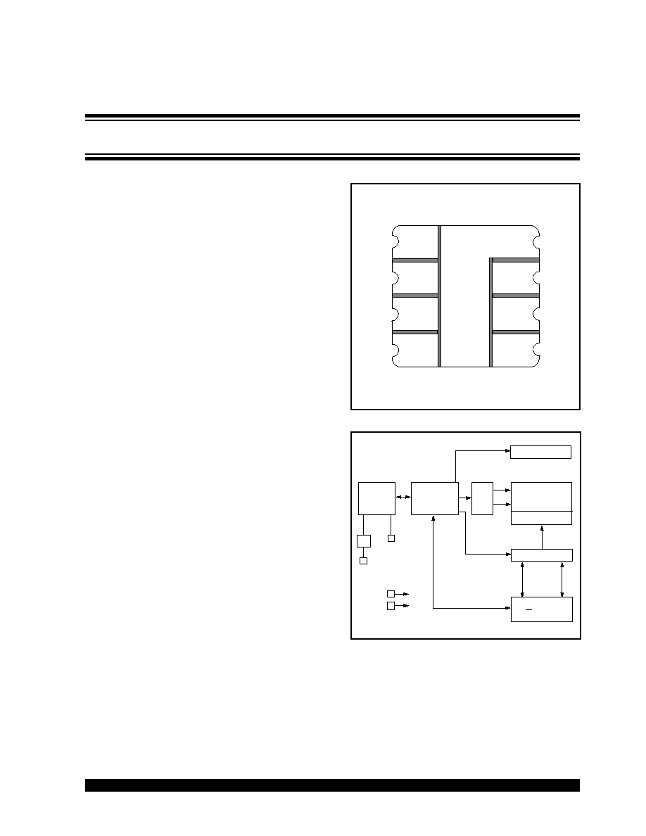
ISO MODULE LAYOUT
BLOCK DIAGRAM
- Commercial:
0∞C
to
+70∞C
V
SS
SDA
SCL
V
DD
HV GENERATOR
EEPROM
ARRAY
PAGE LATCHES
YDEC
XDEC
SENSE AMP
R/W CONTROL
MEMORY
CONTROL
LOGIC
I/O
CONTROL
LOGIC
SDA
SCL
V
CC
V
SS
I/O
32K I
2
CTM Serial EEPROM in ISO Micromodule
I
2
C is a trademark of Philips Corporation.
24LC32A MODULE
DS21225A-page 2
©
1997 Microchip Technology Inc.
1.0
ELECTRICAL CHARACTERISTICS
1.1
Maximum Ratings*
V
CC
........................................................................7.0V
All inputs and outputs w.r.t. V
SS
......-0.6V to V
CC
+1.0V
Storage temperature .......................... -65∞C to +150∞C
Ambient temp. with power applied...... -65∞C to +125∞C
Soldering temperature of leads (10 seconds) .. +300∞C
ESD protection on all pins
.....................................
4 kV
*Notice:
Stresses above those listed under "Maximum Ratings"
may cause permanent damage to the device. This is a stress rat-
ing only and functional operation of the device at those or any
other conditions above those indicated in the operational listings
of this specification is not implied. Exposure to maximum rating
conditions for extended periods may affect device reliability.
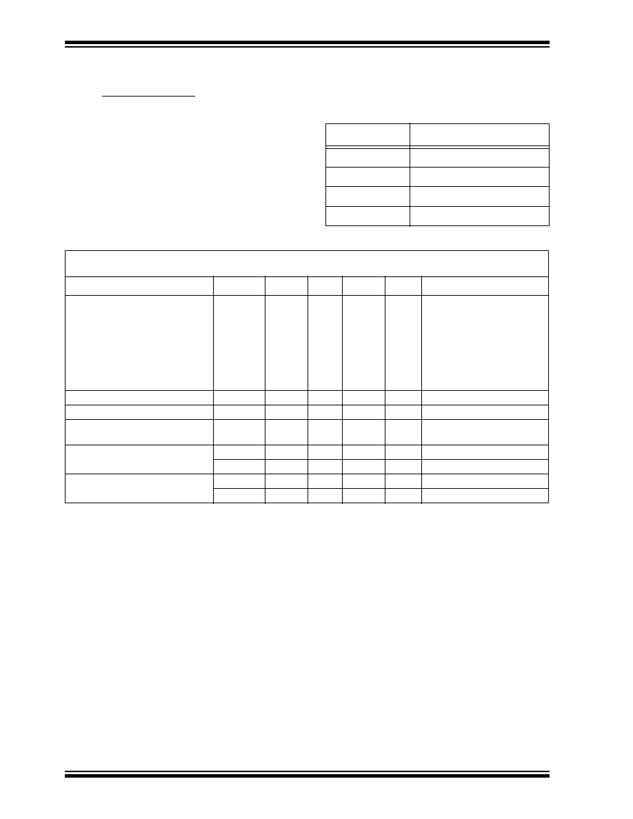
TABLE 1-1:
PIN FUNCTIONS
Name
Function
V
SS
Ground
SDA
Serial Data
SCL
Serial Clock
V
CC
+2.5V to 6.0V Power Supply
TABLE 1-2:
DC CHARACTERISTICS
Vcc = +2.5V to 6.0V
Commercial (C):Tamb = 0∞C to +70
∞
C
Parameter
Symbol
Min
Typ
Max
Units
Conditions
SCL and SDA pins:
High level input voltage
V
IH
.7 V
CC
--
V
Low level input voltage
V
IL
--
.3 Vcc
V
Hysteresis of Schmitt Trigger
inputs
V
HYS
.05 V
CC
--
V
Note 1
Low level output voltage
V
OL
--
.40
V
I
OL
= 3.0 mA @ V
CC
= 4.5V
I
OL
= 2.1 mA @ V
CC
= 2.5V
Input leakage current
I
LI
-10
10
µ
A
V
IN
= .1V to V
CC
Output leakage current
I
LO
-10
10
µ
A
V
OUT
= .1V to V
CC
Pin capacitance
(all inputs/outputs)
C
IN
,C
OUT
--
10
pF
V
CC
= 5.0V (Note 1)
Tamb = 25∞C, f
c
= 1 MHz
Operating current
I
CC
Write
--
3
mA
V
CC
= 6.0V
I
CC
Read
--
400
µ
A
V
CC
= 6.0V, SCL = 400Khz
Standby current
I
CCS
--
1
µ
A
5
µ
A SCL = SDA = V
CC
= 5.0V
I
CCS
1
µ
A
V
CC
= 2.5V (Note 1)
Note 1:
This parameter is periodically sampled and not 100% tested.

24LC32A MODULE
©
1997 Microchip Technology Inc.
DS21225A-page 3
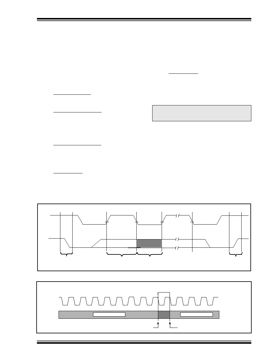
FIGURE 1-1:
BUS TIMING DATA
TABLE 1-3:
AC CHARACTERISTICS
Parameter
Symbol
Vcc = 2.5 - 6.0V
STD. MODE
Vcc = 4.5 - 6.0V
FAST MODE
Units
Remarks
Min
Max
Min
Max
Clock frequency
F
CLK
--
100
--
400
kHz
Clock high time
T
HIGH
4000
--
600
--
ns
Clock low time
T
LOW
4700
--
1300
--
ns
SDA and SCL rise time
T
R
--
1000
--
300
ns
Note 1
SDA and SCL fall time
T
F
--
300
--
300
ns
Note 1
START condition hold
time
T
HD
:
STA
4000
--
600
--
ns
After this period the first clock pulse
is generated
START condition setup
time
T
SU
:
STA
4700
--
600
--
ns
Only relevant for repeated START
condition
Data input hold time
T
HD
:
DAT
0
--
0
--
ns
Data input setup time
T
SU
:
DAT
250
--
100
--
ns
STOP condition setup
time
T
SU
:
STO
4000
--
600
--
ns
Output valid from clock
T
AA
--
3500
--
900
ns
Note 2
Bus free time
T
BUF
4700
--
1300
--
ns
Time the bus must be free before a
new transmission can start
Output fall time from V
IH
min to V
IL
max
T
OF
--
250
20
+0.1C
B
250
ns
Note 1, C
B
100 pF
Input filter spike sup-
pression (SDA and SCL
pins)
T
SP
--
50
--
50
ns
Note 3
Write cycle time
T
WR
--
5
--
5
ms
Byte or Page mode
Note 1:
Not 100% tested. C
B
= total capacitance of one bus line in pF.
2:
As a transmitter, the device must provide an internal minimum delay time to bridge the undefined region
(minimum 300 ns) of the falling edge of SCL to avoid unintended generation of START or STOP conditions.
3:
The combined T
SP
and V
HYS
specifications are due to Schmitt trigger inputs which provide improved noise
and spike suppression. This eliminates the need for a Ti specification for standard operation.
SCL
SDA
IN
T
SU
:
STA
SDA
OUT
T
HD
:
STA
T
LOW
T
HIGH
T
R
T
BUF
T
AA
T
AA
T
HD
:
DAT
T
SU
:
DAT
T
SU
:
STO
T
SP
T
F

24LC32A MODULE
DS21225A-page 4
©
1997 Microchip Technology Inc.
2.0
PIN DESCRIPTIONS
2.1
SDA (Serial Data)
This is a bidirectional pin used to transfer addresses
and data into and data out of the device. It is an open
drain terminal, therefore the SDA bus requires a pullup
resistor to V
CC
(typical 10K
for 100 kHz, 1K
for 400
kHz)
For normal data transfer SDA is allowed to change only
during SCL low. Changes during SCL high are
reserved for indicating the START and STOP condi-
tions.
2.2
SCL (Serial Clock)
This input is used to synchronize the data transfer from
and to the device.
3.0
FUNCTIONAL DESCRIPTION
The 24LC32A supports a bidirectional two-wire bus
and data transmission protocol. A device that sends
data onto the bus is defined as transmitter, and a
device receiving data as receiver. The bus must be con-
trolled by a master device which generates the serial
clock (SCL), controls the bus access, and generates
the START and STOP conditions, while the 24LC32A
works as slave. Both master and slave can operate as
transmitter or receiver but the master device deter-
mines which mode is activated.
24LC32A MODULE
©
1997 Microchip Technology Inc.
DS21225A-page 5
4.0
BUS CHARACTERISTICS
The following bus protocol has been defined:
∑ Data transfer may be initiated only when the bus
is not busy.
∑ During data transfer, the data line must remain
stable whenever the clock line is HIGH. Changes
in the data line while the clock line is HIGH will be
interpreted as a START or STOP condition.
Accordingly, the following bus conditions have been
defined (See Figure 4-1).
4.1
Bus not Busy (A)
Both data and clock lines remain HIGH.
4.2
Start Data Transfer (B)
A HIGH to LOW transition of the SDA line while the
clock (SCL) is HIGH determines a START condition.
All commands must be preceded by a START condi-
tion.
4.3
Stop Data Transfer (C)
A LOW to HIGH transition of the SDA line while the
clock (SCL) is HIGH determines a STOP condition. All
operations must be ended with a STOP condition.
4.4
Data Valid (D)
The state of the data line represents valid data when,
after a START condition, the data line is stable for the
duration of the HIGH period of the clock signal.
The data on the line must be changed during the LOW
period of the clock signal. There is one clock pulse per
bit of data.
Each data transfer is initiated with a START condition
and terminated with a STOP condition. The number of
the data bytes transferred between the START and
STOP conditions is determined by the master device.
4.5
Acknowledge
Each receiving device, when addressed, is obliged to
generate an acknowledge signal after the reception of
each byte. The master device must generate an extra
clock pulse which is associated with this acknowledge
bit.
A device that acknowledges must pull down the SDA
line during the acknowledge clock pulse in such a way
that the SDA line is stable LOW during the HIGH period
of the acknowledge related clock pulse. Of course,
setup and hold times must be taken into account. Dur-
ing reads, a master must signal an end of data to the
slave by NOT generating an acknowledge bit on the
last byte that has been clocked out of the slave. In this
case, the slave (24LC32A) will leave the data line HIGH
to enable the master to generate the STOP condition.
(See Figure 4-2)
FIGURE 4-1:
DATA TRANSFER SEQUENCE ON THE SERIAL BUS
FIGURE 4-2:
ACKNOWLEDGE TIMING
Note:
The 24LC32A does not generate any
acknowledge bits if an internal program-
ming cycle is in progress.
SCL
SDA
START
CONDITION
DATA OR
ACKNOWLEDGE
VALID
DATA
ALLOWED
TO CHANGE
STOP
CONDITION
(A)
(B)
(D)
(D)
(C)
(A)
SCL
9
8
7
6
5
4
3
2
1
1
2
3
Transmitter must release the SDA line at this point allowing the Receiver
to pull the SDA line low to acknowledge the previous eight bits of data.
Receiver must release the SDA line at this point
so the Transmitter can continue sending data.
Data from transmitter
Data from transmitter
SDA
Acknowledge
Bit

24LC32A MODULE
DS21225A-page 6
©
1997 Microchip Technology Inc.
5.0
DEVICE ADDRESSING
A control byte is the first byte received following the
start condition from the master device. (See Figure 5-
1) The control byte consists of a four bit control code;
for the 24LC32A this is set as 1010 binary for read and
write operations. The next three bits are device select
bits on standard devices, however, for micromodules,
these must be zeros. The last bit of the control byte
defines the operation to be performed. When set to a
one a read operation is selected, and when set to a
zero a write operation is selected. The next two bytes
received define the address of the first data byte (see
Figure 5-2). Because only A11...A0 are used, the
upper four address bits must be zeros. The most signif-
icant bit of the most significant byte of the address is
transferred first.
Following the start condition, the 24LC32A monitors
the SDA bus checking the device type identifier being
transmitted. Upon receiving a valid control byte, the
slave device outputs an acknowledge signal on the
SDA line. Depending on the state of the R/W bit, the
24LC32A will select a read or write operation
FIGURE 5-1:
CONTROL BYTE FORMAT
FIGURE 5-2:
ADDRESS SEQUENCE BIT ASSIGNMENTS
1
0
1
0
0
0
0
S
ACK
R/W
Control Code
Device Select
Bits
Slave Address
Acknowledge Bit
Start Bit
Read/Write Bit
ADDRESS BYTE 1
CONTROL BYTE
Slave
Address
Device
Select
Bus
ADDRESS BYTE 0
1
0
1
0
R/W
0
0
0
0
A
11
A
10
A
9
A
7
A
0
A
8
∑
∑
∑
∑
∑
∑
0
0
0
24LC32A MODULE
©
1997 Microchip Technology Inc.
DS21225A-page 7
6.0
WRITE OPERATIONS
6.1
Byte Write
Following the start condition from the master, the con-
trol code (four bits), the device select (three bits), and
the R/W bit which is a logic low are clocked onto the bus
by the master transmitter. This indicates to the
addressed slave receiver that a byte with a word
address will follow after it has generated an acknowl-
edge bit during the ninth clock cycle. Therefore the next
byte transmitted by the master is the high-order byte of
the word address and will be written into the address
pointer of the 24LC32A MODULE. The next byte is the
least significant address byte. After receiving another
acknowledge signal from the 24LC32A the master
device will transmit the data word to be written into the
addressed memory location.
The 24LC32A acknowledges again and the master
generates a stop condition. This initiates the internal
write cycle, and during this time the 24LC32A will not
generate acknowledge signals (see Figure 6-1).
6.2
Page Write
The write control byte, word address and the first data
byte are transmitted to the 24LC32A in the same way
as in a byte write. But instead of generating a stop con-
dition, the master transmits up to 32 bytes which are
temporarily stored in the on-chip page buffer and will be
written into memory after the master has transmitted a
stop condition. After receipt of each word, the five lower
address pointer bits are internally incremented by one.
If the master should transmit more than 32 bytes prior
to generating the stop condition, the address counter
will roll over and the previously received data will be
overwritten. As with the byte write operation, once the
stop condition is received, an internal write cycle will
begin. (see Figure 6-2).
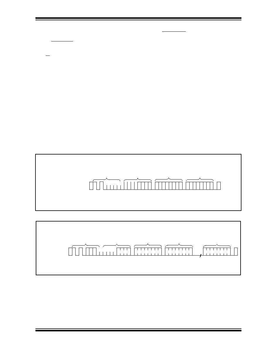
FIGURE 6-1:
BYTE WRITE
FIGURE 6-2:
PAGE WRITE
S
T
A
R
T
S
T
O
P
ADDRESS
HIGH BYTE
DATA
CONTROL
BYTE
A
C
K
A
C
K
A
C
K
BUS ACTIVITY
MASTER
SDA LINE
BUS ACTIVITY
A
C
K
ADDRESS
LOW BYTE
0 0 0 0
0 0 0 0
0
0
1
1
S
T
A
R
T
S
T
O
P
ADDRESS
HIGH BYTE
CONTROL
BYTE
A
C
K
A
C
K
A
C
K
BUS ACTIVITY
MASTER
SDA LINE
BUS ACTIVITY
A
C
K
ADDRESS
LOW BYTE
0 0 0 0
DATA BYTE 0
A
C
K
DATA BYTE 31
0 0 0 0
0
0
1
1
24LC32A MODULE
DS21225A-page 8
©
1997 Microchip Technology Inc.
7.0
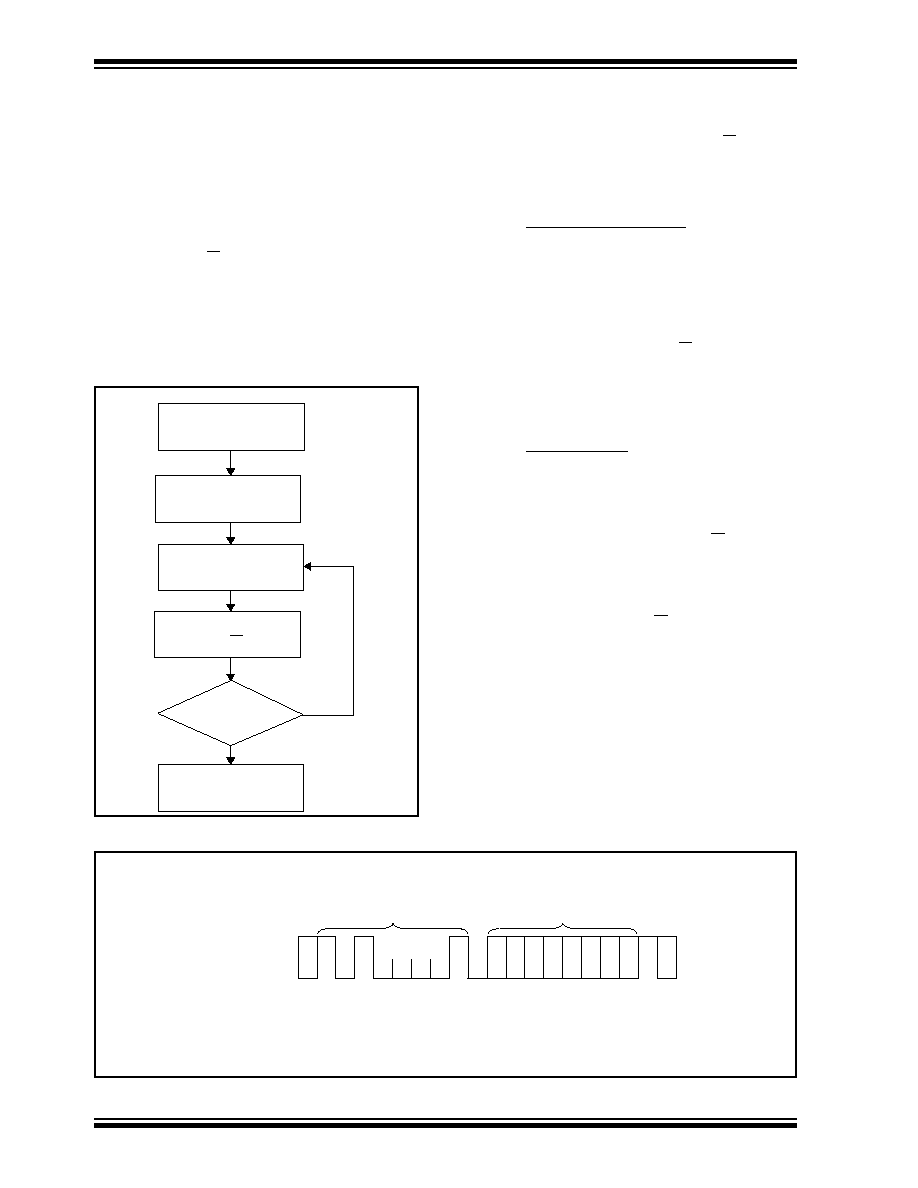
ACKNOWLEDGE POLLING
Since the device will not acknowledge during a write
cycle, this can be used to determine when the cycle is
complete (this feature can be used to maximize bus
throughput). Once the stop condition for a write com-
mand has been issued from the master, the device ini-
tiates the internally timed write cycle. ACK polling can
be initiated immediately. This involves the master send-
ing a start condition followed by the control byte for a
write command (R/W = 0). If the device is still busy with
the write cycle, then no ACK will be returned. If the
cycle is complete, then the device will return the ACK
and the master can then proceed with the next read or
write command. See Figure 7-1 for flow diagram.
FIGURE 7-1:
ACKNOWLEDGE POLLING
FLOW
8.0
READ OPERATION
Read operations are initiated in the same way as write
operations with the exception that the R/W bit of the
slave address is set to one. There are three basic types
of read operations: current address read, random read,
and sequential read.
8.1
Current Address Read
The 24LC32A contains an address counter that main-
tains the address of the last word accessed, internally
incremented by one. Therefore, if the previous access
(either a read or write operation) was to address n (n is
any legal address), the next current address read oper-
ation would access data from address n + 1. Upon
receipt of the slave address with R/W bit set to one, the
24LC32A issues an acknowledge and transmits the
eight bit data word. The master will not acknowledge
the transfer but does generate a stop condition and the
24LC32A discontinues transmission (see Figure 8-1).
8.2
Random Read
Random read operations allow the master to access
any memory location in a random manner. To perform
this type of read operation, first the word address must
be set. This is done by sending the word address to the
24LC32A as part of a write operation (R/W bit set to 0).
After the word address is sent, the master generates a
start condition following the acknowledge. This termi-
nates the write operation, but not before the internal
address pointer is set. Then the master issues the con-
trol byte again but with the R/W bit set to a one. The
24LC32A will then issue an acknowledge and transmit
the eight bit data word. The master will not acknowl-
edge the transfer but does generate a stop condition
which causes the 24LC32A to discontinue transmis-
sion (see Figure 8-2).
FIGURE 8-1:
CURRENT ADDRESS READ
Send
Write Command
Send Stop
Condition to
Initiate Write Cycle
Send Start
Send Control Byte
with R/W = 0
Did Device
Acknowledge
(ACK = 0)?
Next
Operation
NO
YES
S
P
S
T
A
R
T
S
T
O
P
DATA BYTE
CONTROL BYTE
A
C
K
N
O
A
C
K
BUS ACTIVITY
MASTER
SDA LINE
BUS ACTIVITY
0
1
0 0 0
1
1
0

24LC32A MODULE
©
1997 Microchip Technology Inc.
DS21225A-page 9
8.3
Sequential Read
Sequential reads are initiated in the same way as a ran-
dom read except that after the 24LC32A transmits the
first data byte, the master issues an acknowledge as
opposed to the stop condition used in a random read.
This acknowledge directs the 24LC32A to transmit the
next sequentially addressed 8 bit word (see Figure 8-
3). Following the final byte transmitted to the master,
the master will NOT generate an acknowledge but will
generate a stop condition.
To provide sequential reads the 24LC32A contains an
internal address pointer which is incremented by one at
the completion of each operation. This address pointer
allows the entire memory contents to be serially read
during one operation. The internal address pointer will
automatically roll over from address 0FFF to address
000 if the master acknowledges the byte received from
the array address 0FFF.
FIGURE 8-2:
RANDOM READ
FIGURE 8-3:
SEQUENTIAL READ
S
T
A
R
T
S
T
O
P
ADDRESS
HIGH BYTE
CONTROL
BYTE
A
C
K
A
C
K
N
O
A
C
K
BUS ACTIVITY
MASTER
SDA LINE
BUS ACTIVITY
A
C
K
ADDRESS
LOW BYTE
0 0 0 0
CONTROL
BYTE
A
C
K
DATA
BYTE
S
T
A
R
T
0 0 0 0
0
0 1
1
S
0 0 0 1
0
0 1
1
S
S
T
O
P
CONTROL
BYTE
A
C
K
A
C
K
A
C
K
BUS ACTIVITY
MASTER
SDA LINE
BUS ACTIVITY
A
C
K
N
O
A
C
K
DATA n
DATA n +1
DATA n +2
DATA n + X
24LC32A MODULE
DS21225A-page 10
©
1997 Microchip Technology Inc.
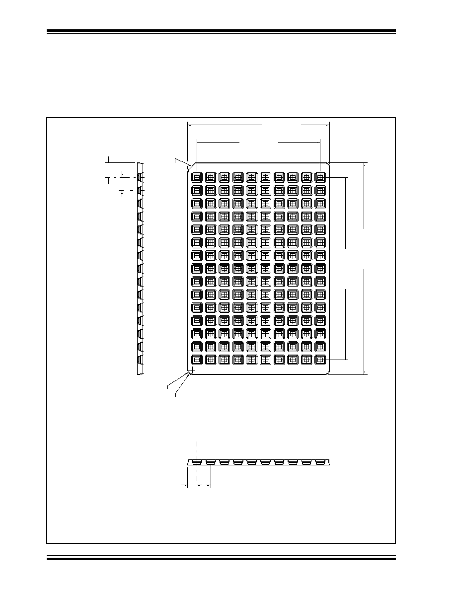
9.0
SHIPPING METHOD
The micromodules will be shipped to customers in
clear plastic trays. Each tray holds 150 modules, and
the trays can be stacked in a manner similar to shipping
die in waffle packs. A tray drawing with dimensions is
shown in Figure 9-1.
FIGURE 9-1:
TRAY DIMENSIONS
SMART CARD MODULES
14.000 [355.60]
12.040 [305.82]
9.374 [238.09]
0.500 [12.70]
0.980 [24.89] TYP
0.860 [21.84] TYP.
0.617 [15.68]
0.905 [22.99]
R 0.300 [7.62] TYP
R 0.270 [6.86] TYP
8.145 [206.88]
ANTISTATIC

24LC32A MODULE
©
1997 Microchip Technology Inc.
DS21225A-page 11
FIGURE 9-2:
MODULE DIMENSIONS
0.465
±
0.002
[11.80
±
0.05]
0.419
±
0.002
[10.63
±
0.05]
A
A
0.270 [6.86] MAX.
0.232
±
0.002
[5.90
±
0.05]
R. 0.059 [1.50] (4X)
0.090 [2.29] MIN EPOXY
FREE AREA (TYP.)
0.1043
±
0.002
[2.65
±
0.05]
(8x)
0.146
±
0.002
[3.71
±
0.05]
0.174
±
0.002
[4.42
±
0.05]
0.209
±
0.002
[5.31
±
0.05]
TYP.
DEVICE SIDE
CONTACT SIDE
0.1043
±
0.002
[2.65
±
0.05]
0.285 [7.24] MAX
VIA HOLES (8x)
I.D. Ø 0.026 [0.66]
O.D. Ø 0.042 [1.06]
GOLD FLASH 3-7
0.004 [0.10] MAX.
COPPER BASE NICKEL PLATED, 150 MIN
GLOB SIZE
0.007 [0.18] MAX.
SECTION A-A
FR4 TAPE
DIE
m
IN
m
IN
0.015 [0.38] MAX.
0.0235 [0.60] MAX.

24LC32A MODULE
DS21225A-page 12
©
1997 Microchip Technology Inc.
NOTES:

24LC32A MODULE
©
1997 Microchip Technology Inc.
DS21225A-page 13
NOTES:

24LC32A MODULE
DS21225A-page 14
©
1997 Microchip Technology Inc.
NOTES:

24LC32A MODULE
©
1997 Microchip Technology Inc.
DS21225A-page 15
24LC32A MODULE PRODUCT IDENTIFICATION SYSTEM
To order or obtain information, e.g., on pricing or delivery, refer to the factory or the listed sales office.
Sales and Support
Package:
MT = Micromodules in trays
Temperature
Range:
Blank = 0∞C to +70∞C
Device:
24LC32A
32K bit 2.5V I
2
C Serial EEPROM in ISO Module
24LC32A
--
/MT
Data Sheets
Products supported by a preliminary Data Sheet may have an errata sheet describing minor operational differences and recom-
mended workarounds. To determine if an errata sheet exists for a particular device, please contact one of the following:
1.
Your local Microchip sales office.
2.
The Microchip Corporate Literature Center U.S. FAX: (602) 786-7277.
3.
The Microchip's Bulletin Board, via your local CompuServe number (CompuServe membership NOT required).
Please specify which device, revision of silicon and Data Sheet (include Literature #) you are using.

Information contained in this publication regarding device applications and the like is intended for suggestion only and may be superseded by updates. No representation or
warranty is given and no liability is assumed by Microchip Technology Incorporated with respect to the accuracy or use of such information, or infringement of patents or other
intellectual property rights arising from such use or otherwise. Use of Microchip's products as critical components in life support systems is not authorized except with express
written approval by Microchip. No licenses are conveyed, implicitly or otherwise, under any intellectual property rights. The Microchip logo and name are registered trademarks
of Microchip Technology Inc. in the U.S.A. and other countries. All rights reserved. All other trademarks mentioned herein are the property of their respective companies.
DS21225A-page 16
©
1997 Microchip Technology Inc.
M
All rights reserved. © 1997, Microchip Technology Incorporated, USA. 9/97
Printed on recycled paper.
AMERICAS
Corporate Office
Microchip Technology Inc.
2355 West Chandler Blvd.
Chandler, AZ 85224-6199
Tel: 602-786-7200 Fax: 602-786-7277
Technical Support:
602 786-7627
Web:
http://www.microchip.com
Atlanta
Microchip Technology Inc.
500 Sugar Mill Road, Suite 200B
Atlanta, GA 30350
Tel: 770-640-0034 Fax: 770-640-0307
Boston
Microchip Technology Inc.
5 Mount Royal Avenue
Marlborough, MA 01752
Tel: 508-480-9990 Fax: 508-480-8575
Chicago
Microchip Technology Inc.
333 Pierce Road, Suite 180
Itasca, IL 60143
Tel: 630-285-0071 Fax: 630-285-0075
Dallas
Microchip Technology Inc.
14651 Dallas Parkway, Suite 816
Dallas, TX 75240-8809
Tel: 972-991-7177 Fax: 972-991-8588
Dayton
Microchip Technology Inc.
Two Prestige Place, Suite 150
Miamisburg, OH 45342
Tel: 937-291-1654 Fax: 937-291-9175
Los Angeles
Microchip Technology Inc.
18201 Von Karman, Suite 1090
Irvine, CA 92612
Tel: 714-263-1888 Fax: 714-263-1338
New York
Microchip Technology Inc.
150 Motor Parkway, Suite 416
Hauppauge, NY 11788
Tel: 516-273-5305 Fax: 516-273-5335
San Jose
Microchip Technology Inc.
2107 North First Street, Suite 590
San Jose, CA 95131
Tel: 408-436-7950 Fax: 408-436-7955
Toronto
Microchip Technology Inc.
5925 Airport Road, Suite 200
Mississauga, Ontario L4V 1W1, Canada
Tel: 905-405-6279 Fax: 905-405-6253
ASIA/PACIFIC
Hong Kong
Microchip Asia Pacific
RM 3801B, Tower Two
Metroplaza
223 Hing Fong Road
Kwai Fong, N.T., Hong Kong
Tel: 852-2-401-1200 Fax: 852-2-401-3431
India
Microchip Technology Inc.
India Liaison Office
No. 6, Legacy, Convent Road
Bangalore 560 025, India
Tel: 91-80-229-4036 Fax: 91-80-559-9840
Korea
Microchip Technology Korea
168-1, Youngbo Bldg. 3 Floor
Samsung-Dong, Kangnam-Ku
Seoul, Korea
Tel: 82-2-554-7200 Fax: 82-2-558-5934
Shanghai
Microchip Technology
RM 406 Shanghai Golden Bridge Bldg.
2077 Yan'an Road West, Hong Qiao District
Shanghai, PRC 200335
Tel: 86-21-6275-5700
Fax: 86 21-6275-5060
Singapore
Microchip Technology Taiwan
Singapore Branch
200 Middle Road
#07-02 Prime Centre
Singapore 188980
Tel: 65-334-8870 Fax: 65-334-8850
Taiwan, R.O.C
Microchip Technology Taiwan
10F-1C 207
Tung Hua North Road
Taipei, Taiwan, ROC
Tel: 886 2-717-7175 Fax: 886-2-545-0139
EUROPE
United Kingdom
Arizona Microchip Technology Ltd.
Unit 6, The Courtyard
Meadow Bank, Furlong Road
Bourne End, Buckinghamshire SL8 5AJ
Tel: 44-1628-851077 Fax: 44-1628-850259
France
Arizona Microchip Technology SARL
Zone Industrielle de la Bonde
2 Rue du Buisson aux Fraises
91300 Massy, France
Tel: 33-1-69-53-63-20 Fax: 33-1-69-30-90-79
Germany
Arizona Microchip Technology GmbH
Gustav-Heinemann-Ring 125
D-81739 M¸chen, Germany
Tel: 49-89-627-144 0 Fax: 49-89-627-144-44
Italy
Arizona Microchip Technology SRL
Centro Direzionale Colleoni
Palazzo Taurus 1 V. Le Colleoni 1
20041 Agrate Brianza
Milan, Italy
Tel: 39-39-6899939 Fax: 39-39-6899883
JAPAN
Microchip Technology Intl. Inc.
Benex S-1 6F
3-18-20, Shinyokohama
Kohoku-Ku, Yokohama-shi
Kanagawa 222 Japan
Tel: 81-45-471- 6166 Fax: 81-45-471-6122
8/29/97
W
ORLDWIDE
S
ALES
& S
ERVICE