 | –≠–ª–µ–∫—Ç—Ä–æ–Ω–Ω—ã–π –∫–æ–º–ø–æ–Ω–µ–Ω—Ç: 24LCS21T | –°–∫–∞—á–∞—Ç—å:  PDF PDF  ZIP ZIP |

©
1999 Microchip Technology Inc.
DS21127D-page 1
FEATURES
∑ Completely implements DDC1
TM
/DDC2
TM
interface for monitor identification
∑ Hardware write-protect pin
∑ Single supply with operation down to 2.5V
∑ Low power CMOS technology
- 1 mA active current typical
- 10
µ
A standby current typical at 5.5V
∑ 2-wire serial interface bus, I
2
C
TM
compatible
(SCL)
∑ Self-timed write cycle (including auto-erase)
∑ Page-write buffer for up to 8 bytes
∑ 100 kHz (2.5V) and 400 kHz (5V) compatibility
(SCL)
∑ 1,000,000 erase/write cycles guaranteed
∑ Data retention > 200 years
∑ 8-pin PDIP and SOIC package
∑ Available for extended temperature ranges
DESCRIPTION
The Microchip Technology Inc. 24LCS21 is a
128 x 8-bit dual-mode Electrically Erasable PROM.
This device is designed for use in applications requiring
storage and serial transmission of configuration and
control information. Two modes of operation have been
implemented: Transmit Only Mode and bi-directional
Mode. Upon power-up, the device will be in the
Transmit Only Mode, sending a serial bit stream of the
entire memory array contents, clocked by the VCLK
pin. A valid high to low transition on the SCL pin will
cause the device to enter the bi-directional Mode, with
byte selectable read/write capability of the memory
array in standard I
2
C protocol.
The 24LCS21 also enables the user to write-protect the
entire memory contents using its write-protect pin. The
24LCS21 is available in a standard 8-pin PDIP and
SOIC package in both commercial and industrial
temperature ranges.
- Commercial
(C):
0∞C to +70∞C
- Industrial (I)
-40∞C to +85∞C
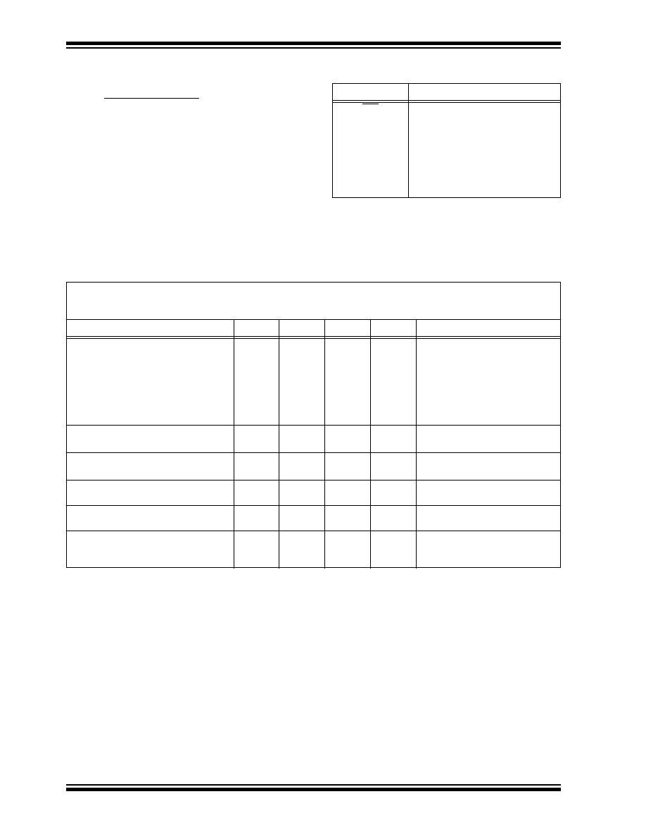
PACKAGE TYPES
BLOCK DIAGRAM
24LCS21
SOIC
1
2
3
4
8
7
6
5
V
CC
VCLK
SCL
SDA
NC
NC
WP
V
SS
24LCS21
PDIP
1
2
3
4
8
7
6
5
V
CC
VCLK
SCL
SDA
NC
NC
WP
V
SS
I/O
CONTROL
LOGIC
EEPROM
ARRAY
PAGE LATCHES
HV GENERATOR
SENSE AMP
R/W CONTROL
MEMORY
CONTROL
LOGIC
XDEC
YDEC
V
CC
V
SS
SDA SCL
VCLK
WP
24LCS21
1K 2.5V Dual Mode I
2
C
TM
Serial EEPROM
DDC is a trademark of the Video Electronics Standards Association.
I
2
C is a trademark of Philips Corporation.
24LCS21
DS21127D-page 2
©
1999 Microchip Technology Inc.
1.0
ELECTRICAL CHARACTERISTICS
1.1
Maximum Ratings*
V
CC
...................................................................................7.0V
All inputs and outputs w.r.t. V
SS
................-0.6V to V
CC
+1.0V
Storage temperature .....................................-65
∞
C to +150
∞
C
Ambient temp. with power applied.................-65
∞
C to +125
∞
C
Soldering temperature of leads (10 seconds) ............. +300
∞
C
ESD protection on all pins
..................................................
4 kV
*Notice:
Stresses above those listed under "Maximum ratings"
may cause permanent damage to the device. This is a stress rat-
ing only and functional operation of the device at those or any
other conditions above those indicated in the operational listings
of this specification is not implied. Exposure to maximum rating
conditions for extended periods may affect device reliability.
TABLE 1-1:
PIN FUNCTION TABLE
Name
Function
WP
Write Protect (active low)
V
SS
Ground
SDA
Serial Address/Data I/O
SCL
Serial Clock (Bi-directional Mode)
VCLK
Serial Clock (Transmit-Only Mode)
V
CC
+2.5V to 5.5V Power Supply
NC
No Connection
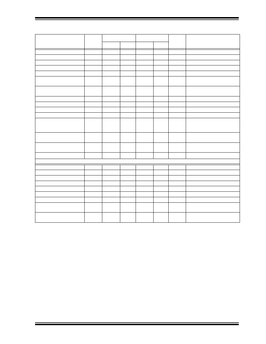
TABLE 1-2:
DC CHARACTERISTICS
V
CC
= +2.5V to 5.5V
Commercial
(C):
Tamb = 0
∞
C to +70
∞
C
Industrial (I):
Tamb
= -40
∞
C to +85
∞
C
Parameter
Symbol
Min
Max
Units
Conditions
SCL and SDA pins:
High level input voltage
Low level input voltage
V
IH
V
IL
0.7 V
CC
0.3 V
CC
V
V
Input levels on VCLK pin:
High level input voltage
Low level input voltage
V
IH
V
IL
2.0
0.8
0.2 V
CC
V
V
V
CC
2.7V (Note)
V
CC
< 2.7V (Note)
Hysteresis of Schmitt trigger inputs
V
HYS
.05 V
CC
--
V
(Note)
Low level output voltage
V
OL1
0.4
V
I
OL
= 3 mA, V
CC
= 2.5V (Note 1)
Low level output voltage
V
OL2
0.6
V
I
OL
= 6 mA, V
CC
= 2.5V
Input leakage current
I
LI
-10
10
µ
A
V
IN
= 0.1V to V
CC
Output leakage current
I
LO
-10
10
µ
A
V
OUT
= 0.1V to V
CC
Pin capacitance (all inputs/outputs)
C
INT
10
pF
V
CC
= 5.0V (Note1),
Tamb = 25
∞
C, F
CLK
= 1 MHz
Operating current
I
CC
Write
I
CC
Read
--
--
3
1
mA
mA
V
CC
= 5.5V, SCL = 400 kHz
Standby current
I
CCS
--
30
100
µ
A
µ
A
V
CC
= 3.0V, SDA = SCL = V
CC
V
CC
= 5.5V, SDA = SCL = V
CC
V
CLK
= V
SS
Note: This parameter is periodically sampled and not 100% tested.
©
1999 Microchip Technology Inc.
DS21127D-page 3
24LCS21
TABLE 1-3:
AC CHARACTERISTICS
Parameter
Symbol
Vcc= 2.5-5.5V
Vcc= 4.5 - 5.5V
Units
Remarks
Min
Max
Min
Max
Clock frequency
F
CLK
0
100
0
400
kHz
Clock high time
T
HIGH
4000
--
600
--
ns
Clock low time
T
LOW
4700
--
1300
--
ns
SDA and SCL rise time
T
R
--
1000
--
300
ns
(Note 1)
SDA and SCL fall time
T
F
--
300
--
300
ns
(Note 1)
START condition hold time
T
HD
:
STA
4000
--
600
--
ns
After this period the first clock
pulse is generated
START condition setup time
T
SU
:
STA
4700
--
600
--
ns
Only relevant for repeated
START condition
Data input hold time
T
HD
:
DAT
0
--
0
--
ns
(Note 2)
Data input setup time
T
SU
:
DAT
250
--
100
--
ns
STOP condition setup time
T
SU
:
STO
4000
--
600
--
ns
Output valid from clock
T
AA
--
3500
--
900
ns
(Note 2)
Bus free time
T
BUF
4700
--
1300
--
ns
Time the bus must be free
before a new transmission can
start
Output fall time from V
IH
minimum to V
IL
maximum
T
OF
--
250
20 + 0.1
C
B
250
ns
(Note 1), C
B
100 pF
Input filter spike suppression
(SDA and SCL pins)
T
SP
--
100
--
50
ns
(Note 3)
Write cycle time
T
WR
--
10
--
10
ms
Byte or Page mode
Transmit-Only Mode Parameters
Output valid from VCLK
T
VAA
--
2000
--
1000
ns
VCLK high time
T
VHIGH
4000
--
600
--
ns
VCLK low time
T
VLOW
4700
--
1300
--
ns
VCLK setup time
T
VHST
0
--
0
--
ns
VCLK hold time
T
SPVL
4000
--
600
--
ns
Mode transition time
T
VHZ
--
500
--
500
ns
Transmit-Only power up time
T
VPU
0
--
0
--
ns
Input filter spike suppression
(VCLK pin)
T
SPV
--
100
--
100
ns
Endurance
--
1M
--
1M
--
cycles
25∞C, V
CC
= 5.0V, Block Mode
(Note 4)
Note 1: Not 100% tested. C
B
= total capacitance of one bus line in pF.
2: As a transmitter, the device must provide an internal minimum delay time to bridge the undefined region
(minimum 300 ns) of the falling edge of SCL to avoid unintended generation of START or STOP conditions.
3: The combined T
SP
and V
HYS
specifications are due to Schmitt trigger inputs which provide noise and spike
suppression. This eliminates the need for a T
I
specification for standard operation.
4: This parameter is not tested but guaranteed by characterization. For endurance estimates in a specific appli-
cation, please consult the Total Endurance Model which can be obtained on our website.
24LCS21
DS21127D-page 4
©
1999 Microchip Technology Inc.
2.0
FUNCTIONAL DESCRIPTION
The 24LCS21 operates in two modes, the
Transmit-Only Mode and the bi-directional Mode. There
is a separate two wire protocol to support each mode,
each having a separate clock input but sharing a com-
mon data line (SDA). The device enters the Trans-
mit-Only Mode upon power-up. In this mode, the device
transmits data bits on the SDA pin in response to a
clock signal on the VCLK pin. The device will remain in
this mode until a valid high to low transition is placed on
the SCL input. When a valid transition on SCL is recog-
nized, the device will switch into the bi-directional
Mode. The only way to switch the device back to the
Transmit-Only Mode is to remove power from the
device.
2.1
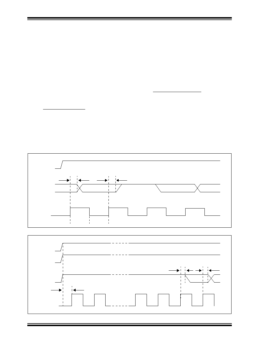
Transmit-Only Mode
The device will power up in the Transmit-Only Mode at
address 00H. This mode supports a unidirectional two
wire protocol for continuous transmission of the
contents of the memory array. This device requires that
it be initialized prior to valid data being sent in the
Transmit-Only Mode (see Initialization Procedure,
below). In this mode, data is transmitted on the SDA
pin in 8-bit bytes, with each byte followed by a ninth, null
bit (Figure 2-1). The clock source for the Transmit-Only
Mode is provided on the VCLK pin, and a data bit is out-
put on the rising edge on this pin. The eight bits in each
byte are transmitted most significant bit first. Each byte
within the memory array will be output in sequence.
When the last byte in the memory array is transmitted,
the internal address pointers will wrap around to the
first memory location (00H) and continue. The bi-direc-
tional Mode Clock (SCL) pin must be held high for the
device to remain in the Transmit-Only Mode.
2.2
Initialization Procedure
After V
CC
has stabilized, the device will be in the
Transmit-Only Mode. Nine clock cycles on the VCLK
pin must be given to the device for it to perform internal
sychronization. During this period, the SDA pin will be
in a high impedance state. On the rising edge of the
tenth clock cycle, the device will output the first valid
data bit which will be the most significant bit in address
00h. (Figure 2-2).
FIGURE 2-1: TRANSMIT ONLY MODE
FIGURE 2-2: DEVICE INITIALIZATION
SCL
SDA
VCLK
T
VAA
T
VAA
Bit 1 (LSB)
Null Bit
Bit 1 (MSB)
Bit 7
T
VLOW
T
VHIGH
T
VAA
T
VAA
Bit 8
Bit 7
High Impedance for 9 clock cycles
T
VPU
1
2
8
9
10
11
SCL
SDA
VCLK
Vcc
©
1999 Microchip Technology Inc.
DS21127D-page 5
24LCS21
3.0
BI-DIRECTIONAL MODE
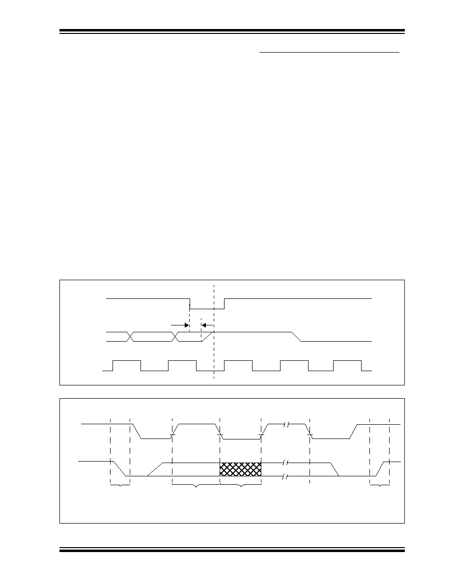
The 24LCS21 can be switched into the bi-directional
Mode (Figure 3-1) by applying a valid high to low
transition on the bi-directional Mode Clock (SCL).
When the device has been switched into the bi-direc-
tional Mode, the VCLK input is disregarded, with the
exception that a logic high level is required to enable
write capability. This mode supports a two-wire
bi-directional data transmission protocol (I
2
C
TM
). In this
protocol, a device that sends data on the bus is defined
to be the transmitter, and a device that receives data
from the bus is defined to be the receiver. The bus must
be controlled by a master device that generates the
bi-directional Mode Clock (SCL), controls access to the
bus and generates the START and STOP conditions,
while the 24LCS21 acts as the slave. Both master and
slave can operate as transmitter or receiver, but the
master device determines which mode is activated.
In this mode, the 24LCS21 only responds to
commands for device 1010 000X.
3.1 Bi-directional Mode Bus Characteristics
The following bus protocol has been defined:
∑ Data transfer may be initiated only when the bus
is not busy.
∑ During data transfer, the data line must remain
stable whenever the clock line is HIGH. Changes
in the data line while the clock line is HIGH will be
interpreted as a START or STOP condition.
Accordingly, the following bus conditions have been
defined (Figure 3-2).
3.1.1
BUS NOT BUSY (A)
Both data and clock lines remain HIGH.
3.1.2
START DATA TRANSFER (B)
A HIGH to LOW transition of the SDA line while the
clock (SCL) is HIGH determines a START condition. All
commands must be preceded by a START condition.
3.1.3
STOP DATA TRANSFER (C)
A LOW to HIGH transition of the SDA line while the
clock (SCL) is HIGH determines a STOP condition. All
operations must be ended with a STOP condition.
FIGURE 3-1: MODE TRANSITION
FIGURE 3-2: DATA TRANSFER SEQUENCE ON THE SERIAL BUS
SCL
SDA
VCLK
Bi-directional Mode
T
VHZ
Transmit Only Mode
(A)
(B)
(D)
(D)
(A)
(C)
START
CONDITION
ADDRESS OR
ACKNOWLEDGE
VALID
DATA
ALLOWED
TO CHANGE
STOP
CONDITION
SCL
SDA
24LCS21
DS21127D-page 6
©
1999 Microchip Technology Inc.
3.1.4
DATA VALID (D)
The state of the data line represents valid data when,
after a START condition, the data line is stable for the
duration of the HIGH period of the clock signal.
The data on the line must be changed during the LOW
period of the clock signal. There is one clock pulse per
bit of data.
Each data transfer is initiated with a START condition
and terminated with a STOP condition. The number of
the data bytes transferred between the START and
STOP conditions is determined by the master device
and is theoretically unlimited, although only the last
eight will be stored when doing a write operation. When
an overwrite does occur it will replace data in a first in
first out fashion.
3.1.5
ACKNOWLEDGE
Each receiving device, when addressed, is obliged to
generate an acknowledge after the reception of each
byte. The master device must generate an extra clock
pulse which is associated with this acknowledge bit.
The device that acknowledges has to pull down the
SDA line during the acknowledge clock pulse in such a
way that the SDA line is stable LOW during the HIGH
period of the acknowledge related clock pulse. Of
course, setup and hold times must be taken into
account. A master must signal an end of data to the
slave by not generating an acknowledge bit on the last
byte that has been clocked out of the slave. In this
case, the slave must leave the data line HIGH to enable
the master to generate the STOP condition.
Note:
Once switched into bi-directional Mode,
the 24LCS21 will remain in that mode until
power goes away. Removing power is the
only way to reset the 24LCS21 into the
Transmit-only mode.
Note:
The 24LCS21 does not generate any
acknowledge bits if an internal
programming cycle is in progress.
FIGURE 3-3: BUS TIMING START/STOP
FIGURE 3-4: BUS TIMING DATA
T
SU
:
STA
T
HD
:
STA
V
HYS
T
SU
:
STO
START
STOP
SCL
SDA
SCL
SDA
IN
SDA
OUT
T
SU
:
STA
T
SP
T
AA
T
F
T
LOW
T
HIGH
T
HD
:
STA
T
HD
:
DAT
T
SU
:
DAT
T
SU
:
STO
T
BUF
T
AA
T
R

©
1999 Microchip Technology Inc.
DS21127D-page 7
24LCS21
3.1.6
SLAVE ADDRESS
After generating a START condition, the bus master
transmits the slave address consisting of a 7-bit device
code (1010000) for the 24LCS21.
The eighth bit of slave address determines whether the
master device wants to read or write to the 24LCS21
(Figure 3-5).
The 24LCS21 monitors the bus for its corresponding
slave address continuously. It generates an
acknowledge bit if the slave address was true and it is
not in a programming mode.
FIGURE 3-5: CONTROL BYTE ALLOCATION
4.0
WRITE OPERATION
4.1
Byte Write
Following the start signal from the master, the slave
address (4 bits), three zero bits (000) and the R/W bit
which is a logic low are placed onto the bus by the
master transmitter. This indicates to the addressed
slave receiver that a byte with a word address will follow
after it has generated an acknowledge bit during the
ninth clock cycle. Therefore, the next byte transmitted
by the master is the word address and will be written
into the address pointer of the 24LCS21. After receiv-
ing another acknowledge signal from the 24LCS21 the
master device will transmit the data word to be written
into the addressed memory location. The 24LCS21
acknowledges again and the master generates a stop
condition. This initiates the internal write cycle, and dur-
ing this time the 24LCS21 will not generate acknowl-
edge signals (Figure 4-1).
It is required that VCLK be held at a logic high level
during command and data transfer in order to program
the device. This applies to both byte write and page
write operation. Note, however, that the VCLK is
ignored during the self-timed program operation.
Changing VCLK from high to low during the self-timed
program operation will not halt programming of the
device.
Operation
Slave Address
R/W
Read
1010000
1
Write
1010000
0
SLAVE ADDRESS
1
0
1
0
0
0
0
R/W
A
START
READ/WRITE
FIGURE 4-1: BYTE WRITE
FIGURE 4-2: VCLK WRITE ENABLE TIMING
BUS ACTIVITY:
MASTER
SDA LINE
BUS ACTIVITY:
CONTROL
BYTE
WORD
ADDRESS
DATA
S
T
O
P
S
T
A
R
T
A
C
K
S
P
A
C
K
A
C
K
VCLK
T
SPVL
T
SU
:
STO
T
HD
:
STA
T
VHST
VCLK
SDA
IN
SCL
24LCS21
DS21127D-page 8
©
1999 Microchip Technology Inc.
4.2
Page Write
The write control byte, word address and the first data
byte are transmitted to the 24LCS21 in the same way
as in a byte write. But instead of generating a stop
condition the master transmits up to eight data bytes to
the 24LCS21 which are temporarily stored in the
on-chip page buffer and will be written into the memory
after the master has transmitted a stop condition. After
the receipt of each word, the three lower order address
pointer bits are internally incremented by one. The
higher order five bits of the word address remains
constant. If the master should transmit more than eight
words prior to generating the stop condition, the
address counter will roll over and the previously
received data will be overwritten. As with the byte write
operation, once the stop condition is received an
internal write cycle will begin (Figure 5-2).
It is required that VCLK be held at a logic high level
during command and data transfer in order to program
the device. This applies to both byte write and page
write operation. Note, however, that the VCLK is
ignored during the self-timed program operation.
Changing VCLK from high to low during the self-timed
program operation will not halt programming of the
device.
5.0
ACKNOWLEDGE POLLING
Since the device will not acknowledge during a write
cycle, this can be used to determine when the cycle is
complete (this feature can be used to maximize bus
throughput). Once the stop condition for a write
command has been issued from the master, the device
initiates the internally timed write cycle. ACK polling
can be initiated immediately. This involves the master
sending a start condition followed by the control byte for
a write command (R/W = 0). If the device is still busy
with the write cycle, then no ACK will be returned. If the
cycle is complete, then the device will return the ACK
and the master can then proceed with the next read or
write command. See Figure 5-1 for the flow diagram.
FIGURE 5-1: ACKNOWLEDGE POLLING FLOW
Note:
Page write operations are limited to writing
bytes within a single physical page, regard-
less of the number of bytes actually being
written. Physical page boundaries start at
addresses that are integer multiples of the
page buffer size (or ‘page size’) and end at
addresses that are integer multiples of
[page size - 1]. If a page write command
attempts to write across a physical page
boundary, the result is that the data wraps
around to the beginning of the current page
(overwriting data previously stored there),
instead of being written to the next page as
might be expected. It is therefore neces-
sary for the application software to prevent
page write operations that would attempt to
cross a page boundary.
Did Device
Acknowledge
(ACK = 0)?
Send
Write Command
Send Stop
Condition to
Initiate Write Cycle
Send Start
Send Control Byte
with R/W = 0
Next
Operation
No
Yes
FIGURE 5-2: PAGE WRITE
BUS
MASTER
SDA LINE
BUS
CONTROL
BYTE
WORD
ADDRESS
S
T
O
P
S
T
A
R
T
A
C
K
A
C
K
A
C
K
ACTIVITY:
ACTIVITY:
A
C
K
A
C
K
DATA n + 1
DATA n + 7
DATA (n)
P
S
VCLK

©
1999 Microchip Technology Inc.
DS21127D-page 9
24LCS21
6.0
WRITE PROTECTION
When using the 24LCS21 in the bi-directional Mode,
the VCLK pin operates as the write protect control pin.
Setting VCLK high allows normal write operations,
while setting VCLK low prevents writing to any location
in the array. Connecting the VCLK pin to V
SS
would
allow the 24LCS21 to operate as a serial ROM,
although this configuration would prevent using the
device in the Transmit-Only Mode.
Additionally, Pin 3 performs a flexible write protect
function. The 24LCS21 contains a write-protection
control fuse whose factory default state is cleared.
Writing any data to address 7Fh (normally the
checksum in DDC applications) sets the fuse which
enables the WP pin. Until this fuse is set, the 24LCS21
is always write enabled (if VCLK = 1). After the fuse is
set, the write capability of the 24LCS21 is determined
by WP (Figure 6-1).
FIGURE 6-1: WRITE PROTECT TRUTH
TABLE
7.0
READ OPERATION
Read operations are initiated in the same way as write
operations with the exception that the R/W bit of the
slave address is set to one. There are three basic types
of read operations: current address read, random read
and sequential read.
7.1
Current Address Read
The 24LCS21 contains an address counter that
maintains the address of the last word accessed,
internally incremented by one. Therefore, if the
previous access (either a read or write operation) was
to address n, the next current address read operation
would access data from address n + 1. Upon receipt of
the slave address with R/W bit set to one, the 24LCS21
issues an acknowledge and transmits the eight bit data
word. The master will not acknowledge the transfer but
does generate a stop condition and the 24LCS21
discontinues transmission (Figure 7-1).
FIGURE 7-1: CURRENT ADDRESS READ
7.2
Random Read
Random read operations allow the master to access
any memory location in a random manner. To perform
this type of read operation, first the word address must
be set. This is done by sending the word address to the
24LCS21 as part of a write operation. After the word
address is sent, the master generates a start condition
following the acknowledge. This terminates the write
operation, but not before the internal address pointer is
set. Then the master issues the control byte again but
with the R/W bit set to a one. The 24LCS21 will then
issue an acknowledge and transmits the eight bit data
word. The master will not acknowledge the transfer but
does generate a stop condition and the 24LCS21
discontinues transmission (Figure 7-2).
VCLK
WP
Add. 7Fh
Written
Mode
0
X
X
Read Only
1
X
No
R/W
1
1/open
Yes
R/W
1
0
Yes
Read Only
CONTROL
A
C
K
S
S
T
A
R
T
S
T
O
P
P
BYTE
DATA n
BUS ACTIVITY
SDA LINE
BUS ACTIVITY
A
C
K
N
O
MASTER
1 0 1 0 0 0 0 1
FIGURE 7-2: RANDOM READ
BUS ACTIVITY
MASTER
SDA LINE
BUS ACTIVITY
CONTROL
BYTE
WORD
ADDRESS
DATA n
A
C
K
S
T
A
R
T
N
O
S
T
A
R
CONTROL
BYTE
A
C
K
A
C
K
A
C
K
S
S
T
P
S
T
O
P
1 0 1 0 0 0 0 0
0
0
0
0
0
1
1
1

24LCS21
DS21127D-page 10
©
1999 Microchip Technology Inc.
7.3
Sequential Read
Sequential reads are initiated in the same way as a
random read except that after the 24LCS21 transmits
the first data byte, the master issues an acknowledge
as opposed to a stop condition in a random read. This
directs the 24LCS21 to transmit the next sequentially
addressed 8-bit word (Figure 8-1).
To provide sequential reads the 24LCS21 contains an
internal address pointer which is incremented by one at
the completion of each operation. This address pointer
allows the entire memory contents to be serially read
during one operation.
7.4
Noise Protection
The 24LCS21 employs a V
CC
threshold detector circuit
which disables the internal erase/write logic if the V
CC
is below 1.5 volts at nominal conditions.
The SDA, SCL and VCLK inputs have Schmitt trigger
and filter circuits which suppress noise spikes to assure
proper device operation even on a noisy bus.
8.0
PIN DESCRIPTIONS
8.1
SDA
This pin is used to transfer addresses and data into and
out of the device, when the device is in the bi-direc-
tional Mode. In the Transmit-Only Mode, which only
allows data to be read from the device, data is also
transferred on the SDA pin. This pin is an open drain
terminal, therefore the SDA bus requires a pullup
resistor to V
CC
(typical 10 K
for 100 kHz, 2 K
for
400 kHz).
For normal data transfer in the bi-directional Mode,
SDA is allowed to change only during SCL low.
Changes during SCL high are reserved for indicating
the START and STOP conditions.
8.2
SCL
This pin is the clock input for the bi-directional Mode,
and is used to synchronize data transfer to and from the
device. It is also used as the signaling input to switch
the device from the Transmit Only Mode to the bi-direc-
tional Mode. It must remain high for the chip to continue
operation in the Transmit Only Mode.
8.3
VCLK
This pin is the clock input for the Transmit Only Mode
(DDC1). In the Transmit Only Mode, each bit is clocked
out on the rising edge of this signal. In the bi-directional
Mode, a high logic level is required on this pin to enable
write capability.
8.4
WP
This pin is used for flexible write protection of the
24LCS21. When the last memory location (7Fh) is
written with any data, this pin is enabled and
determines the write capability of the 24LCS21
(Figure 6-1).
The WP pin has an internal pull up resistor which will
allow write capability (assuming VCLK = 1) at all times
if this pin is floated.
FIGURE 8-1: SEQUENTIAL READ
A
C
K
P
BUS ACTIVITY
MASTER
SDA LINE
BUS ACTIVITY
CONTROL
BYTE
DATA n
DATA n+1
DATA n+2
DATA n+X
A
C
K
A
C
K
A
C
K
N
O
A
C
K
S
T
O
P
24LCS21
©
1999 Microchip Technology Inc.
DS21127D-page 11
24LCS21 Product Identification System
To order or to obtain information (e.g., on pricing or delivery), please use the listed part numbers, and refer to the factory or the listed
sales offices.
Sales and Support
Data Sheets
Products supported by a preliminary Data Sheet may have an errata sheet describing minor operational differences and recommended
workarounds. To determine if an errata sheet exists for a particular device, please contact one of the following:
1.
Your local Microchip sales office
2.
The Microchip Corporate Literature Center U.S. FAX: (602) 786-7277
3.
The Microchip Worldwide Site (www.microchip.com)
Please specify which device, revision of silicon and Data Sheet (include Literature #) you are using.
New Customer Notification System
Register on our web site (www.microchip.com/cn) to receive the most current information on our products.
Package:
P = Plastic DIP (300 mil Body), 8-lead
SN = Plastic SOIC (150 mil Body), 8-lead
Temperature
Blank = 0∞C to +70∞C
Range:
I
= -40∞C to +85∞C
Device:
24LCS21
Dual Mode I
2
C Serial EEPROM
24LCS21T
Dual Mode I
2
C Serial EEPROM (Tape and Reel)
24LCS21
≠
/P
2002 Microchip Technology Inc.
Information contained in this publication regarding device
applications and the like is intended through suggestion only
and may be superseded by updates. It is your responsibility to
ensure that your application meets with your specifications.
No representation or warranty is given and no liability is
assumed by Microchip Technology Incorporated with respect
to the accuracy or use of such information, or infringement of
patents or other intellectual property rights arising from such
use or otherwise. Use of Microchip's products as critical com-
ponents in life support systems is not authorized except with
express written approval by Microchip. No licenses are con-
veyed, implicitly or otherwise, under any intellectual property
rights.
Trademarks
The Microchip name and logo, the Microchip logo, FilterLab,
K
EE
L
OQ
, microID, MPLAB, PIC, PICmicro, PICMASTER,
PICSTART, PRO MATE, SEEVAL and The Embedded Control
Solutions Company are registered trademarks of Microchip Tech-
nology Incorporated in the U.S.A. and other countries.
dsPIC, ECONOMONITOR, FanSense, FlexROM, fuzzyLAB,
In-Circuit Serial Programming, ICSP, ICEPIC, microPort,
Migratable Memory, MPASM, MPLIB, MPLINK, MPSIM,
MXDEV, PICC, PICDEM, PICDEM.net, rfPIC, Select Mode
and Total Endurance are trademarks of Microchip Technology
Incorporated in the U.S.A.
Serialized Quick Turn Programming (SQTP) is a service mark
of Microchip Technology Incorporated in the U.S.A.
All other trademarks mentioned herein are property of their
respective companies.
© 2002, Microchip Technology Incorporated, Printed in the
U.S.A., All Rights Reserved.
Printed on recycled paper.
Microchip received QS-9000 quality system
certification for its worldwide headquarters,
design and wafer fabrication facilities in
Chandler and Tempe, Arizona in July 1999. The
Company's quality system processes and
procedures are QS-9000 compliant for its
PICmicro
Æ
8-bit MCUs, K
EE
L
OQ
Æ
code hopping
devices, Serial EEPROMs and microperipheral
products. In addition, Microchip's quality
system for the design and manufacture of
development systems is ISO 9001 certified.
Note the following details of the code protection feature on PICmicro
Æ
MCUs.
∑
The PICmicro family meets the specifications contained in the Microchip Data Sheet.
∑
Microchip believes that its family of PICmicro microcontrollers is one of the most secure products of its kind on the market today,
when used in the intended manner and under normal conditions.
∑
There are dishonest and possibly illegal methods used to breach the code protection feature. All of these methods, to our knowl-
edge, require using the PICmicro microcontroller in a manner outside the operating specifications contained in the data sheet.
The person doing so may be engaged in theft of intellectual property.
∑
Microchip is willing to work with the customer who is concerned about the integrity of their code.
∑
Neither Microchip nor any other semiconductor manufacturer can guarantee the security of their code. Code protection does not
mean that we are guaranteeing the product as "unbreakable".
∑
Code protection is constantly evolving. We at Microchip are committed to continuously improving the code protection features of
our product.
If you have any further questions about this matter, please contact the local sales office nearest to you.

2002 Microchip Technology Inc.
M
AMERICAS
Corporate Office
2355 West Chandler Blvd.
Chandler, AZ 85224-6199
Tel: 480-792-7200 Fax: 480-792-7277
Technical Support: 480-792-7627
Web Address: http://www.microchip.com
Rocky Mountain
2355 West Chandler Blvd.
Chandler, AZ 85224-6199
Tel: 480-792-7966 Fax: 480-792-7456
Atlanta
500 Sugar Mill Road, Suite 200B
Atlanta, GA 30350
Tel: 770-640-0034 Fax: 770-640-0307
Boston
2 Lan Drive, Suite 120
Westford, MA 01886
Tel: 978-692-3848 Fax: 978-692-3821
Chicago
333 Pierce Road, Suite 180
Itasca, IL 60143
Tel: 630-285-0071 Fax: 630-285-0075
Dallas
4570 Westgrove Drive, Suite 160
Addison, TX 75001
Tel: 972-818-7423 Fax: 972-818-2924
Detroit
Tri-Atria Office Building
32255 Northwestern Highway, Suite 190
Farmington Hills, MI 48334
Tel: 248-538-2250 Fax: 248-538-2260
Kokomo
2767 S. Albright Road
Kokomo, Indiana 46902
Tel: 765-864-8360 Fax: 765-864-8387
Los Angeles
18201 Von Karman, Suite 1090
Irvine, CA 92612
Tel: 949-263-1888 Fax: 949-263-1338
New York
150 Motor Parkway, Suite 202
Hauppauge, NY 11788
Tel: 631-273-5305 Fax: 631-273-5335
San Jose
Microchip Technology Inc.
2107 North First Street, Suite 590
San Jose, CA 95131
Tel: 408-436-7950 Fax: 408-436-7955
Toronto
6285 Northam Drive, Suite 108
Mississauga, Ontario L4V 1X5, Canada
Tel: 905-673-0699 Fax: 905-673-6509
ASIA/PACIFIC
Australia
Microchip Technology Australia Pty Ltd
Suite 22, 41 Rawson Street
Epping 2121, NSW
Australia
Tel: 61-2-9868-6733 Fax: 61-2-9868-6755
China - Beijing
Microchip Technology Consulting (Shanghai)
Co., Ltd., Beijing Liaison Office
Unit 915
Bei Hai Wan Tai Bldg.
No. 6 Chaoyangmen Beidajie
Beijing, 100027, No. China
Tel: 86-10-85282100 Fax: 86-10-85282104
China - Chengdu
Microchip Technology Consulting (Shanghai)
Co., Ltd., Chengdu Liaison Office
Rm. 2401, 24th Floor,
Ming Xing Financial Tower
No. 88 TIDU Street
Chengdu 610016, China
Tel: 86-28-6766200 Fax: 86-28-6766599
China - Fuzhou
Microchip Technology Consulting (Shanghai)
Co., Ltd., Fuzhou Liaison Office
Unit 28F, World Trade Plaza
No. 71 Wusi Road
Fuzhou 350001, China
Tel: 86-591-7503506 Fax: 86-591-7503521
China - Shanghai
Microchip Technology Consulting (Shanghai)
Co., Ltd.
Room 701, Bldg. B
Far East International Plaza
No. 317 Xian Xia Road
Shanghai, 200051
Tel: 86-21-6275-5700 Fax: 86-21-6275-5060
China - Shenzhen
Microchip Technology Consulting (Shanghai)
Co., Ltd., Shenzhen Liaison Office
Rm. 1315, 13/F, Shenzhen Kerry Centre,
Renminnan Lu
Shenzhen 518001, China
Tel: 86-755-2350361 Fax: 86-755-2366086
Hong Kong
Microchip Technology Hongkong Ltd.
Unit 901-6, Tower 2, Metroplaza
223 Hing Fong Road
Kwai Fong, N.T., Hong Kong
Tel: 852-2401-1200 Fax: 852-2401-3431
India
Microchip Technology Inc.
India Liaison Office
Divyasree Chambers
1 Floor, Wing A (A3/A4)
No. 11, O'Shaugnessey Road
Bangalore, 560 025, India
Tel: 91-80-2290061 Fax: 91-80-2290062
Japan
Microchip Technology Japan K.K.
Benex S-1 6F
3-18-20, Shinyokohama
Kohoku-Ku, Yokohama-shi
Kanagawa, 222-0033, Japan
Tel: 81-45-471- 6166 Fax: 81-45-471-6122
Korea
Microchip Technology Korea
168-1, Youngbo Bldg. 3 Floor
Samsung-Dong, Kangnam-Ku
Seoul, Korea 135-882
Tel: 82-2-554-7200 Fax: 82-2-558-5934
Singapore
Microchip Technology Singapore Pte Ltd.
200 Middle Road
#07-02 Prime Centre
Singapore, 188980
Tel: 65-334-8870 Fax: 65-334-8850
Taiwan
Microchip Technology Taiwan
11F-3, No. 207
Tung Hua North Road
Taipei, 105, Taiwan
Tel: 886-2-2717-7175 Fax: 886-2-2545-0139
EUROPE
Denmark
Microchip Technology Nordic ApS
Regus Business Centre
Lautrup hoj 1-3
Ballerup DK-2750 Denmark
Tel: 45 4420 9895 Fax: 45 4420 9910
France
Microchip Technology SARL
Parc d'Activite du Moulin de Massy
43 Rue du Saule Trapu
Batiment A - ler Etage
91300 Massy, France
Tel: 33-1-69-53-63-20 Fax: 33-1-69-30-90-79
Germany
Microchip Technology GmbH
Gustav-Heinemann Ring 125
D-81739 Munich, Germany
Tel: 49-89-627-144 0 Fax: 49-89-627-144-44
Italy
Microchip Technology SRL
Centro Direzionale Colleoni
Palazzo Taurus 1 V. Le Colleoni 1
20041 Agrate Brianza
Milan, Italy
Tel: 39-039-65791-1 Fax: 39-039-6899883
United Kingdom
Arizona Microchip Technology Ltd.
505 Eskdale Road
Winnersh Triangle
Wokingham
Berkshire, England RG41 5TU
Tel: 44 118 921 5869 Fax: 44-118 921-5820
01/18/02
W
ORLDWIDE
S
ALES
AND
S
ERVICE