©
2006 Microchip Technology Inc.
Preliminary
DS21827C-page 1
25AA040A/25LC040A
Device Selection Table
Features:
∑ Max. clock 10 MHz
∑ Low-power CMOS technology:
- Max. Write Current: 5 mA at 5.5V, 10 MHz
- Read Current: 5 mA at 5.5V, 10 MHz
- Standby Current: 5
A at 5.5V
∑ 512 x 8-bit organization
∑ Write Page mode (up to 16 bytes)
∑ Sequential Read
∑ Self-timed Erase and Write cycles (5 ms max.)
∑ Block Write protection:
- Protect none, 1/4, 1/2 or all of array
∑ Built-in Write protection:
- Power-on/off data protection circuitry
- Write enable latch
- Write-protect pin
∑ High reliability:
- Endurance: 1,000,000 Erase/Write cycles
- Data retention: > 200 years
- ESD protection: > 4000V
∑ Temperature ranges supported:
∑ Pb-free packages available
Pin Function Table
Description:
The Microchip Technology Inc. 25XX040A* is a 4 Kbit
Serial Electrically Erasable Programmable Read-Only
Memory (EEPROM). The memory is accessed via a
simple Serial Peripheral InterfaceTM (SPI) compatible
serial bus. The bus signals required are a clock input
(SCK) plus separate data in (SI) and data out (SO)
lines. Access to the device is controlled through a Chip
Select (CS) input.
Communication to the device can be paused via the
hold pin (HOLD). While the device is paused, transi-
tions on its inputs will be ignored, with the exception of
Chip Select, allowing the host to service higher priority
interrupts.
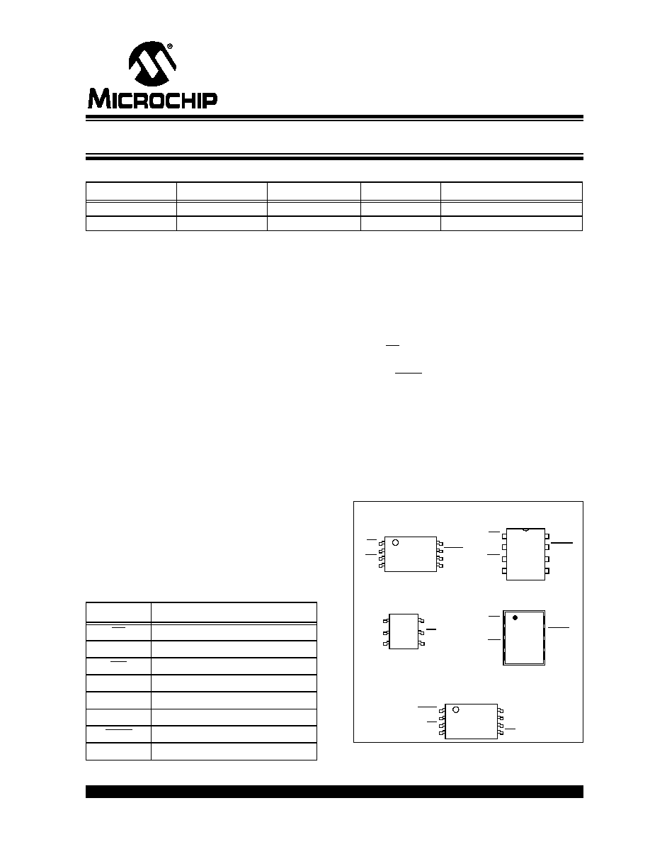
The 25XX040A is available in standard packages
including 8-lead PDIP and SOIC, and advanced
packages including 8-lead MSOP, 8-lead TSSOP
and rotated TSSOP, 8-lead 2x3 DFN, and 6-lead
SOT-23.
Package Types (not to scale)
Part Number
V
CC
Range
Page Size
Temp. Ranges
Packages
25AA040A
1.8-5.5V
16 Bytes
I
P, MS, SN, ST, MC, OT
25LC040A
2.5-5.5V
16 Bytes
I, E
P, MS, SN, ST, MC, OT
- Industrial (I):
-40
∞
C to
+85
∞
C
- Automotive (E):
-40
∞
C to +125
∞
C
Name
Function
CS
Chip Select Input
SO
Serial Data Output
WP
Write-Protect
V
SS
Ground
SI
Serial Data Input
SCK
Serial Clock Input
HOLD
Hold Input
V
CC
Supply Voltage
CS
SO
WP
V
SS
1
2
3
4
8
7
6
5
V
CC
HOLD
SCK
SI
PDIP/SOIC
(P, SN)
CS
SO
WP
V
SS
1
2
3
4
8
7
6
5
V
CC
HOLD
SCK
SI
CS
SO
WP
V
SS
1
2
3
4
8
7
6
5
V
CC
HOLD
SCK
SI
TSSOP/MSOP
(ST, MS)
X-Rotated TSSOP
HOLD
V
CC
CS
SO
1
2
3
4
8
7
6
5
SCK
SI
V
SS
WP
(X/ST)
V
SS
1
2
3
4
6
5
V
DD
CS
SO
(OT)
SOT-23
SCK
SI
CS
SO
WP
V
SS
1
2
3
4
8
7
6
5
V
CC
HOLD
SCK
SI
(MC)
DFN
4K SPI Bus Serial EEPROM
*25XX040A is used in this document as a generic part number for the
25AA040A and the 25LC040A.
25AA040A/25LC040A
DS21827C-page 2
Preliminary
©
2006 Microchip Technology Inc.
1.0
ELECTRICAL CHARACTERISTICS
Absolute Maximum Ratings
()
V
CC
.............................................................................................................................................................................6.5V
All inputs and outputs w.r.t. V
SS
......................................................................................................... -0.6V to V
CC
+1.0V
Storage temperature .................................................................................................................................-65∞C to 150∞C
Ambient temperature under bias ...............................................................................................................-40∞C to 125∞C
ESD protection on all pins .......................................................................................................................................... 4 kV
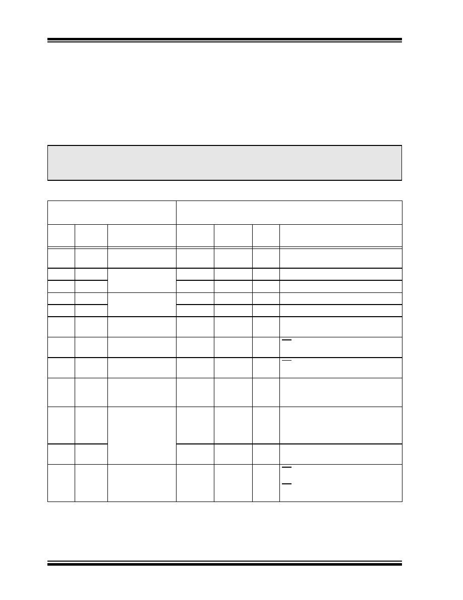
TABLE 1-1:
DC CHARACTERISTICS
NOTICE: Stresses above those listed under "Absolute Maximum Ratings" may cause permanent damage to the
device. This is a stress rating only and functional operation of the device at those or any other conditions above those
indicated in the operational listings of this specification is not implied. Exposure to maximum rating conditions for an
extended period of time may affect device reliability.
DC CHARACTERISTICS
Industrial (I):
T
A
= -40∞C to +85∞C
V
CC
= 1.8V to 5.5V
Automotive (E):
T
A
= -40∞C to +125∞C
V
CC
= 2.5V to 5.5V
Param.
No.
Sym.
Characteristic
Min.
Max.
Units
Test Conditions
D001
V
IH1
High-level Input
Voltage
0.7 V
CC
V
CC
+1
V
D002
V
IL1
Low-level Input
Voltage
-0.3
0.3 V
CC
V
V
CC
2.7V (Note 1)
D003
V
IL2
-0.3
0.2 V
CC
V
V
CC
< 2.7V (Note 1)
D004
V
OL
Low-level Output
Voltage
--
0.4
V
I
OL
= 2.1 mA
D005
V
OL
--
0.2
V
I
OL
= 1.0 mA, V
CC
< 2.5V
D006
V
OH
High-level Output
Voltage
V
CC
-0.5
--
V
I
OH
= -400
A
D007
I
LI
Input Leakage
Current
--
±1
A
CS = V
CC
, V
IN
= V
SS
TO
V
CC
D008
I
LO
Output Leakage
Current
--
±1
A
CS = V
CC
, V
OUT
= V
SS
TO
V
CC
D009
C
INT
Internal Capacitance
(all inputs and
outputs)
--
7
pF
T
A
= 25∞C, CLK = 1.0 MHz,
V
CC
= 5.0V (Note 1)
D010
I
CC
Read
Operating Current
--
--
5
2.5
mA
mA
V
CC
= 5.5V; F
CLK
= 10.0 MHz;
SO = Open
V
CC
= 2.5V; F
CLK
= 5.0 MHz;
SO = Open
D011
I
CC
Write
--
--
5
3
mA
mA
V
CC
= 5.5V
V
CC
= 2.5V
D012
I
CCS
Standby Current
--
--
5
1
A
A
CS = V
CC
= 5.5V, Inputs tied to V
CC
or
V
SS
, T
A
= +125∞C
CS = V
CC
= 2.5V, Inputs tied to V
CC
or
V
SS
, T
A
= +85∞C
Note 1: This parameter is periodically sampled and not 100% tested.
©
2006 Microchip Technology Inc.
Preliminary
DS21827C-page 3
25AA040A/25LC040A
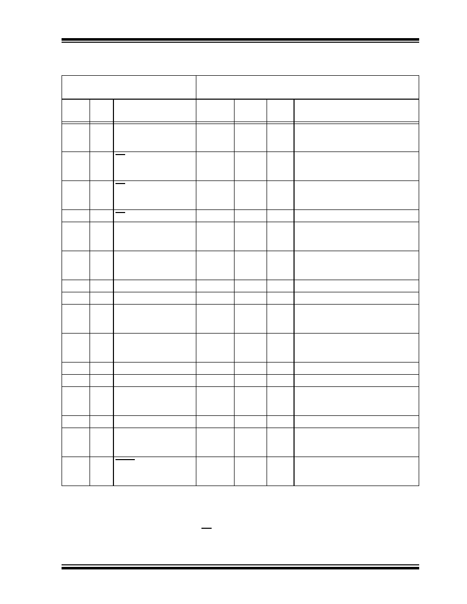
TABLE 1-2:
AC CHARACTERISTICS
AC CHARACTERISTICS
Industrial (I):
T
A
= -40∞C to +85∞C
V
CC
= 1.8V to 5.5V
Automotive (E): T
A
= -40∞C to +125∞C
V
CC
= 2.5V to 5.5V
Param.
No.
Sym.
Characteristic
Min.
Max.
Units
Test Conditions
1
F
CLK
Clock Frequency
--
--
--
10
5
3
MHz
MHz
MHz
4.5V
V
CC
<
5.5V
2.5V
V
CC
<
4.5V
1.8V
V
CC
<
2.5V
2
T
CSS
CS Setup Time
50
100
150
--
--
--
ns
ns
ns
4.5V
V
CC
<
5.5V
2.5V
V
CC
<
4.5V
1.8V
V
CC
<
2.5V
3
T
CSH
CS Hold Time
100
200
250
--
--
--
ns
ns
ns
4.5V
V
CC
<
5.5V
2.5V
V
CC
<
4.5V
1.8V
V
CC
<
2.5V
4
T
CSD
CS Disable Time
50
--
ns
--
5
Tsu
Data Setup Time
10
20
30
--
--
--
ns
ns
ns
4.5V
V
CC
<
5.5V
2.5V
V
CC
<
4.5V
1.8V
V
CC
<
2.5V
6
T
HD
Data Hold Time
20
40
50
--
--
--
ns
ns
ns
4.5V
V
CC
<
5.5V
2.5V
V
CC
<
4.5V
1.8V
V
CC
<
2.5V
7
T
R
CLK Rise Time
--
2
s
(Note 1)
8
T
F
CLK Fall Time
--
2
s
(Note 1)
9
T
HI
Clock High Time
0.05
0.1
0.15
1000
1000
1000
s
s
s
4.5V
V
CC
<
5.5V
2.5V
V
CC
<
4.5V
1.8V
V
CC
<
2.5V
10
T
LO
Clock Low Time
0.05
0.1
0.15
1000
1000
1000
s
s
s
4.5V
V
CC
<
5.5V
2.5V
V
CC
<
4.5V
1.8V
V
CC
<
2.5V
11
T
CLD
Clock Delay Time
50
--
ns
--
12
T
CLE
Clock Enable Time
50
--
ns
--
13
T
V
Output Valid from Clock
Low
--
--
--
50
100
160
ns
ns
ns
4.5V
V
CC
<
5.5V
2.5V
V
CC
<
4.5V
1.8V
V
CC
<
2.5V
14
T
HO
Output Hold Time
0
--
ns
(Note 1)
15
T
DIS
Output Disable Time
--
--
--
40
80
160
ns
ns
ns
4.5V
V
CC
<
5.5V (Note 1)
2.5V
V
CC
<
4.5V (Note 1)
1.8V
V
CC
<
2.5V (Note 1)
16
T
HS
HOLD Setup Time
20
40
80
--
--
--
ns
ns
ns
4.5V
V
CC
<
5.5V
2.5V
V
CC
<
4.5V
1.8V
V
CC
<
2.5V
Note 1: This parameter is periodically sampled and not 100% tested.
2: This parameter is not tested but ensured by characterization. For endurance estimates in a specific
application, please consult the Total EnduranceTM Model which can be obtained from our web site:
www.microchip.com.
3: T
WC
begins on the rising edge of CS after a valid write sequence and ends when the internal write cycle
is complete.
25AA040A/25LC040A
DS21827C-page 4
Preliminary
©
2006 Microchip Technology Inc.
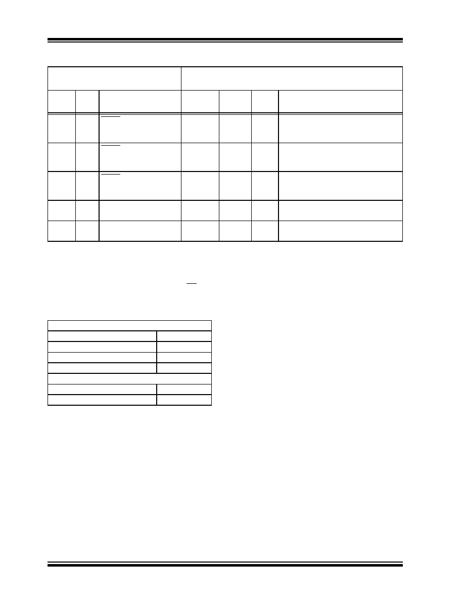
TABLE 1-3:
AC TEST CONDITIONS
17
T
HH
HOLD Hold Time
20
40
80
--
--
--
ns
ns
ns
4.5V
V
CC
<
5.5V
2.5V
V
CC
<
4.5V
1.8V
V
CC
<
2.5V
18
T
HZ
HOLD Low to Output
High-Z
30
60
160
--
--
--
ns
ns
ns
4.5V
V
CC
<
5.5V (Note 1)
2.5V
V
CC
<
4.5V (Note 1)
1.8V
V
CC
<
2.5V (Note 1)
19
T
HV
HOLD High to Output
Valid
30
60
160
--
--
--
ns
ns
ns
4.5V
V
CC
<
5.5V
2.5V
V
CC
<
4.5V
1.8V
V
CC
<
2.5V
20
T
WC
Internal Write Cycle Time
(byte or page)
--
5
ms
(N
OTE
3)
21
--
Endurance
1M
--
E/W
Cycles
(N
OTE
2)
TABLE 1-2:
AC CHARACTERISTICS (CONTINUED)
AC CHARACTERISTICS
Industrial (I):
T
A
= -40∞C to +85∞C
V
CC
= 1.8V to 5.5V
Automotive (E): T
A
= -40∞C to +125∞C
V
CC
= 2.5V to 5.5V
Param.
No.
Sym.
Characteristic
Min.
Max.
Units
Test Conditions
Note 1: This parameter is periodically sampled and not 100% tested.
2: This parameter is not tested but ensured by characterization. For endurance estimates in a specific
application, please consult the Total EnduranceTM Model which can be obtained from our web site:
www.microchip.com.
3: T
WC
begins on the rising edge of CS after a valid write sequence and ends when the internal write cycle
is complete.
AC Waveform:
V
LO
= 0.2V
--
V
H I
= V
CC
- 0.2V
(Note 1)
V
HI
= 4.0V
(Note 2)
C
L
= 100 pF
--
Timing Measurement Reference Level
Input
0.5 V
CC
Output
0.5 V
CC
Note 1: For V
CC
4.0V
2: For V
CC
4.0V
