©
1996 Microchip Technology Inc.
DS11126F-page 1
FEATURES
∑ Fast Read Access Time--150 ns
∑ CMOS Technology for Low Power Dissipation
- 30 mA Active
- 100
µ
A Standby
∑ Fast Byte Write Time--200
µ
s or 1 ms
∑ Data Retention >200 years
∑ Endurance - Minimum 10
4
Erase/Write Cycles
- Automatic Write Operation
- Internal Control Timer
- Auto-Clear Before Write Operation
- On-Chip Address and Data Latches
∑ Data Polling
∑ Chip Clear Operation
∑ Enhanced Data Protection
- V
CC
Detector
- Pulse Filter
- Write Inhibit
∑ 5-Volt-Only Operation
∑ Organized 512x8 JEDEC standard pinout
- 24-pin Dual-In-Line Package
- 32-pin PLCC Package
∑ Available for Extended Temperature Ranges:
- Commercial: 0∞C to +70∞C
- Industrial: -40∞C to +85∞C
DESCRIPTION
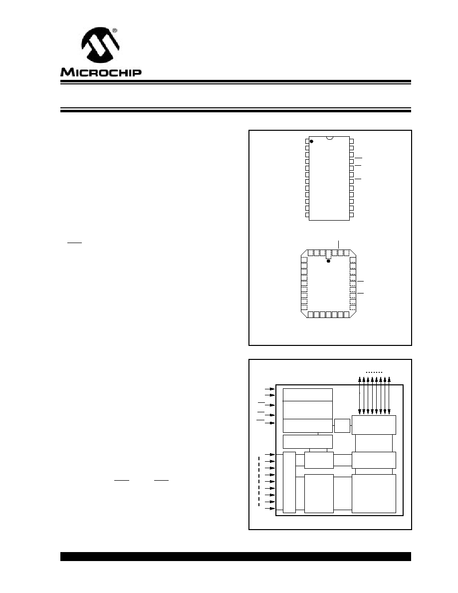
The Microchip Technology Inc. 28C04A is a CMOS 4K
non-volatile electrically Erasable and Programmable
Read Only Memory (EEPROM). The 28C04A is
accessed like a static RAM for the read or write cycles
without the need of external components. During a
"byte write", the address and data are latched internally,
freeing the microprocessor address and data bus for
other operations. Following the initiation of write cycle,
the device will go to a busy state and automatically
clear and write the latched data using an internal con-
trol timer. To determine when a write cycle is complete,
the 28C04A uses Data polling. Data polling allows the
user to read the location last written to when the write
operation is complete. CMOS design and processing
enables this part to be used in systems where reduced
power consumption and reliability are required. A com-
plete family of packages is offered to provide the utmost
flexibility in applications.
PACKAGE TYPES
BLOCK DIAGRAM
∑ 1
2
3
4
5
6
7
8
9
10
11
12
24
23
22
21
20
19
18
17
16
15
14
13
A7
A6
A5
A4
A3
A2
A1
A0
I/O0
I/O1
I/O2
V
Vcc
A8
NC
WE
OE
NC
CE
I/O7
I/O6
I/O5
I/O4
I/O3
SS
A6
A5
A4
A3
A2
A1
A0
NC
I/O0
A8
NC
NC
NC
OE
NC
CE
I/O7
I/O6
A7
NC
NC
NU
Vcc
WE
NC
I/O1
I/O2
Vss
NU
I/O3
I/O4
I/O5
14
15
16
17
18
19
20
4
3
2
1
32
31
30
29
28
27
26
25
24
23
22
21
5
6
7
8
9
10
11
12
13
DIP
PLCC
28C04A
∑ Pin 1 indicator on PLCC on top of package
28C04A
I/O0
I/O7
Input/Output
Buffers
Chip Enable/
Output Enable
Control Logic
CE
OE
Data Protection
Circuitry
A8
Y Gating
4K bit
Cell Matrix
X
Decoder
Y
Decoder
A0
Data
Poll
Auto Erase/Write
Timing
V
CC
V
SS
WE
L
a
t
c
h
e
s
Program Voltage
Generation
28C04A
4K (512 x 8) CMOS EEPROM
This document was created with FrameMaker 4 0 4
28C04A
DS11126F-page 2
©
1996 Microchip Technology Inc.
1.0
ELECTRICAL CHARACTERISTICS
1.1
MAXIMUM RATINGS*
V
CC
and input voltages w.r.t. V
SS
....... -0.6V to + 6.25V
Voltage on OE w.r.t. V
SS
...................... -0.6V to +13.5V
Output Voltage w.r.t. V
SS
.................-0.6V to V
CC
+0.6V
Storage temperature .......................... -65∞C to +125∞C
Ambient temp. with power applied ....... -50∞C to +95∞C
*Notice:
Stresses above those listed under "Maximum Ratings"
may cause permanent damage to the device. This is a stress rat-
ing only and functional operation of the device at those or any
other conditions above those indicated in the operation listings of
this specification is not implied. Exposure to maximum rating con-
ditions for extended periods may affect device reliability.
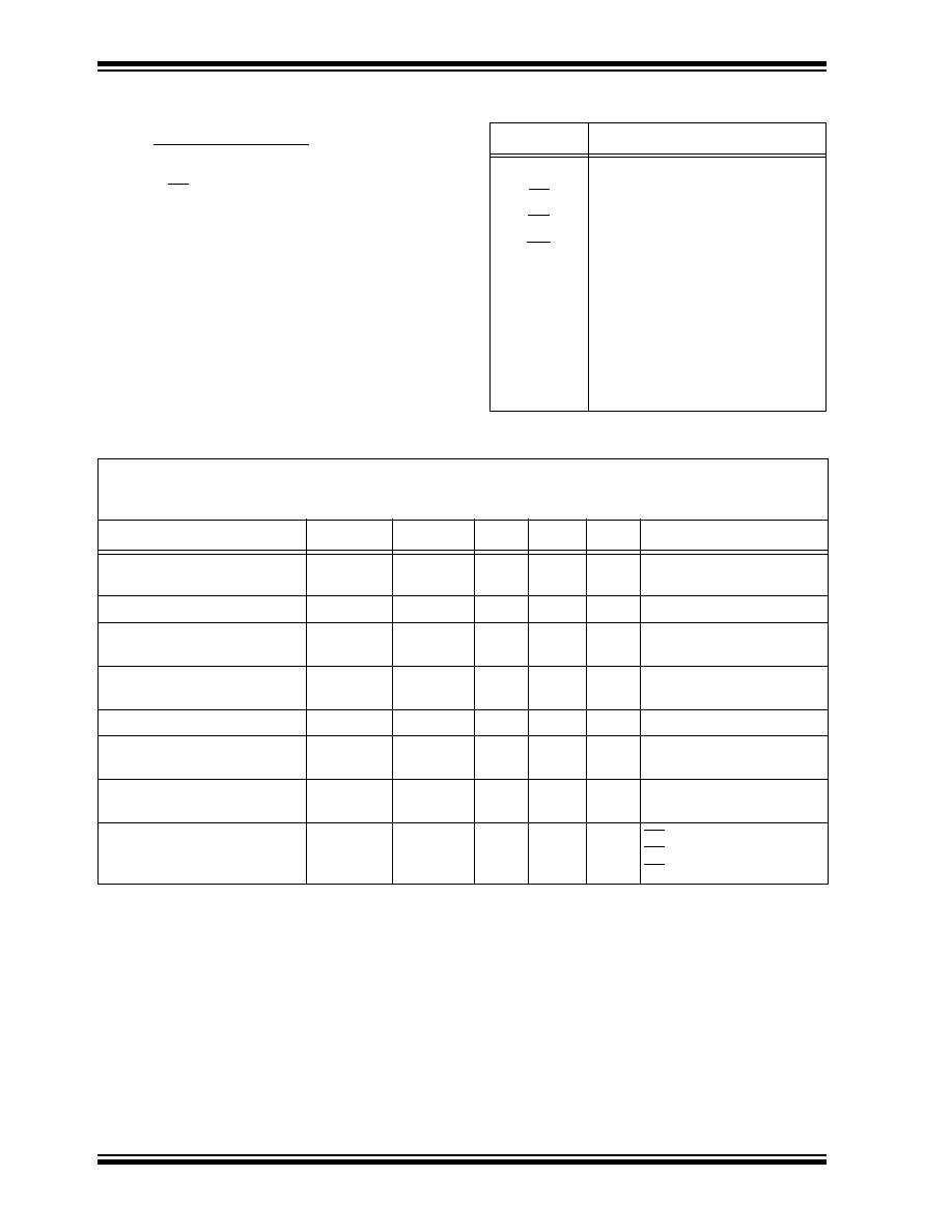
TABLE 1-1:
PIN FUNCTION TABLE
Name
Function
A0 - A8
Address Inputs
CE
Chip Enable
OE
Output Enable
WE
Write Enable
I/O0 - I/O7
Data Inputs/Outputs
V
CC
+5V Power Supply
V
SS
Ground
NC
No Connect; No Internal Connection
NU
Not Used; No External Connection is
Allowed
TABLE 1-2:
READ/WRITE OPERATION DC CHARACTERISTICS
V
CC
= +5V
±
10%
Commercial (C): Tamb =
0∞C to +70∞C
Industrial (I): Tamb = -40∞C to +85∞C
Parameter
Status
Symbol
Min
Max
Units
Conditions
Input Voltages
Logic `1'
Logic `0'
V
IH
V
IL
2.0
-0.1
V
CC
+1
0.8
V
V
Input Leakage
I
LI
-10
10
µ
A
V
IN
= -0.1V to V
CC
+1
Input Capacitance
C
IN
10
pF
V
IN
= 0V; Tamb = 25∞C;
f = 1 MHz
Output Voltages
Logic `1'
Logic `0'
V
OH
V
OL
2.4
0.45
V
V
I
OH
= -400
µ
A
I
OL
= 2.1 mA
Output Leakage
I
LO
-10
10
µ
A
V
OUT
= -0.1V
TO
V
CC
+ 0.1V
Output Capacitance
C
OUT
12
pF
V
IN
= 0V; T
AMB
= 25∞C;
f = 1 MHz
Power Supply Current, Active
TTL input
I
CC
30
mA
f = 5 MHz (Note 1)
V
CC
= 5.5V
Power Supply Current, Standby
TTL input
TTL input
CMOS input
I
CC
(
S
)
TTL
I
CC
(
S
)
TTL
I
CC
(
S
)
CMOS
2
3
100
mA
mA
µ
A
CE = V
IH
(0∞C to +70∞C)
CE = V
IH
(-40∞C to +85∞C)
CE = V
CC
-0.3 to Vcc+1
Note 1: AC power supply current above 5 MHz; 1 mA/MHz.
©
1996 Microchip Technology Inc.
DS11126F-page 3
28C04A
TABLE 1-3:
READ OPERATION AC CHARACTERISTICS
FIGURE 1-1:
READ WAVEFORMS
AC Testing Waveform:
V
IH
= 2.4V; V
IL
= 0.45V; V
OH
= 2.0V; V
OL
= 0.8V
Output Load:
1 TTL Load + 100 pF
Input Rise and Fall Times: 20 ns
Ambient Temperature:
Commercial (C): Tamb =
0∞C to +70∞C
Industrial
(I):
Tamb =
-40∞C to +85∞C
Parameter
Sym
28C04A-15
28C04A-20
28C04A-25
Units
Conditions
Min
Max
Min
Max
Min
Max
Address to Output Delay
t
ACC
150
200
250
ns
OE = CE = V
IL
CE to Output Delay
t
CE
150
200
250
ns
OE = V
IL
OE to Output Delay
t
OE
70
80
100
ns
CE = V
IL
CE to OE High Output Float
t
OFF
0
50
0
55
0
70
ns
Output Hold from Address, CE
or OE, whichever occurs first
t
OH
0
0
0
ns
Endurance
--
1M
--
1M
--
1M
--
cycles 25
∞
C, Vcc =
5.0V, Block
Mode (Note)
Note: This parameter is not tested but guaranteed by characterization. For endurance estimates in a specific applica-
tion, please consult the Total Endurance Model which can be obtained on our BBS or website.
Address
CE
V
IH
V
IL
V
IH
V
IL
V
IH
V
IL
OE
Data
WE
V
OH
V
OL
V
IH
V
IL
Address Valid
High Z
Valid Output
t
ACC
(1) t
OFF
is specified for OE or CE, whichever occurs first
(2) OE may be delayed up to t
CE
- t
OE
after the falling edge of CE without impact on t
CE
(3) This parameter is sampled and is not 100% tested
High Z
t
OH
t
OFF(1,3)
Notes:
t
OE(2)
t
CE(2)
28C04A
DS11126F-page 4
©
1996 Microchip Technology Inc.
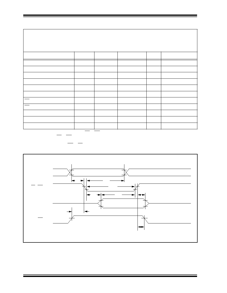
TABLE 1-4:
BYTE WRITE AC CHARACTERISTICS
FIGURE 1-2:
PROGRAMMING WAVEFORMS
AC Testing Waveform:
V
IH
= 2.4V; V
IL
= 0.45V; V
OH
= 2.0V; V
OL
= 0.8V
Output Load:
1 TTL Load + 100 pF
Input Rise/Fall Times:
20 nsec
Ambient Temperature:
Commercial (C): Tamb= 0∞C to 70∞C
Industrial
(I):
Tamb= -40∞C to 85∞C
Parameter
Symbol
Min
Max
Units
Remarks
Address Set-Up Time
t
AS
10
ns
Address Hold Time
t
AH
50
ns
Data Set-Up Time
t
DS
50
ns
Data Hold Time
t
DH
10
ns
Write Pulse Width
t
WPL
100
ns
Note 1
Write Pulse High Time
t
WPH
50
ns
OE Hold Time
t
OEH
10
ns
OE Set-Up Time
t
OES
10
ns
Data Valid Time
t
DV
1000
ns
Note 2
Write Cycle Time (28C04A)
t
WC
1
ms
0.5 ms typical
Write Cycle Time (28C04AF)
t
WC
200
µ
s
100
µ
s typical
Note 1: A write cycle can be initiated be CE or WE going low, whichever occurs last. The data is latched on the pos-
itive edge of CE or WE, whichever occurs first.
2: Data must be valid within 1000ns max. after a write cycle is initiated and must be stable at least until t
DH
after
the positive edge of WE or CE, whichever occurs first.
t
AS
t
AH
t
WPL
t
DS
t
DH
t
OES
t
OEH
t
DV
Address
CE, WE
Data In
OE
V
IH
V
IL
V
IH
V
IL
V
IH
V
IL
V
IH
V
IL

©
1996 Microchip Technology Inc.
DS11126F-page 5
28C04A
FIGURE 1-3:
DATA POLLING WAVEFORMS
FIGURE 1-4:
CHIP CLEAR WAVEFORMS
Address Valid
Last Written
Address Valid
t
ACC
t
CE
t
WPL
t
WPH
t
DV
t
WC
t
OE
True Data Out
Data In
Valid
V
IH
V
IL
Data
OE
WE
CE
Address
I/O7 Out
V
IH
V
IL
V
IH
V
IL
V
IH
V
IL
V
IH
V
IL
V
H
V
IH
CE
OE
WE
t
S
t
H
t
W
t
S
= = 1
µ
s
t
H
= 10ms
t
W
V
IH
V
IL
V
IH
V
IL
= 12.0V
±
0.5V
V
H

28C04A
DS11126F-page 6
©
1996 Microchip Technology Inc.
2.0
DEVICE OPERATION
The Microchip Technology Inc. 28C04A has four basic
modes of operation--read, standby, write inhibit, and
byte write--as outlined in the following table.
2.1
Read Mode
The 28C04A has two control functions, both of which
must be logically satisfied in order to obtain data at the
outputs. Chip enable (CE) is the power control and
should be used for device selection. Output Enable
(OE) is the output control and is used to gate data to the
output pins independent of device selection. Assuming
that addresses are stable, address access time (t
ACC
)
is equal to the delay from CE to output (t
CE
). Data is
available at the output tOE after the falling edge of OE,
assuming that CE has been low and addresses have
been stable for at least t
ACC
-t
OE
.
2.2
Standby Mode
The 28C04A is placed in the standby mode by applying
a high signal to the CE input. When in the standby
mode, the outputs are in a high impedance state, inde-
pendent of the OE input.
2.3
Data Protection
In order to ensure data integrity, especially during criti-
cal power-up and power-down transitions, the following
enhanced data protection circuits are incorporated:
First, an internal V
CC
detect (3.3 volts typical) will inhibit
the initiation of non-volatile programming operation
when V
CC
is less than the V
CC
detect circuit trip.
Second, there is a WE filtering circuit that prevents WE
pulses of less than 10 ns duration from initiating a write
cycle.
Third, holding WE or CE high or OE low, inhibits a write
cycle during power-on and power-off (V
CC
).
Operation
Mode
CE
IE
WE
I/O
Read
L
L
H
D
OUT
Standby
H
X
X
High Z
Write Inhibit
H
X
X
High Z
Write Inhibit
X
L
X
High Z
Write Inhibit
X
X
H
High Z
Byte Write
L
H
L
D
IN
Byte Clear
Automatic Before Each "Write"
X = Any TTL level.
2.4
Write Mode
The 28C04A has a write cycle similar to that of a Static
RAM. The write cycle is completely self-timed and initi-
ated by a low going pulse on the WE pin. On the falling
edge of WE, the address information is latched. On ris-
ing edge, the data and the control pins (CE and OE) are
latched.
2.5
Data Polling
The 28C04A features Data polling to signal the comple-
tion of a byte write cycle. During a write cycle, an
attempted read of the last byte written results in the
data complement of I/O7 (I/O0 to I/O6 are indetermin-
able). After completion of the write cycle, true data is
available. Data polling allows a simple read/compare
operation to determine the status of the chip eliminating
the need for external hardware.
2.6
Chip Clear
All data may be cleared to 1's in a chip clear cycle by
raising OE to 12 volts and bringing the WE and CE low.
This procedure clears all data.
28C04A
©
1996 Microchip Technology Inc.
DS11126F-page 7
28C04A Product Identification System
To order or to obtain information, e.g., on pricing or delivery, please use the listed part numbers, and refer to the factory or the listed
sales offices.
Package:
L = Plastic Leaded Chip Carrier (PLCC)
P = Plastic DIP (600mill)
Temperature
Blank = 0
∞
C to +70
∞
C
Range:
I
= -40
∞
C to +85
∞
C
Access Time:
15
150 ns
20
200 ns
25
250 ns
Shipping:
Blank
Tube
T
Tape and Reel "L" only
Option:
Blank = twc = 1ms
F = twc = 200
µ
s
Device:
28C04A
512 x 8 CMOS EEPROM
28C04A
F
T
≠
15
I
/P

DS11126F-page 8
©
1996 Microchip Technology Inc.
Information contained in this publication regarding device applications and the like is intended through suggestion only and may be superseded by updates. No repre-
sentation or warranty is given and no liability is assumed by Microchip Technology Incorporated with respect to the accuracy or use of such information, or infringement
of patents or other intellectual property rights arising from such use or otherwise. Use of Microchip's products as critical components in life support systems is not autho-
rized except with express written approval by Microchip. No licenses are conveyed, implicitly or otherwise, under any intellectual property rights. The Microchip logo and
name are registered trademarks of Microchip Technology Inc. All rights reserved. All other trademarks mentioned herein are the property of their respective companies.
W
ORLDWIDE
S
ALES
& S
ERVICE
ASIA/PACIFIC
China
Microchip Technology
Unit 406 of Shanghai Golden Bridge Bldg.
2077 Yan'an Road West, Hongiao District
Shanghai, Peoples Republic of China
Tel: 86 21 6275 5700
Fax: 011 86 21 6275 5060
Hong Kong
Microchip Technology
RM 3801B, Tower Two
Metroplaza
223 Hing Fong Road
Kwai Fong, N.T. Hong Kong
Tel: 852 2 401 1200 Fax: 852 2 401 3431
India
Microchip Technology
No. 6, Legacy, Convent Road
Bangalore 560 025 India
Tel: 91 80 526 3148 Fax: 91 80 559 9840
Korea
Microchip Technology
168-1, Youngbo Bldg. 3 Floor
Samsung-Dong, Kangnam-Ku,
Seoul, Korea
Tel: 82 2 554 7200 Fax: 82 2 558 5934
Singapore
Microchip Technology
200 Middle Road
#10-03 Prime Centre
Singapore 188980
Tel: 65 334 8870 Fax: 65 334 8850
Taiwan, R.O.C
Microchip Technology
10F-1C 207
Tung Hua North Road
Taipei, Taiwan, ROC
Tel: 886 2 717 7175 Fax: 886 2 545 0139
EUROPE
United Kingdom
Arizona Microchip Technology Ltd.
Unit 6, The Courtyard
Meadow Bank, Furlong Road
Bourne End, Buckinghamshire SL8 5AJ
Tel: 44 1628 850303 Fax: 44 1628 850178
France
Arizona Microchip Technology SARL
Zone Industrielle de la Bonde
2 Rue du Buisson aux Fraises
91300 Massy - France
Tel: 33 1 69 53 63 20 Fax: 33 1 69 30 90 79
Germany
Arizona Microchip Technology GmbH
Gustav-Heinemann-Ring 125
D-81739 Muenchen, Germany
Tel: 49 89 627 144 0 Fax: 49 89 627 144 44
Italy
Arizona Microchip Technology SRL
Centro Direzionale Colleone Pas Taurus 1
Viale Colleoni 1
20041 Agrate Brianza
Milan Italy
Tel: 39 39 6899939 Fax: 39 39 689 9883
JAPAN
Microchip Technology Intl. Inc.
Benex S-1 6F
3-18-20, Shin Yokohama
Kohoku-Ku, Yokohama
Kanagawa 222 Japan
Tel: 81 45 471 6166 Fax: 81 45 471 6122
9/3/96
AMERICAS
Corporate Office
Microchip Technology Inc.
2355 West Chandler Blvd.
Chandler, AZ 85224-6199
Tel: 602 786-7200 Fax: 602 786-7277
Technical Support: 602 786-7627
Web: http://www.microchip.com
Atlanta
Microchip Technology Inc.
500 Sugar Mill Road, Suite 200B
Atlanta, GA 30350
Tel: 770 640-0034 Fax: 770 640-0307
Boston
Microchip Technology Inc.
5 Mount Royal Avenue
Marlborough, MA 01752
Tel: 508 480-9990 Fax: 508 480-8575
Chicago
Microchip Technology Inc.
333 Pierce Road, Suite 180
Itasca, IL 60143
Tel: 708 285-0071 Fax: 708 285-0075
Dallas
Microchip Technology Inc.
14651 Dallas Parkway, Suite 816
Dallas, TX 75240-8809
Tel: 972 991-7177 Fax: 972 991-8588
Dayton
Microchip Technology Inc.
Suite 150
Two Prestige Place
Miamisburg, OH 45342
Tel: 513 291-1654 Fax: 513 291-9175
Los Angeles
Microchip Technology Inc.
18201 Von Karman, Suite 1090
Irvine, CA 92612
Tel: 714 263-1888 Fax: 714 263-1338
New York
Microchip Technmgy Inc.
150 Motor Parkway, Suite 416
Hauppauge, NY 11788
Tel: 516 273-5305 Fax: 516 273-5335
San Jose
Microchip Technology Inc.
2107 North First Street, Suite 590
San Jose, CA 95131
Tel: 408 436-7950 Fax: 408 436-7955
Toronto
Microchip Technology Inc.
5925 Airport Road, Suite 200
Mississauga, Ontario L4V 1W1, Canada
Tel: 905 405-6279
Fax: 905 405-6253
All rights reserved.
©
1996, Microchip Technology Incorporated, USA. 9/96
Printed on recycled paper.