©
1996 Microchip Technology Inc.
DS11173E-page 1
27C512A
FEATURES
∑ High speed performance
∑ CMOS Technology for low power consumption
- 25 mA Active current
- 30
µ
A Standby current
∑ Factory programming available
∑ Auto-insertion-compatible plastic packages
∑ Auto ID aids automated programming
∑ High speed express programming algorithm
∑ Organized 64K x 8: JEDEC standard pinouts
- 28-pin Dual-in-line package
- 32-pin PLCC Package
- 28-pin SOIC package
- 28-pin TSOP package
- 28-pin VSOP package
- Tape and reel
∑ Data Retention > 200 years
∑ Available for the following temperature ranges
- Commercial:
0∞C to +70∞C
- Industrial:
-40∞C to +85∞C
- Automotive:
-40∞C to +125∞C
DESCRIPTION
The Microchip Technology Inc. 27C512A is a CMOS
512K bit electrically Programmable Read Only Memory
(EPROM). The device is organized into 64K words by
8 bits (64K bytes). Accessing individual bytes from an
address transition or from power-up (chip enable pin
going low) is accomplished in less than 90 ns. This
very high speed device allows the most sophisticated
microprocessors to run at full speed without the need
for WAIT states. CMOS design and processing enables
this part to be used in systems where reduced power
consumption and high reliability are requirements.
A complete family of packages is offered to provide the
most flexibility in applications. For surface mount appli-
cations, PLCC, VSOP, TSOP or SOIC packaging is
available. Tape or reel packaging is also available for
PLCC or SOIC packages.
PACKAGE TYPES
1
2
3
4
5
6
7
8
9
10
11
12
13
14
28
27
26
25
24
23
22
21
20
19
18
17
16
15
A15
A12
A7
A6
A5
A4
A3
A2
A1
A0
O0
O1
O2
V
SS
V
CC
A14
A13
A8
A9
A11
OE/V
PP
A10
CE
O7
O6
O5
O4
O3
A6
A5
A4
A3
A2
A1
A0
NC
O0
A8
A9
A11
NC
OE/V
PP
A10
CE
O7
O6
A7
A12
A15
NU
Vcc
A14
A13
O1
O2
V
NU
O3
O4
O5
SS
5
6
7
8
9
10
11
12
13
29
28
27
26
25
24
23
22
21
14
15
16
17
18
19
20
4
3
2
1
32
31
30
OE/V
PP
A11
A9
A8
A13
A14
V
CC
A15
A12
A7
A6
A5
A4
A3
A10
CE
D7
D6
D5
D4
D3
V
SS
D2
D1
D0
A0
A1
A2
1
2
3
4
5
6
7
8
9
10
11
12
13
14
28
27
26
25
24
23
22
21
20
19
18
17
16
15
A10
CE
21
20
19
V
SS
O2
14
13
12
OE/V
PP
A11
A9
A8
22
23
24
A15
A12
A7
1
2
3
4
5
25
26
27
28
6
7
A13
A14
V
CC
A6
A5
A4
A3
O7
O6
O5
O4
O3
O1
O0
A0
A1
A2
18
17
16
15
11
10
9
8
TSOP
27C512A
PLCC
DIP/SOIC
VSOP
27C512A
27C512A
27C512A
512K (64K x 8) CMOS EPROM
This document was created with FrameMaker 4 0 4
27C512A
DS11173E-page 2
©
1996 Microchip Technology Inc.
1.0
ELECTRICAL CHARACTERISTICS
1.1
Maximum Ratings*
V
CC
and input voltages w.r.t. V
SS
........ -0.6V to +7.25V
V
PP
voltage w.r.t. V
SS
during
programming ......................................... -0.6V to +14V
Voltage on A9 w.r.t. V
SS
...................... -0.6V to +13.5V
Output voltage w.r.t. V
SS
............... -0.6V to V
CC
+1.0V
Storage temperature .......................... -65∞C to +150∞C
Ambient temp. with power applied ..... -65∞C to +125∞C
*Notice: Stresses above those listed under "Maximum Ratings"
may cause permanent damage to the device. This is a stress rat-
ing only and functional operation of the device at those or any
other conditions above those indicated in the operation listings of
this specification is not implied. Exposure to maximum rating con-
ditions for extended periods may affect device reliability.
TABLE 1-1:
PIN FUNCTION TABLE
Name
Function
A0-A15
Address Inputs
CE
Chip Enable
OE/V
PP
Output Enable/Programming Voltage
O0 - O7
Data Output
V
CC
+5V Power Supply
V
SS
Ground
NC
No Connection; No Internal Connec-
tion
NU
Not Used; No External Connection is
Allowed
TABLE 1-2:
READ OPERATION DC CHARACTERISTICS
V
CC
= +5V
±
10%
Commercial:
Tamb = 0∞C to +70∞C
Industrial:
Tamb = -40∞C to +85∞C
Extended (Automotive):
Tamb = -40∞C to +125∞C
Parameter
Part*
Status
Symbol
Min
Max
Units
Conditions
Input Voltages
all
Logic "1"
Logic "0"
V
IH
V
IL
2.0
-0.5
V
CC
+1
0.8
V
V
Input Leakage
all
I
LI
-10
10
µ
A
V
IN
= 0 to V
CC
Output Voltages
all
Logic "1"
Logic "0"
V
OH
V
OL
2.4
0.45
V
V
I
OH
= - 400
µ
A
I
OL
= 2.1 mA
Output Leakage
all
--
I
LO
-10
10
µ
A
V
OUT
= 0V to V
CC
Input Capacitance
all
--
C
IN
--
6
pF
V
IN
= 0V; Tamb = 25
∞
C;
f = 1 MHz
Output Capacitance
all
--
C
OUT
--
12
pF
V
OUT
= 0V; Tamb = 25
∞
C;
f = 1 MHz
Power Supply Current,
Active
C
I, E
TTL input
TTL input
I
CC
I
CC
--
--
25
35
mA
mA
V
CC
= 5.5V
f = 1 MHz;
OE/V
PP
= CE = V
IL
;
I
OUT
= 0 mA;
V
IL
= -0.1 to 0.8V;
V
IH
= 2.0 to V
CC
;
Note 1
Power Supply Current,
Standby
C
I, E
all
TTL input
TTL input
CMOS input
I
CC
(
S
)
TLL
I
CC
(
S
)
TLL
I
CC
(
S
)
CMOS
--
--
--
1
2
30
mA
mA
µ
A
CE = Vcc
±
0.2V
* Parts: C=Commercial Temperature Range; I, E=Industrial and Extended Temperature Ranges
Note 1: Typical active current increases .75 mA per MHz up to operating frequency for all temperature ranges.
©
1996 Microchip Technology Inc.
DS11173E-page 3
27C512A
TABLE 1-3:
READ OPERATION AC CHARACTERISTICS
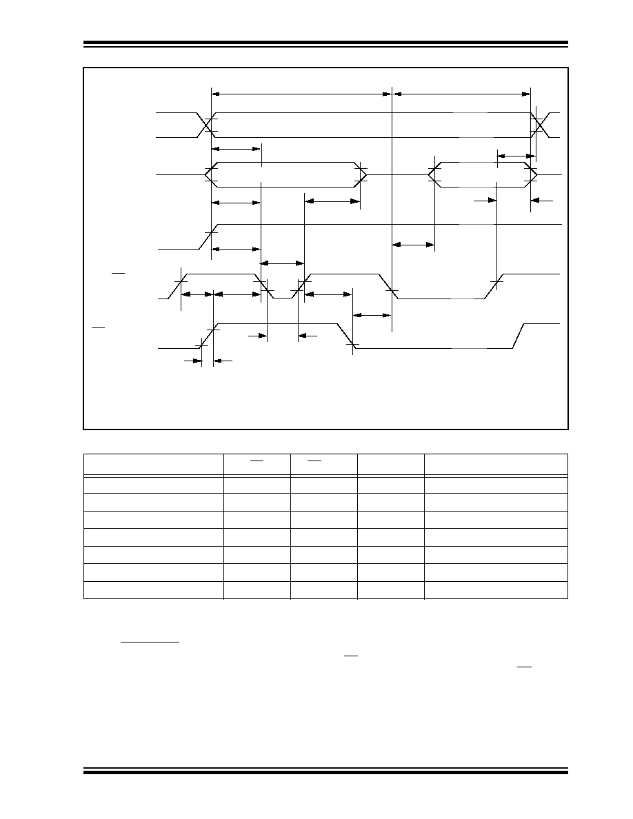
FIGURE 1-1:
READ WAVEFORMS
AC Testing Waveform:
V
IH
= 2.4V and V
IL
= .45V; V
OH
= 2.0V and V
OL
= 0.8V
Output Load:
1 TTL Load + 100 pF
Input Rise and Fall Times:
10 ns
Ambient Temperature:
Commercial:
Tamb = 0∞C to +70∞C
Industrial:
Tamb = -40∞C to +85∞C
Extended (Automotive):
Tamb = -40∞C to +125∞C
Parameter
Sym
27C512-90*
27C512-10*
27C512-12
27C512-15
Units Conditions
Min
Max
Min
Max
Min
Max
Min
Max
Address to Output
Delay
t
ACC
--
90
--
100
--
120
--
150
ns
CE = OE/
V
PP
= V
IL
CE to Output Delay
t
CE
--
90
--
100
--
120
--
150
ns
OE/V
PP
=
V
IL
OE to Output Delay
t
OE
--
40
--
40
--
50
--
60
ns
CE = V
IL
OE to Output High
Impedance
t
OFF
0
35
0
35
0
40
0
45
ns
Output Hold from
Address, CE or OE/
V
PP
, whichever
occurred first
t
OH
0
--
0
--
0
--
0
--
ns
*90/10 AC Testing Waveforms: V
IH
= 3.0V and V
IL
= 0V; V
OH
= 1.5V and V
OL
= 1.5V
Output Load: 1 TTL Load + 30 pF
Address
CE
V
IH
V
IL
V
IH
V
IL
V
IH
V
IL
OE
Outputs
O0 - O7
V
OH
V
OL
Address Valid
t
CE(2)
t
OE(2)
High Z
Valid Output
t
ACC
(1) t
OFF
is specified for OE or CE, whichever occurs first
(2) OE may be delayed up to t
CE
- t
OE
after the falling edge of CE without impact on t
CE
(3) This parameter is sampled and is not 100% tested.
High Z
t
OH
t
OFF(1,3)
Notes:
27C512A
DS11173E-page 4
©
1996 Microchip Technology Inc.
TABLE 1-4:
PROGRAMMING DC CHARACTERISTICS
TABLE 1-5:
PROGRAMMING AC CHARACTERISTICS
Ambient Temperature: Tamb = 25
∞
C
±
5
∞
C
V
CC
= 6.5V
±
0.25V, OE/V
PP
= V
H
= 13.0V
±
0.25V
Parameter
Status
Symbol
Min.
Max.
Units
Conditions (See Note 1)
Input Voltages
Logic "1"
Logic "0"
V
IH
V
IL
2.0
-0.1
V
CC
+1
0.8
V
V
Input Leakage
--
I
LI
-10
10
µ
A
V
IN
= 0V to V
CC
Output Voltages
Logic "1"
Logic "0"
V
OH
V
OL
2.4
--
0.45
V
V
I
OH
= -400
µ
A
I
OL
= 2.1 mA
V
CC
Current, program & verify
--
I
CC2
--
35
mA
CE = V
IL
OE/V
PP
Current, program
--
I
PP2
--
25
mA
A9 Product Identification
--
V
ID
11.5
12.5
V
Note 1: V
CC
must be applied simultaneously or before V
PP
voltage on OE/V
PP
and removed simultaneously or after
the V
PP
voltage on OE/V
PP
.
for Program, Program Verify
AC Testing Waveform:
V
IH
=2.4V and V
IL
=0.45V; V
OH
=2.0V; V
OL
=0.8V
and Program Inhibit Modes
Ambient Temperature:
25
∞
C
±
5
∞
C
V
CC
= 6.5V
±
0.25V, OE/V
PP
= V
H
= 13.0V
±
0.25 V
Parameter
Symbol
Min.
Max.
Units
Remarks
Address Set-Up Time
t
AS
2
--
µ
s
Data Set-Up Time
t
DS
2
--
µ
s
Data Hold Time
t
DH
2
--
µ
s
Address Hold Time
t
AH
0
--
µ
s
Float Delay (2)
t
DF
0
130
ns
V
CC
Set-Up Time
t
VCS
2
--
µ
s
Program Pulse Width (1)
t
PW
95
105
µ
s
100
µ
s typical
CE Set-Up Time
t
CES
2
--
µ
s
OE Set-Up Time
t
OES
2
--
µ
s
OE Hold Time
t
OEH
2
--
µ
s
OE Recovery Time
t
OR
2
--
µ
s
OE /V
PP
Rise Time During Programming
t
PRT
50
--
ns
Note 1: For express algorithm, initial programming width tolerance is 100
µ
s
±
5%.
2: This parameter is only sampled and not 100% teted. Output float is defined as the point where data is no
longer driven (see timing diagram).
©
1996 Microchip Technology Inc.
DS11173E-page 5
27C512A
FIGURE 1-2:
PROGRAMMING WAVEFORMS (1)
TABLE 1-6:
MODES
Operation Mode
CE
OE/V
PP
A9
O0 - O7
Read
V
IL
V
IL
X
D
OUT
Program
V
IL
V
H
X
D
IN
Program Verify
V
IL
V
IL
X
D
OUT
Program Inhibit
V
IH
V
H
X
High Z
Standby
V
IH
X
X
High Z
Output Disable
V
IL
V
IH
X
High Z
Identity
V
IL
V
IL
V
H
Identity Code
X = Don't Care
t
OPW
t
OEH
t
CE
(2)
V
IH
V
IL
V
IH
V
IL
6.5 V (3)
5.0V
V
IH
V
IL
Address
Data
V
CC
CE
Address Stable
t
DS
t
AS
Data In Stable
Data Out Valid
Verify
t
VCS
Notes:
The input timing reference level is 0.8V for V
IL
and 2.0V for V
IH
.
t
DF
and t
OE
are characteristics of the device but must be accommodated by the programmer.
V
CC
= 6.5V
±
0.25V, V
PP
= V
H
= 13.0V
±
0.5V for express programming algorithm.
(1)
(2)
(3)
t
DH
t
OR
t
DF
(2)
t
AH
t
PRT
t
CES
t
PW
t
OES
13.0 V (3)
V
IL
OE/V
PP
Program
1.2
Read Mode
(See Timing Diagrams and AC Characteristics)
Read Mode is accessed when
a)
the CE pin is low to power up (enable) the chip
b)
the OE/V
PP
pin is low to gate the data to the
output pins
For Read operations, if the addresses are stable, the
address access time (t
ACC
) is equal to the delay from
CE to output (t
CE
). Data is transferred to the output
after a delay (t
OE
) from the falling edge of OE/V
PP
.
27C512A
DS11173E-page 6
©
1996 Microchip Technology Inc.
1.3
Standby Mode
The standby mode is entered when the CE pin is high,
and the program mode is not identified.
When this conditions are met, the supply current will
drop from 25 mA to 30
µ
A.
1.4
Output Enable OE/V
PP
This multifunction pin eliminates bus connection in mul-
tiple bus microprocessor systems and the outputs go to
high impedance when:
∑ the OE/V
PP
pin is high (V
IH
).
When a V
H
input is applied to this pin, it supplies the
programming voltage (V
PP
) to the device.
1.5
Erase Mode (UV Windowed Versions)
Windowed products offer the ability to erase the mem-
ory array. The memory matrix is erased to the all "1's"
state as a result of being exposed to ultraviolet light. To
ensure complete erasure, a dose of 15 watt-second/
cm
2
is required. This means that the device window
must be placed within one inch and directly underneath
an ultraviolet lamp with a wavelength of 2537 Ang-
stroms, intensity of 12,000 mW/cm
2
for approximately
40 minutes.
1.6
Programming Mode
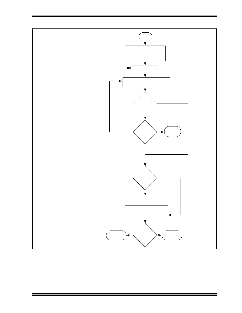
The Express algorithm must be used for best results. It
has been developed to improve programming yields
and throughput times in a production environment. Up
to 10 100-microsecond pulses are applied until the byte
is verified. A flowchart of the Express algorithm is
shown in Figure 1-3.
Programming takes place when:
a)
V
CC
is brought to the proper voltage,
b)
OE/V
PP
is brought to the proper V
H
level, and
c)
CE line is low.
Since the erased state is "1" in the array, programming
of "0" is required. The address to be programmed is set
via pins A0 - A15 and the data to be programmed is pre-
sented to pins O0 - O7. When data and address are
stable, a low going pulse on the CE line programs that
location.
1.7
Verify
After the array has been programmed it must be verified
to ensure all the bits have been correctly programmed.
This mode is entered when all the following conditions
are met:
a)
V
CC
is at the proper level,
b)
the OE/V
PP
pin is low, and
c)
the CE line is low.
1.8
Inhibit
When programming multiple devices in parallel with dif-
ferent data, only CE needs to be under separate control
to each device. By pulsing the CE line low on a partic-
ular device, that device will be programmed; all other
devices with CE held high will not be programmed with
the data (although address and data will be available on
their input pins).
1.9
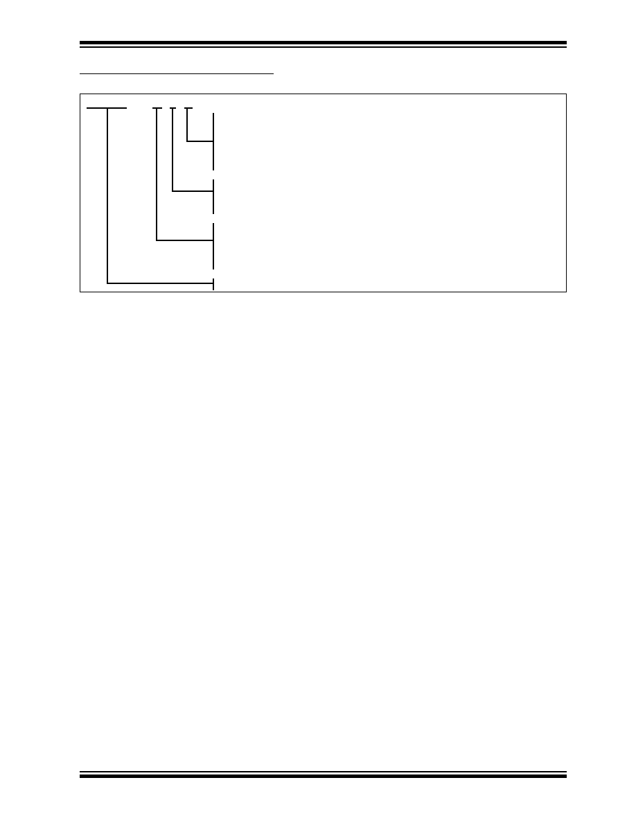
Identity Mode
In this mode specific data is output which identifies the
manufacturer as Microchip Technology Inc. and the
device type. This mode is entered when Pin A9 is taken
to V
H
(11.5V to 12.5V). The CE and OE/V
PP
lines must
be at V
IL
. A0 is used to access any of the two non-eras-
able bytes whose data appears on O0 through O7.
Pin
Input
Output
Identity
A0
0
7
O
6
O
5
O
4
O
3
O
2
O
1
O
0
H
e
x
Manufacturer
Device Type*
V
IL
V
IH
0
1
0
0
1
0
0
0
1
1
0
1
0
0
1
0
29
0D
* Code subject to change
©
1996 Microchip Technology Inc.
DS11173E-page 7
27C512A
FIGURE 1-3:
PROGRAMMING EXPRESS ALGORITHM
Start
ADDR = First Location
V
CC
= 6.5V
V
PP
= 13.0V
X = 0
Program one 100
µ
s pulse
Increment X
Verify
Byte
Pass
Fail
X = 10 ?
No
Yes
Device
Failed
Last
Address?
No
Increment Address
Conditions:
T
amb
= 25∞C
±
5∞C
V
CC
= 6.5
±
0.25V
V
PP
= 13.0
±
0.25V
Yes
V
CC
= V
PP
= 4.5V, 5.5V
Device
Passed
All
bytes
= original
data?
Device
Failed
No
Yes

27C512A
DS11173E-page 8
©
1996 Microchip Technology Inc.
NOTES:

©
1996 Microchip Technology Inc.
DS11173E-page 9
27C512A
NOTES:

27C512A
DS11173E-page 10
©
1996 Microchip Technology Inc.
NOTES:
27C512A
©
1996 Microchip Technology Inc.
DS11173E-page 11
27C512A Product Identification System
To order or to obtain information (e.g., on pricing or delivery),, please use listed part numbers, and refer to factory or listed sales offices.
Package:
L =
Plastic Leaded Chip Carrier
P =
Plastic DIP (600 Mil)
SO =
Plastic SOIC (300 Mil)
TS =
Thin Small Outline Package(TSOP) 8x20mm
VS =
Very Small Outline Package(VSOP) 8x13.4mm
Temperature
Blank =
0∞C to +70∞C
Range:
I
=
-40∞C to +85∞C
E =
-40∞C to +125∞C
Access
90 =
90 ns
Time:
10 =
100 ns
12 =
120 ns
15 =
150 ns
Device:
27C512A
512K (64K x 8) CMOS EPROM
27C512A ≠
70
I
/P

DS11173E-page 12
©
1996 Microchip Technology Inc.
Information contained in this publication regarding device applications and the like is intended through suggestion only and may be superseded by updates. No repre-
sentation or warranty is given and no liability is assumed by Microchip Technology Incorporated with respect to the accuracy or use of such information, or infringement
of patents or other intellectual property rights arising from such use or otherwise. Use of Microchip's products as critical components in life support systems is not autho-
rized except with express written approval by Microchip. No licenses are conveyed, implicitly or otherwise, under any intellectual property rights. The Microchip logo and
name are registered trademarks of Microchip Technology Inc. All rights reserved. All other trademarks mentioned herein are the property of their respective companies.
W
ORLDWIDE
S
ALES
& S
ERVICE
ASIA/PACIFIC
China
Microchip Technology
Unit 406 of Shanghai Golden Bridge Bldg.
2077 Yan'an Road West, Hongiao District
Shanghai, Peoples Republic of China
Tel: 86 21 6275 5700
Fax: 011 86 21 6275 5060
Hong Kong
Microchip Technology
RM 3801B, Tower Two
Metroplaza
223 Hing Fong Road
Kwai Fong, N.T. Hong Kong
Tel: 852 2 401 1200 Fax: 852 2 401 3431
India
Microchip Technology
No. 6, Legacy, Convent Road
Bangalore 560 025 India
Tel: 91 80 526 3148 Fax: 91 80 559 9840
Korea
Microchip Technology
168-1, Youngbo Bldg. 3 Floor
Samsung-Dong, Kangnam-Ku,
Seoul, Korea
Tel: 82 2 554 7200 Fax: 82 2 558 5934
Singapore
Microchip Technology
200 Middle Road
#10-03 Prime Centre
Singapore 188980
Tel: 65 334 8870 Fax: 65 334 8850
Taiwan, R.O.C
Microchip Technology
10F-1C 207
Tung Hua North Road
Taipei, Taiwan, ROC
Tel: 886 2 717 7175 Fax: 886 2 545 0139
EUROPE
United Kingdom
Arizona Microchip Technology Ltd.
Unit 6, The Courtyard
Meadow Bank, Furlong Road
Bourne End, Buckinghamshire SL8 5AJ
Tel: 44 1628 850303 Fax: 44 1628 850178
France
Arizona Microchip Technology SARL
Zone Industrielle de la Bonde
2 Rue du Buisson aux Fraises
91300 Massy - France
Tel: 33 1 69 53 63 20 Fax: 33 1 69 30 90 79
Germany
Arizona Microchip Technology GmbH
Gustav-Heinemann-Ring 125
D-81739 Muenchen, Germany
Tel: 49 89 627 144 0 Fax: 49 89 627 144 44
Italy
Arizona Microchip Technology SRL
Centro Direzionale Colleone Pas Taurus 1
Viale Colleoni 1
20041 Agrate Brianza
Milan Italy
Tel: 39 39 6899939 Fax: 39 39 689 9883
JAPAN
Microchip Technology Intl. Inc.
Benex S-1 6F
3-18-20, Shin Yokohama
Kohoku-Ku, Yokohama
Kanagawa 222 Japan
Tel: 81 45 471 6166 Fax: 81 45 471 6122
9/3/96
AMERICAS
Corporate Office
Microchip Technology Inc.
2355 West Chandler Blvd.
Chandler, AZ 85224-6199
Tel: 602 786-7200 Fax: 602 786-7277
Technical Support: 602 786-7627
Web: http://www.microchip.com
Atlanta
Microchip Technology Inc.
500 Sugar Mill Road, Suite 200B
Atlanta, GA 30350
Tel: 770 640-0034 Fax: 770 640-0307
Boston
Microchip Technology Inc.
5 Mount Royal Avenue
Marlborough, MA 01752
Tel: 508 480-9990 Fax: 508 480-8575
Chicago
Microchip Technology Inc.
333 Pierce Road, Suite 180
Itasca, IL 60143
Tel: 708 285-0071 Fax: 708 285-0075
Dallas
Microchip Technology Inc.
14651 Dallas Parkway, Suite 816
Dallas, TX 75240-8809
Tel: 972 991-7177 Fax: 972 991-8588
Dayton
Microchip Technology Inc.
Suite 150
Two Prestige Place
Miamisburg, OH 45342
Tel: 513 291-1654 Fax: 513 291-9175
Los Angeles
Microchip Technology Inc.
18201 Von Karman, Suite 1090
Irvine, CA 92612
Tel: 714 263-1888 Fax: 714 263-1338
New York
Microchip Technmgy Inc.
150 Motor Parkway, Suite 416
Hauppauge, NY 11788
Tel: 516 273-5305 Fax: 516 273-5335
San Jose
Microchip Technology Inc.
2107 North First Street, Suite 590
San Jose, CA 95131
Tel: 408 436-7950 Fax: 408 436-7955
Toronto
Microchip Technology Inc.
5925 Airport Road, Suite 200
Mississauga, Ontario L4V 1W1, Canada
Tel: 905 405-6279
Fax: 905 405-6253
All rights reserved.
©
1996, Microchip Technology Incorporated, USA. 9/96
Printed on recycled paper.