©
1998 Microchip Technology Inc.
DS11020G-page 1
27LV256
FEATURES
∑ Wide voltage range 3.0V to 5.5V
∑ High speed performance
- 200 ns access time available at 3.0V
∑ CMOS Technology for low power consumption
- 8 mA Active current at 3.0V
- 20 mA Active current at 5.5V
- 100
µ
A Standby current
∑ Factory programming available
∑ Auto-insertion-compatible plastic packages
∑ Auto ID aids automated programming
∑ Separate chip enable and output enable controls
∑ High speed "Express" programming algorithm
∑ Organized 32K x 8: JEDEC standard pinouts
- 28-pin Dual-in-line package
- 32-pin PLCC package
- 28-pin SOIC package
- Tape and reel
∑ Data Retention > 200 years
∑ Available for the following temperature ranges:
- Commercial:
0∞C to +70∞C
- Industrial:
-40∞C to +85∞C
DESCRIPTION
The Microchip Technology Inc. 27LV256 is a low volt-
age (3.0 volt) CMOS EPROM designed for battery pow-
ered applications. The device is organized as a 32K x
8 (32K-Byte) non-volatile memory product. The
27LV256 consumes only 8 mA maximum of active cur-
rent during a 3.0 volt read operation therefore improv-
ing battery performance. This device is designed for
very low voltage applications where conventional 5.0
volt only EPROMS can not be used. Accessing individ-
ual bytes from an address transition or from power-up
(chip enable pin going low) is accomplished in less than
200 ns at 3.0V. This device allows systems designers
the ability to use low voltage non-volatile memory with
today's' low voltage microprocessors and peripherals in
battery powered applications.
A complete family of packages is offered to provide the
most flexibility in applications. For surface mount appli-
cations, PLCC or SOIC packaging is available. Tape
and reel packaging is also available for PLCC or SOIC
packages.
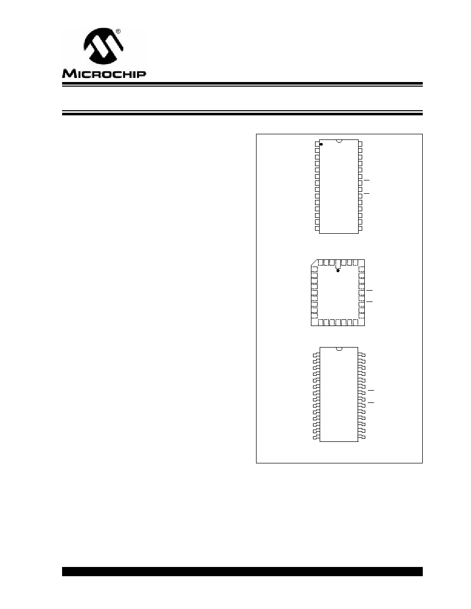
PACKAGE TYPES
∑ 1
2
3
4
5
6
7
8
9
10
11
12
13
14
28
27
26
25
24
23
22
21
20
19
18
17
16
15
V
A12
A7
A6
A5
A4
A3
A2
A1
A0
O0
O1
O2
V
V
A14
A13
A8
A9
A11
OE
A10
CE
O7
O6
O5
O4
O3
PP
SS
CC
A6
A5
A4
A3
A2
A1
A0
NC
O0
A8
A9
A11
NC
OE
A10
CE
O7
O6
A7
A12
V
NU
Vcc
A14
A13
O1
O2
V
NU
O3
O4
O5
PP
SS
5
6
7
8
9
10
11
12
13
29
28
27
26
25
24
23
22
21
14
15
16
17
18
19
20
4
3
2
1
32
31
30
1
2
3
4
5
6
7
8
9
10
11
12
13
14
28
27
26
25
24
23
22
21
20
19
18
17
16
15
V
PP
A12
A7
A6
A5
A4
A3
A2
A1
A0
O0
O1
O2
V
SS
V
CC
A14
A13
A8
A9
A11
OE
A10
CE
O7
O6
O5
O4
O3
PDIP
PLCC
SOIC
27L
V256
27L
V256
27L
V256
256K (32K x 8) Low-Voltage CMOS EPROM

27LV256
DS11020G-page 2
©
1998 Microchip Technology Inc.
1.0
ELECTRICAL
CHARACTERISTICS
1.1
Maximum Ratings*
V
CC
and input voltages w.r.t. V
SS
........ -0.6V to +7.25V
V
PP
voltage w.r.t. V
SS
during
programming ......................................... -0.6V to +14V
Voltage on A9 w.r.t. V
SS
....................... -0.6V to +13.5V
Output voltage w.r.t. V
SS
.................-0.6V to V
CC
+1.0V
Storage temperature .......................... -65∞C to +150∞C
Ambient temp. with power applied...... -65∞C to +125∞C
*Notice: Stresses above those listed under "Maximum Ratings"
may cause permanent damage to the device. This is a stress rat-
ing only and functional operation of the device at those or any
other conditions above those indicated in the operation listings of
this specification is not implied. Exposure to maximum rating con-
ditions for extended periods may affect device reliability.
TABLE 1-1:
PIN FUNCTION TABLE
Name
Function
A0-A14
Address Inputs
CE
Chip Enable
OE
Output Enable
V
PP
Programming Voltage
O0 - O7
Data Output
V
CC
+5V or +3V Power Supply
V
SS
Ground
NC
No Connection; No Internal
Connection
NU
Not Used; No External Connection Is
Allowed
TABLE 1-2:
READ OPERATION DC CHARACTERISTICS
V
CC
= +5V
±
10% or 3.0V where indicated
Commercial:
Tamb = 0∞C to +70∞C
Industrial:
Tamb = -40∞C to +85∞C
Parameter
Part*
Status
Symbol
Min.
Max.
Units
Conditions
Input Voltages
all
Logic "1"
Logic "0"
V
IH
V
IL
2.0
-0.5
V
CC
+1
0.8
V
V
Input Leakage
all
I
LI
-10
10
µ
A
V
IN
= 0 to V
CC
Output Voltages
all
Logic "1"
Logic "0"
V
OH
V
OL
2.4
0.45
V
V
I
OH
= -400
µ
A
I
OL
= 2.1 mA
Output Leakage
all
--
I
LO
-10
10
µ
A
V
OUT
= 0V to V
CC
Input Capacitance
all
--
C
IN
--
6
pF
V
IN
= 0V; Tamb = 25
∞
C;
f = 1 MHz
Output Capacitance
all
--
C
OUT
--
12
pF
V
OUT
= 0V; Tamb = 25
∞
C;
f = 1 MHz
Power Supply Current,
Active
C
I
TTL input
TTL input
I
CC1
I
CC2
--
--
20 @ 5.0V
8 @ 3.0V
25 @ 5.0V
10 @ 3.0V
mA
mA
mA
mA
V
CC
= 5.5V; V
PP
= V
CC
f = 1 MHz;
OE = CE = V
IL
;
I
OUT
= 0 mA;
V
IL
= -0.1 to 0.8V;
V
IH
= 2.0 to V
CC
;
Note 1
Power Supply Current,
Standby
C
I
all
TTL input
TTL input
CMOS input
I
CC
(
S
)
--
1 @ 3.0V
2 @ 3.0V
100 @ 3.0V
mA
mA
µ
A
CE=V
CC
±
0.2V
* Parts: C=Commercial Temperature Range
I =Industrial Temperature Ranges
Note 1: Typical active current increases .75 mA per MHz up to operating frequency for all temperature ranges.
©
1998 Microchip Technology Inc.
DS11020G-page 3
27LV256
TABLE 1-3:
READ OPERATION AC CHARACTERISTICS
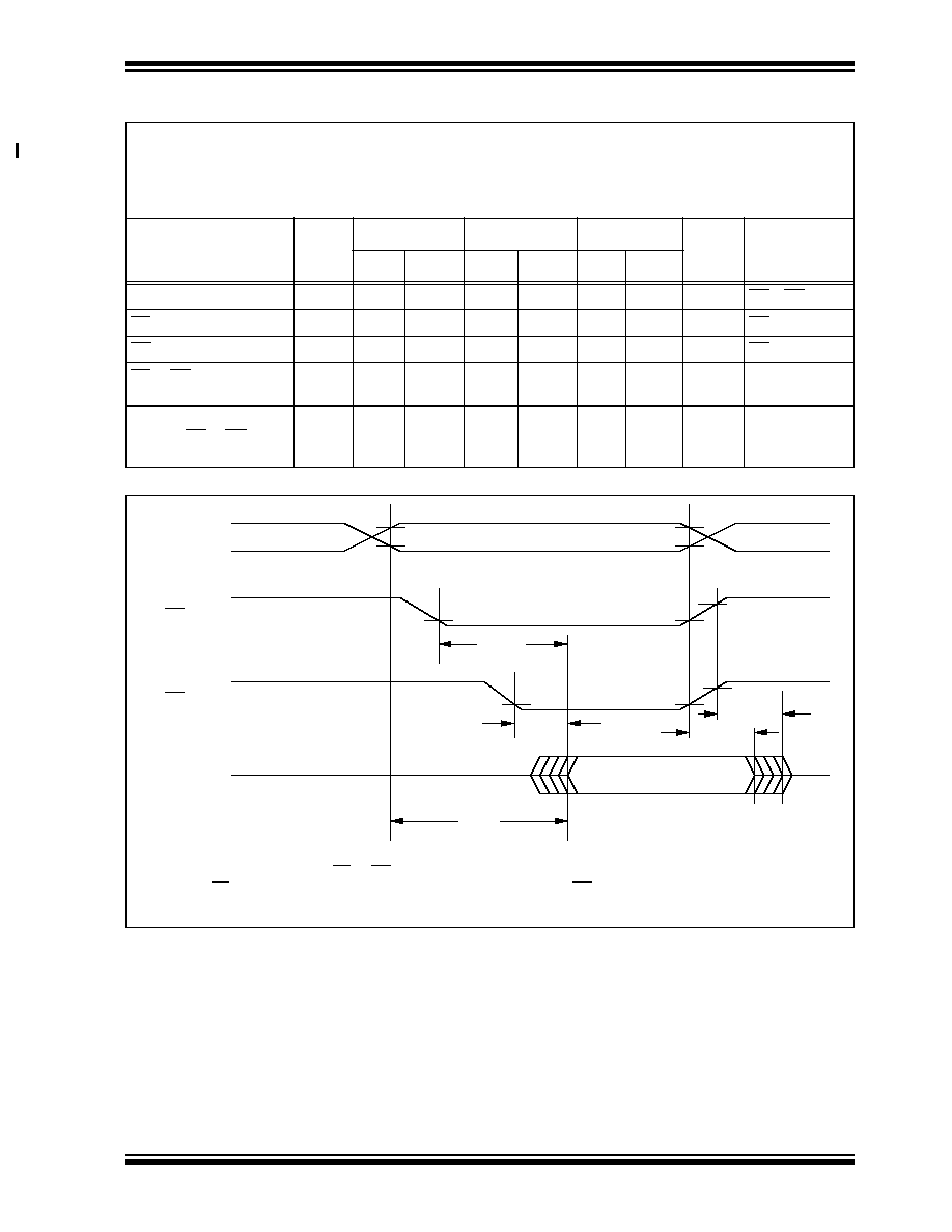
FIGURE 1-1:
READ WAVEFORMS
AC Testing Waveform:
V
IH
= 2.4V and V
IL
= 0.45V; V
OH
= 2.0V V
OL
= 0.8V
Output Load:
1 TTL Load + 100 pF
Input Rise and Fall Times: 10 ns
Ambient Temperature:
Commercial:
Tamb = 0∞C to +70∞C
Industrial:
Tamb = -40∞C to +85∞C
Parameter
Sym
27HC256-20
27HC256-25
27HC256-30
Units
Conditions
Min
Max
Min
Max
Min
Max
Address to Output Delay
t
ACC
--
200
--
250
--
300
ns
CE = OE = V
IL
CE to Output Delay
t
CE
--
200
--
250
--
300
ns
OE = V
IL
OE to Output Delay
t
OE
--
100
--
125
--
125
ns
CE = V
IL
CE or OE to O/P High
Impedance
t
OFF
0
50
0
50
0
50
ns
Output Hold from
Address CE or OE,
whichever goes first
t
OH
0
--
0
--
0
--
ns
Address
V
IH
V
IL
V
IH
V
IL
V
IH
V
IL
Outputs
O0 - O7
V
OH
V
OL
Address valid
t
CE(2)
t
OE(2)
High Z
Valid Output
t
ACC
(1) t
OFF
is specified for OE or CE, whichever occurs first
(2) OE may be delayed up to t
CE
- t
OE
after the falling edge of CE without impact on t
CE
(3) This parameter is sampled and is not 100% tested.
High Z
t
OH
t
OFF(1,3)
CE
OE
Notes:

27LV256
DS11020G-page 4
©
1998 Microchip Technology Inc.
TABLE 1-4:
PROGRAMMING DC CHARACTERISTICS
TABLE 1-5:
PROGRAMMING AC CHARACTERISTICS
Ambient Temperature: Tamb = 25
∞
C
±
5
∞
C
V
CC
= 6.5V
±
0.25V, V
PP
= 13.0V
±
0.25V
Parameter
Status
Symbol
Min
Max.
Units
Conditions
Input Voltages
Logic"1"
Logic"0"
V
IH
V
IL
2.0
-0.1
V
CC
+1
0.8
V
V
Input Leakage
--
I
LI
-10
10
µ
A
V
IN
= 0V to V
CC
Output Voltages
Logic"1"
Logic"0"
V
OH
V
OL
2.4
0.45
V
V
I
OH
= -400
µ
A
I
OL
= 2.1 mA
V
CC
Current, program & verify
--
I
CC2
--
20
mA
Note 1
V
PP
Current, program
--
I
PP2
--
25
mA
Note 1
A9 Product Identification
--
V
H
11.5
12.5
V
Note 1: V
CC
must be applied simultaneously or before V
PP
and removed simultaneously or after V
PP
.
for Program, Program Verify
AC Testing Waveform:
V
IH
=2.4V and V
IL
=0.45V; V
OH
=2.0V; V
OL
=0.8V
and Program Inhibit Modes
Output Load:
1 TLL Load + 100pF
Ambient Temperature:
Tamb=25
∞
C
±
5
∞
C
V
CC
= 6.5V
±
0.25V, V
PP
=13.0V
±
0.25V
Parameter
Symbol
Min.
Max.
Units
Remarks
Address Set-Up Time
t
AS
2
--
µ
s
Data Set-Up Time
t
DS
2
--
µ
s
Data Hold Time
t
DH
2
--
µ
s
Address Hold Time
t
AH
0
--
µ
s
Float Delay (2)
t
DF
0
130
ns
V
CC
Set-Up Time
t
VCS
2
--
µ
s
Program Pulse Width (1)
t
PW
95
105
µ
s
100
µ
s typical
CE Set-Up Time
t
CES
2
--
µ
s
OE Set-Up Time
t
OES
2
--
µ
s
V
PP
Set-Up Time
t
VPS
2
--
µ
s
Data Valid from OE
t
OE
--
100
ns
Note 1: For express algorithm, initial programming width tolerance is 100
µ
s
±
5%.
2: This parameter is only sampled and not 100% tested. Output float is defined as the point where data is no
longer driven (see timing diagram).

©
1998 Microchip Technology Inc.
DS11020G-page 5
27LV256
FIGURE 1-2:
PROGRAMMING WAVEFORMS
TABLE 1-6:
MODES
Operation Mode
CE
OE
V
PP
A9
O0 - O7
Read
V
IL
V
IL
V
CC
X
D
OUT
Program
V
IL
V
IH
V
H
X
D
IN
Program Verify
V
IH
V
IL
V
H
X
D
OUT
Program Inhibit
V
IH
V
IH
V
H
X
High Z
Standby
V
IH
X
V
CC
X
High Z
Output Disable
V
IL
V
IH
V
CC
X
High Z
Identity
V
IL
V
IL
V
CC
V
H
Identity Code
X = Don't Care
V
IH
V
IL
V
IH
V
IL
13.0V(2)
5.0V
6.5V(2)
5.0V
V
IH
V
IL
V
IH
V
IL
Address
Data
V
PP
V
CC
CE
OE
t
DF
and t
OE
are characteristics of the device but must be accommodated by the programmer
V
CC
= 6.5V
±
0.25V, V
PP
= V
H
= 13.0V
±
0.25V for express algorithm
t
PW
t
OPW
t
OES
Address Stable
t
AH
t
DS
t
VPS
t
DF
(1)
t
DH
t
OE
(1)
t
AS
Program
Data Stable
Data Out Valid
Verify
t
VCS
Notes:
(1)
(2)
High Z
1.2
Read Mode
(See Timing Diagrams and AC Characteristics)
Read Mode is accessed when:
a)
the CE pin is low to power up (enable) the chip
b)
the OE pin is low to gate the data to the output
pins
For Read operations, if the addresses are stable, the
address access time (t
ACC
) is equal to the delay from
CE to output (t
CE
). Data is transferred to the output
after a delay from the falling edge of OE (t
OE
).

27LV256
DS11020G-page 6
©
1998 Microchip Technology Inc.
1.3
Standby Mode
The standby mode is defined when the CE pin is high
(V
IH
) and a program mode is not defined. Output Dis-
able
1.4
Output Enable
This feature eliminates bus contention in multiple bus
microprocessor systems and the outputs go to a high
impedance when the following condition is true:
∑ The OE pin is high and program mode is not
defined.
1.5
Programming Mode
The Express algorithm has been developed to improve
on the programming throughput times in a production
environment. Up to 10 100-microsecond pulses are
applied until the byte is verified. No over-programming
is required. A flowchart of the express algorithm is
shown in Figure 1.
Programming takes place when:
a)
V
CC
is brought to the proper voltage
b)
V
PP
is brought to the proper V
H
level
c)
the OE pin is high
d)
the CE pin is low
Since the erased state is "1" in the array, programming
of "0" is required. The address to be programmed is set
via pins A0-A14 and the data to be programmed is pre-
sented to pins O0-O7. When data and address are sta-
ble, a low-going pulse on the CE line programs that
location.
1.6
Verify
After the array has been programmed it must be veri-
fied to ensure that all the bits have been correctly pro-
grammed. This mode is entered when all of the
following conditions are met:
a)
V
CC
is at the proper level
b)
V
PP
is at the proper V
H
level
c)
the CE pin is high
d)
the OE line is low
1.7
Inhibit
When Programming multiple devices in parallel with dif-
ferent data, only CE needs to be under separate control
to each device. By pulsing the CE line low on a partic-
ular device, that device will be programmed, and all
other devices with CE held high will not be programmed
with the data although address and data are available
on their input pins.
1.8
Identity Mode
In this mode specific data is outputted which identifies
the manufacturer as Microchip Technology Inc. and
device type. This mode is entered when Pin A9 is taken
to V
H
(11.5V to 12.5V). The CE and OE lines must be
at V
IL
. A0 is used to access any of the two non-eras-
able bytes whose data appears on O0 through O7.
Pin
Input
Output
Identity
A0
0
7
O
6
O
5
O
4
O
3
O
2
O
1
O
0
H
e
x
Manufacturer
Device Type*
V
IL
V
IH
0
1
0
0
1
0
0
0
1
1
0
1
0
0
1
0
29
8C
* Code subject to change.

©
1998 Microchip Technology Inc.
DS11020G-page 7
27LV256
FIGURE 1-3:
PROGRAMMING EXPRESS ALGORITHM
Start
ADDR = First Location
V
CC
= 6.5V
V
PP
= 13.0V
X = 0
Program one 100
µ
s pulse
Increment X
Verify
Byte
Pass
Fail
X = 10?
No
Yes
Device
Failed
Last
Address?
No
Increment Address
Conditions:
T
amb
= 25+/-5C
V
CC
= 6.5+/-0.25V
V
PP
= 13.0+/-0.25V
Yes
V
CC
= V
PP
= 4.5V, 5.5V
Device
Passed
All
bytes
= original
data?
Device
Failed
No
Yes

27LV256
DS11020G-page 8
©
1998 Microchip Technology Inc.
NOTES:

©
1998 Microchip Technology Inc.
DS11020G-page 9
27LV256
NOTES:

27LV256
DS11020G-page 10
©
1998 Microchip Technology Inc.
NOTES:

27LV256
27LV256 Product Identification System
To order or to obtain information, e.g., on pricing or delivery, please use the listed part numbers, and refer to the factory or the listed
sales offices.
Package:
L = Plastic Leaded Chip Carrier
P = Plastic DIP (600 Mil)
SO = Plastic SOIC (300 Mil)
Temperature
Blank = 0∞C to +70∞C
Range:
I
= -40∞C to +85∞C
Access
Time:
20 = 200 ns
25 = 250 ns
30 = 300 ns (SOIC only)
Device:
27LV256
256K (32K x 8) Low-Voltage CMOS EPROM
27LV256
≠
25
I
/P
©
1998 Microchip Technology Inc.
DS11020G-page 11

2002 Microchip Technology Inc.
Information contained in this publication regarding device
applications and the like is intended through suggestion only
and may be superseded by updates. It is your responsibility to
ensure that your application meets with your specifications.
No representation or warranty is given and no liability is
assumed by Microchip Technology Incorporated with respect
to the accuracy or use of such information, or infringement of
patents or other intellectual property rights arising from such
use or otherwise. Use of Microchip's products as critical com-
ponents in life support systems is not authorized except with
express written approval by Microchip. No licenses are con-
veyed, implicitly or otherwise, under any intellectual property
rights.
Trademarks
The Microchip name and logo, the Microchip logo, FilterLab,
K
EE
L
OQ
, microID, MPLAB, PIC, PICmicro, PICMASTER,
PICSTART, PRO MATE, SEEVAL and The Embedded Control
Solutions Company are registered trademarks of Microchip Tech-
nology Incorporated in the U.S.A. and other countries.
dsPIC, ECONOMONITOR, FanSense, FlexROM, fuzzyLAB,
In-Circuit Serial Programming, ICSP, ICEPIC, microPort,
Migratable Memory, MPASM, MPLIB, MPLINK, MPSIM,
MXDEV, PICC, PICDEM, PICDEM.net, rfPIC, Select Mode
and Total Endurance are trademarks of Microchip Technology
Incorporated in the U.S.A.
Serialized Quick Turn Programming (SQTP) is a service mark
of Microchip Technology Incorporated in the U.S.A.
All other trademarks mentioned herein are property of their
respective companies.
© 2002, Microchip Technology Incorporated, Printed in the
U.S.A., All Rights Reserved.
Printed on recycled paper.
Microchip received QS-9000 quality system
certification for its worldwide headquarters,
design and wafer fabrication facilities in
Chandler and Tempe, Arizona in July 1999. The
Company's quality system processes and
procedures are QS-9000 compliant for its
PICmicro
Æ
8-bit MCUs, K
EE
L
OQ
Æ
code hopping
devices, Serial EEPROMs and microperipheral
products. In addition, Microchip's quality
system for the design and manufacture of
development systems is ISO 9001 certified.
Note the following details of the code protection feature on PICmicro
Æ
MCUs.
∑
The PICmicro family meets the specifications contained in the Microchip Data Sheet.
∑
Microchip believes that its family of PICmicro microcontrollers is one of the most secure products of its kind on the market today,
when used in the intended manner and under normal conditions.
∑
There are dishonest and possibly illegal methods used to breach the code protection feature. All of these methods, to our knowl-
edge, require using the PICmicro microcontroller in a manner outside the operating specifications contained in the data sheet.
The person doing so may be engaged in theft of intellectual property.
∑
Microchip is willing to work with the customer who is concerned about the integrity of their code.
∑
Neither Microchip nor any other semiconductor manufacturer can guarantee the security of their code. Code protection does not
mean that we are guaranteeing the product as "unbreakable".
∑
Code protection is constantly evolving. We at Microchip are committed to continuously improving the code protection features of
our product.
If you have any further questions about this matter, please contact the local sales office nearest to you.

2002 Microchip Technology Inc.
M
AMERICAS
Corporate Office
2355 West Chandler Blvd.
Chandler, AZ 85224-6199
Tel: 480-792-7200 Fax: 480-792-7277
Technical Support: 480-792-7627
Web Address: http://www.microchip.com
Rocky Mountain
2355 West Chandler Blvd.
Chandler, AZ 85224-6199
Tel: 480-792-7966 Fax: 480-792-7456
Atlanta
500 Sugar Mill Road, Suite 200B
Atlanta, GA 30350
Tel: 770-640-0034 Fax: 770-640-0307
Boston
2 Lan Drive, Suite 120
Westford, MA 01886
Tel: 978-692-3848 Fax: 978-692-3821
Chicago
333 Pierce Road, Suite 180
Itasca, IL 60143
Tel: 630-285-0071 Fax: 630-285-0075
Dallas
4570 Westgrove Drive, Suite 160
Addison, TX 75001
Tel: 972-818-7423 Fax: 972-818-2924
Detroit
Tri-Atria Office Building
32255 Northwestern Highway, Suite 190
Farmington Hills, MI 48334
Tel: 248-538-2250 Fax: 248-538-2260
Kokomo
2767 S. Albright Road
Kokomo, Indiana 46902
Tel: 765-864-8360 Fax: 765-864-8387
Los Angeles
18201 Von Karman, Suite 1090
Irvine, CA 92612
Tel: 949-263-1888 Fax: 949-263-1338
New York
150 Motor Parkway, Suite 202
Hauppauge, NY 11788
Tel: 631-273-5305 Fax: 631-273-5335
San Jose
Microchip Technology Inc.
2107 North First Street, Suite 590
San Jose, CA 95131
Tel: 408-436-7950 Fax: 408-436-7955
Toronto
6285 Northam Drive, Suite 108
Mississauga, Ontario L4V 1X5, Canada
Tel: 905-673-0699 Fax: 905-673-6509
ASIA/PACIFIC
Australia
Microchip Technology Australia Pty Ltd
Suite 22, 41 Rawson Street
Epping 2121, NSW
Australia
Tel: 61-2-9868-6733 Fax: 61-2-9868-6755
China - Beijing
Microchip Technology Consulting (Shanghai)
Co., Ltd., Beijing Liaison Office
Unit 915
Bei Hai Wan Tai Bldg.
No. 6 Chaoyangmen Beidajie
Beijing, 100027, No. China
Tel: 86-10-85282100 Fax: 86-10-85282104
China - Chengdu
Microchip Technology Consulting (Shanghai)
Co., Ltd., Chengdu Liaison Office
Rm. 2401, 24th Floor,
Ming Xing Financial Tower
No. 88 TIDU Street
Chengdu 610016, China
Tel: 86-28-6766200 Fax: 86-28-6766599
China - Fuzhou
Microchip Technology Consulting (Shanghai)
Co., Ltd., Fuzhou Liaison Office
Unit 28F, World Trade Plaza
No. 71 Wusi Road
Fuzhou 350001, China
Tel: 86-591-7503506 Fax: 86-591-7503521
China - Shanghai
Microchip Technology Consulting (Shanghai)
Co., Ltd.
Room 701, Bldg. B
Far East International Plaza
No. 317 Xian Xia Road
Shanghai, 200051
Tel: 86-21-6275-5700 Fax: 86-21-6275-5060
China - Shenzhen
Microchip Technology Consulting (Shanghai)
Co., Ltd., Shenzhen Liaison Office
Rm. 1315, 13/F, Shenzhen Kerry Centre,
Renminnan Lu
Shenzhen 518001, China
Tel: 86-755-2350361 Fax: 86-755-2366086
Hong Kong
Microchip Technology Hongkong Ltd.
Unit 901-6, Tower 2, Metroplaza
223 Hing Fong Road
Kwai Fong, N.T., Hong Kong
Tel: 852-2401-1200 Fax: 852-2401-3431
India
Microchip Technology Inc.
India Liaison Office
Divyasree Chambers
1 Floor, Wing A (A3/A4)
No. 11, O'Shaugnessey Road
Bangalore, 560 025, India
Tel: 91-80-2290061 Fax: 91-80-2290062
Japan
Microchip Technology Japan K.K.
Benex S-1 6F
3-18-20, Shinyokohama
Kohoku-Ku, Yokohama-shi
Kanagawa, 222-0033, Japan
Tel: 81-45-471- 6166 Fax: 81-45-471-6122
Korea
Microchip Technology Korea
168-1, Youngbo Bldg. 3 Floor
Samsung-Dong, Kangnam-Ku
Seoul, Korea 135-882
Tel: 82-2-554-7200 Fax: 82-2-558-5934
Singapore
Microchip Technology Singapore Pte Ltd.
200 Middle Road
#07-02 Prime Centre
Singapore, 188980
Tel: 65-334-8870 Fax: 65-334-8850
Taiwan
Microchip Technology Taiwan
11F-3, No. 207
Tung Hua North Road
Taipei, 105, Taiwan
Tel: 886-2-2717-7175 Fax: 886-2-2545-0139
EUROPE
Denmark
Microchip Technology Nordic ApS
Regus Business Centre
Lautrup hoj 1-3
Ballerup DK-2750 Denmark
Tel: 45 4420 9895 Fax: 45 4420 9910
France
Microchip Technology SARL
Parc d'Activite du Moulin de Massy
43 Rue du Saule Trapu
Batiment A - ler Etage
91300 Massy, France
Tel: 33-1-69-53-63-20 Fax: 33-1-69-30-90-79
Germany
Microchip Technology GmbH
Gustav-Heinemann Ring 125
D-81739 Munich, Germany
Tel: 49-89-627-144 0 Fax: 49-89-627-144-44
Italy
Microchip Technology SRL
Centro Direzionale Colleoni
Palazzo Taurus 1 V. Le Colleoni 1
20041 Agrate Brianza
Milan, Italy
Tel: 39-039-65791-1 Fax: 39-039-6899883
United Kingdom
Arizona Microchip Technology Ltd.
505 Eskdale Road
Winnersh Triangle
Wokingham
Berkshire, England RG41 5TU
Tel: 44 118 921 5869 Fax: 44-118 921-5820
01/18/02
W
ORLDWIDE
S
ALES
AND
S
ERVICE