©
1998 Microchip Technology Inc.
DS11024E-page 1
27LV64
FEATURES
∑ Wide voltage range 3.0V to 5.5V
∑ High speed performance
- 200 ns access time available at 3.0V
∑ CMOS Technology for low power consumption
- 8 mA active current at 3.0V
- 20 mA active current at 5.5V
- 100
µ
A standby current
∑ Factory programming available
∑ Auto-insertion-compatible plastic packages
∑ Auto ID aids automated programming
∑ Separate chip enable and output enable controls
∑ High speed "express" programming algorithm
∑ Organized 8K x 8: JEDEC standard pinouts
- 28-pin Dual-in-line package
- 32-pin PLCC Package
- 28-pin SOIC package
- Tape and reel
∑ Available for the following temperature ranges:
- Commercial:
0∞C to +70∞C
- Industrial:
-40∞C to +85∞C
DESCRIPTION
The Microchip Technology Inc. 27LV64 is a low-voltage
(3.0 volt) CMOS EPROM designed for battery powered
applications. The device is organized as 8K x 8 (8K-
Byte) non-volatile memory product. The 27LV64 con-
sumes only 8mA maximum of active current during a
3.0 volt read operation therefore improving battery per-
formance. This device is designed for very low voltage
applications where conventional 5.0 volt only EPROMs
can not be used. Accessing individual bytes from an
address transition or from power-up (chip enable pin
going low) is accomplished in less than 200 ns at
3.0V.This device allows system designers the ability to
use low voltage non-volatile memory with today's low
voltage microprocessors and peripherals in battery
powered applications.
A complete family of packages is offered to provide the
most flexibility in applications. For surface mount appli-
cations, PLCC or SOIC packaging is available. Tape
and reel packaging is also available for PLCC or SOIC
packages.
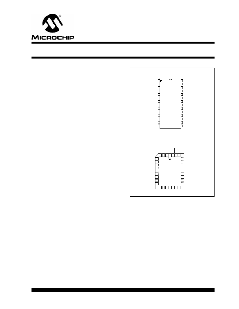
PACKAGE TYPES
∑ 1
2
3
4
5
6
7
8
9
10
11
12
13
14
28
27
26
25
24
23
22
21
20
19
18
17
16
15
V
A12
A7
A6
A5
A4
A3
A2
A1
A0
O0
O1
O2
V
V
PGM
NC
A8
A9
A11
OE
A10
CE
O7
O6
O5
O4
O3
PP
SS
CC
A6
A5
A4
A3
A2
A1
A0
NC
O0
A8
A9
A11
NC
OE
A10
CE
O7
O6
A7
A12
V
NU
Vcc
PGM
NC
O1
O2
V
NU
O3
O4
O5
PP
SS
5
6
7
8
9
10
11
12
13
29
28
27
26
25
24
23
22
21
14
15
16
17
18
19
20
4
3
2
1
32
31
30
DIP/SOIC
PLCC
27L
V64
27L
V64
64K (8K x 8) Low-Voltage CMOS EPROM

27LV64
DS11024E-page 2
©
1998 Microchip Technology Inc.
1.0
ELECTRICAL CHARACTERISTICS
1.1
Maximum Ratings*
V
CC
and input voltages w.r.t. V
SS
....... -0.6V to + 7.25V
V
PP
voltage w.r.t. V
SS
during
programming .......................................... -0.6V to +14V
Voltage on A9 w.r.t. V
SS
....................... -0.6V to +13.5V
Output voltage w.r.t. V
SS
.................-0.6V to V
CC
+1.0V
Storage temperature .......................... -65∞C to +150∞C
Ambient temp. with power applied...... -65∞C to +125∞C
*Notice: Stresses above those listed under "Maximum Ratings"
may cause permanent damage to the device. This is a stress rat-
ing only and functional operation of the device at those or any
other conditions above those indicated in the operation listings of
this specification is not implied. Exposure to maximum rating con-
ditions for extended periods may affect device reliability.
TABLE 1-1:
PIN FUNCTION TABLE
Name
Function
A0-A12
Address Inputs
CE
Chip Enable
OE
Output Enable
PGM
Program Enable
V
PP
Programming Voltage
O0 - O7
Data Output
V
CC
+5V Or +3V Power Supply
V
SS
Ground
NC
No Connection; No Internal Connec-
tions
NU
Not Used; No External Connection Is
Allowed
TABLE 1-2:
READ OPERATION DC CHARACTERISTICS
V
CC
= 3.0V to 5.5V unless otherwise specified
Commercial:
Tamb = 0∞C to +70∞C
Industrial:
Tamb = -40∞C to +85∞C
Parameter
Part*
Status
Symbol
Min.
Max.
Units
Conditions
Input Voltages
all
Logic "1"
Logic "0"
V
IH
V
IL
2.0
-0.5
V
CC
+1
0.8
V
V
Input Leakage
all
--
I
LI
-10
10
µ
A
V
IN
= 0 to V
CC
Output Voltages
all
Logic "1"
Logic "0"
V
OH
V
OL
2.4
0.45
V
V
I
OH
= -400
µ
A
I
OL
= 2.1 mA
Output Leakage
all
--
I
LO
-10
10
µ
A
V
OUT
= 0V to V
CC
Input Capacitance
all
--
C
IN
--
6
pF
V
IN
= 0V; Tamb = 25
∞
C;
f = 1 MHz
Output Capacitance
all
--
C
OUT
--
12
pF
V
OUT
= 0V; Tamb = 25
∞
C;
f = 1 MHz
Power Supply Current,
Active
C
I
TTL input
TTL input
I
CC1
I
CC2
--
--
20 @ 5.0V
8 @ 3.0V
25 @ 5.0V
10 @ 3.0V
mA
mA
mA
mA
V
CC
= 5.5V; V
PP
= V
CC
f = 1 MHz;
OE = CE = V
IL
;
I
OUT
= 0 mA;
V
IL
= -0.1 to 0.8V;
V
IH
= 2.0 to V
CC
;
Note 1
Power Supply Current,
Standby
C
I
all
TTL input
TTL input
CMOS input
I
CC
(
S
)
--
1 @ 3.0V
2@ 3.0V
100 @ 3.0V
mA
mA
µ
A
CE = V
CC
±
0.2V
* Parts: C=Commercial Temperature Range; I=Industrial Temperature Range
Note 1: Typical active current increases .5 mA per MHz up to operating frequency for all temperature ranges.

©
1998 Microchip Technology Inc.
DS11024E-page 3
27LV64
TABLE 1-3:
READ OPERATION AC CHARACTERISTICS
FIGURE 1-1:
READ WAVEFORMS
AC Testing Waveform:
V
IH
= 2.4V and V
IL
= 0.45V; V
OH
= 2.0V V
OL
= 0.8V
Output Load:
1 TTL Load + 100 pF
Input Rise and Fall Times:
10 ns
Ambient Temperature:
Commercial:
Tamb = 0∞C to +70∞C
Industrial:
Tamb = -40∞C to +85∞C
Parameter
Sym
27LV64-20
27LV64-25
27LV64-30
Units
Conditions
Min.
Max.
Min.
Max.
Min.
Max.
Address to Output Delay
t
ACC
--
200
--
250
--
300
ns
CE = OE = V
IL
CE to Output Delay
t
CE
--
200
--
250
--
300
ns
OE = V
IL
OE to Output Delay
t
OE
--
100
--
125
--
125
ns
CE = V
IL
CE or OE to O/P High
Impedance
t
OFF
0
50
0
50
0
50
ns
Output Hold from Address CE or
OE, whichever goes first
t
OH
0
--
0
--
0
--
ns
Address
CE
V
IH
V
IL
V
IH
V
IL
V
IH
V
IL
OE
Outputs
O0 - O7
V
OH
V
OL
Address Valid
t
CE(2)
t
OE(2)
High Z
Valid Output
t
ACC
(1) t
OFF
is specified for OE or CE, whichever occurs first
(2) OE may be delayed up to t
CE
- t
OE
after the falling edge of CE without impact on t
CE
(3) This parameter is sampled and is not 100% tested.
High Z
t
OH
t
OFF(1,3)
Notes:

27LV64
DS11024E-page 4
©
1998 Microchip Technology Inc.
TABLE 1-4:
PROGRAMMING DC CHARACTERISTICS
TABLE 1-5:
PROGRAMMING AC CHARACTERISTICS
Ambient Temperature: Tamb = 25
∞
C
±
5
∞
C
V
CC
= 6.5V
±
0.25V, V
PP
= V
H
= 13.0V
±
0.25V
Parameter
Status
Symbol
Min.
Max.
Units
Conditions
Input Voltages
Logic"1"
Logic"0"
V
IH
V
IL
2.0
-0.1
V
CC
+1
0.8
V
V
Input Leakage
--
I
LI
-10
10
µ
A
V
IN
= 0V to V
CC
Output Voltages
Logic"1"
Logic"0"
V
OH
V
OL
2.4
0.45
V
V
I
OH
= -400
µ
A
I
OL
= 2.1 mA
V
CC
Current, program & verify
--
I
CC2
--
20
mA
Note 1
V
PP
Current, program
--
I
PP2
--
25
mA
Note 1
A9 Product Identification
--
V
H
11.5
12.5
V
Note 1: V
CC
must be applied simultaneously or before V
PP
and removed simultaneously or after V
PP
.
for Program, Program Verify
AC Testing Waveform:
V
IH
=2.4V and V
IL
=0.45V; V
OH
=2.0V; V
OL
=0.8V
and Program Inhibit Modes
Ambient Temperature:
Tamb=25
∞
C
±
5
∞
C
V
CC
= 6.5V
±
0.25V, V
PP
= V
H
= 13.0V
±
0.25V
Parameter
Symbol
Min.
Max.
Units
Remarks
Address Set-Up Time
t
AS
2
--
µ
s
Data Set-Up Time
t
DS
2
--
µ
s
Data Hold Time
t
DH
2
--
µ
s
Address Hold Time
t
AH
0
--
µ
s
Float Delay (2)
t
DF
0
130
ns
V
CC
Set-Up Time
t
VCS
2
--
µ
s
Program Pulse Width (1)
t
PW
95
105
µ
s
100
µ
s typical
CE Set-Up Time
t
CES
2
--
µ
s
OE Set-Up Time
t
OES
2
--
µ
s
V
PP
Set-Up Time
t
VPS
2
--
µ
s
Data Valid from OE
t
OE
100
ns
Note 1: For express algorithm, initial programming width tolerance is 100
µ
s
±
5%.
Note 2: This parameter is only sampled and not 100% tested. Output float is defined as the point where data is no
longer driven (see timing diagram).

©
1998 Microchip Technology Inc.
DS11024E-page 5
27LV64
FIGURE 1-2:
PROGRAMMING WAVEFORMS (1)
TABLE 1-6:
MODES
Operation Mode
CE
OE
PGM
V
PP
A9
O0 - O7
Read
V
IL
V
IL
V
IH
V
CC
X
D
OUT
Program
V
IL
V
IH
V
IL
V
H
X
D
IN
Program Verify
V
IL
V
IL
V
IH
V
H
X
D
OUT
Program Inhibit
V
IH
X
X
V
H
X
High Z
Standby
V
IH
X
X
V
CC
X
High Z
Output Disable
V
IL
V
IH
V
IH
V
CC
X
High Z
Identity
V
IL
V
IL
V
IH
V
CC
V
H
Identity Code
X = Don't Care
V
IH
V
IL
V
IH
V
IL
13.0 V (3)
5.0 V
6.5 V (3)
5.0 V
V
IH
V
IL
V
IH
V
IL
V
IH
V
IL
Address
Data
V
PP
V
CC
CE
PGM
OE
Address Stable
t
AH
t
DS
t
DH
t
VPS
t
DF
(2)
t
AS
Program
Data In Stable
Data Out Valid
Verify
t
VCS
The input timing reference is 0.8V for V
IL
and 2.0V for V
IH
.
t
DF
and t
OE
are characteristics of the device but must be accommodated by the programmer.
Vcc = 6.5V
±
0.25V, V
PP
= V
H
= 13.0V
±
0.25V for Express algorithm.
Notes: (1)
(2)
(3)
t
PW
t
OPW
t
OES
t
OE
(2)
t
CES
High Z
1.2
Read Mode
(See Timing Diagrams and AC Characteristics)
Read Mode is accessed when
a)
the CE pin is low to power up (enable) the chip
b)
the OE pin is low to gate the data to the output
pins
For Read operations, if the addresses are stable, the
address access time (t
ACC
) is equal to the delay from
CE to output (t
CE
). Data is transferred to the output
after a delay from the falling edge of OE (t
OE
).


