
©
1998 Microchip Technology Inc.
DS11109J-page 1
FEATURES
∑ Fast Read Access Time--150 ns
∑ CMOS Technology for Low Power Dissipation
- 30 mA Active
- 100
µ
A Standby
∑ Fast Byte Write Time--200
µ
s or 1 ms
∑ Data Retention >200 years
∑ High Endurance - Minimum 100,000
Erase/Write
Cycles
∑ Automatic Write Operation
- Internal Control Timer
- Auto-Clear Before Write Operation
- On-Chip Address and Data Latches
∑ Data Polling
∑ Ready/Busy
∑ Chip Clear Operation
∑ Enhanced Data Protection
- V
CC
Detector
- Pulse Filter
- Write Inhibit
∑ Electronic Signature for Device Identification
∑ 5-Volt-Only Operation
∑ Organized 8Kx8 JEDEC Standard Pinout
- 28-pin Dual-In-Line Package
- 32-pin PLCC Package
- 28-pin SOIC Package
∑ Available for Extended Temperature Ranges:
- Commercial: 0∞C to +70∞C
- Industrial:
-40∞C to +85∞C
DESCRIPTION
The Microchip Technology Inc. 28C64A is a CMOS 64K non-
volatile electrically Erasable PROM. The 28C64A is
accessed like a static RAM for the read or write cycles without
the need of external components. During a "byte write", the
address and data are latched internally, freeing the micropro-
cessor address and data bus for other operations. Following
the initiation of write cycle, the device will go to a busy state
and automatically clear and write the latched data using an
internal control timer. To determine when the write cycle is
complete, the user has a choice of monitoring the Ready/
Busy output or using Data polling. The Ready/Busy pin is an
open drain output, which allows easy configuration in wired-
or systems. Alternatively, Data polling allows the user to read
the location last written to when the write operation is com-
plete. CMOS design and processing enables this part to be
used in systems where reduced power consumption and reli-
ability are required. A complete family of packages is offered
to provide the utmost flexibility in applications.
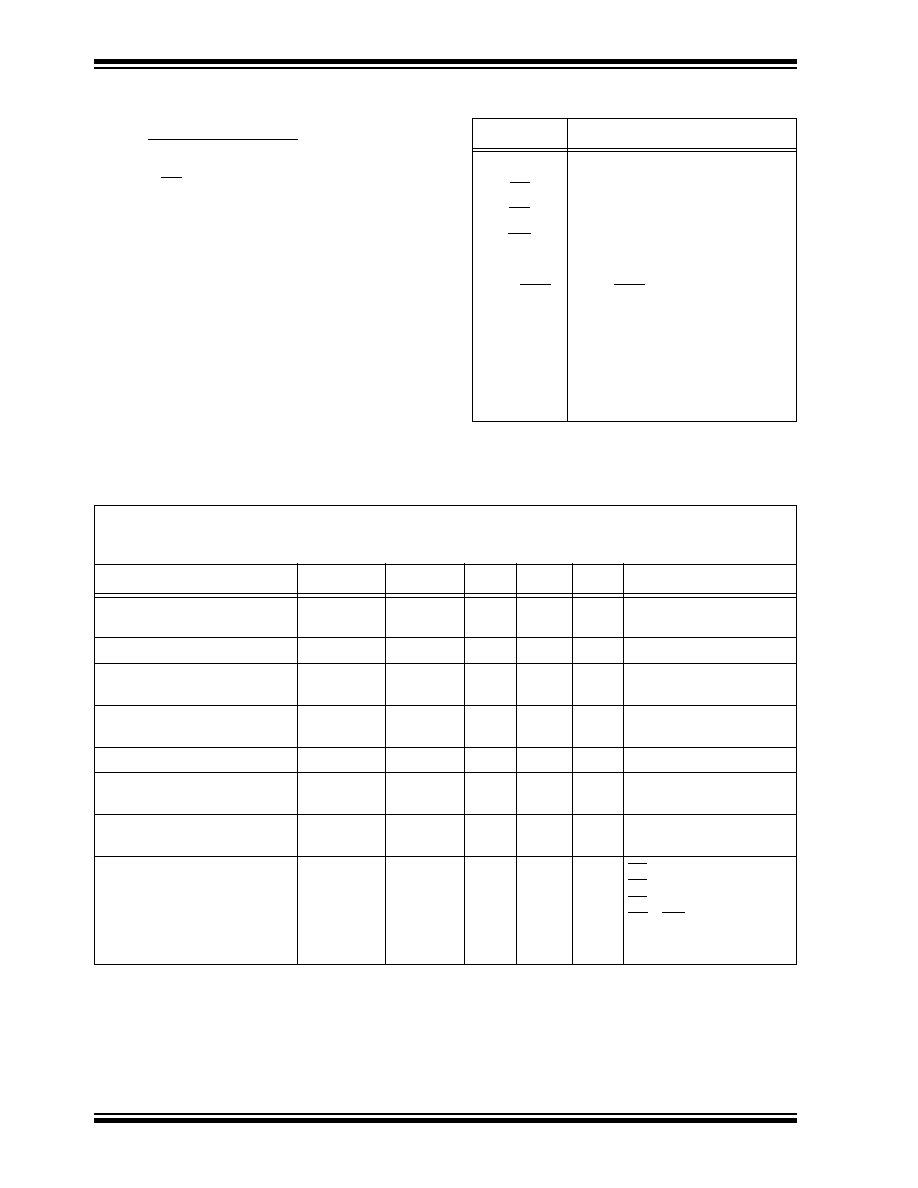
PACKAGE TYPES
BLOCK DIAGRAM
∑ Pin 1 indicator on PLCC on top of package
∑ 1
2
3
4
5
6
7
8
9
10
11
12
13
14
28
27
26
25
24
23
22
21
20
19
18
17
16
15
RDY/BSY
A12
A7
A6
A5
A4
A3
A2
A1
A0
I/O0
I/O1
I/O2
V
Vcc
WE
NC
A8
A9
A11
OE
A10
CE
I/O7
I/O6
I/O5
I/O4
I/O3
SS
A6
A5
A4
A3
A2
A1
A0
NC
I/O0
A8
A9
A11
NC
OE
A10
CE
I/O7
I/O6
A7
A12
RDY/BSY
NU
Vcc
WE
NC
I/O1
I/O2
Vss
NU
I/O3
I/O4
I/O5
14
15
16
17
18
19
20
4
3
2
1
32
31
30
29
28
27
26
25
24
23
22
21
5
6
7
8
9
10
11
12
13
DIP/SOIC
PLCC
I/O0
I/O7
Input/Output
Buffers
Chip Enable/
Output Enable
Control Logic
CE
OE
Data Protection
Circuitry
A12
Y Gating
16K bit
Cell Matrix
X
Decoder
Y
Decoder
A0
Data
Poll
Auto Erase/Write
Timing
V
CC
V
SS
WE
L
a
t
c
h
e
s
Program Voltage
Generation
Rdy/
Busy
28C64A
64K (8K x 8) CMOS EEPROM
28C64A
DS11109J-page 2
©
1998 Microchip Technology Inc.
1.0 ELECTRICAL CHARACTERISTICS
1.1 MAXIMUM RATINGS*
V
CC
and input voltages w.r.t. V
SS
....... -0.6V to + 6.25V
Voltage on OE w.r.t. V
SS
.....................
. -0.6V to +13.5V
Voltage on A9 w.r.t. V
SS
......................
. -0.6V to +13.5V
Output Voltage w.r.t. V
SS
.................
.-0.6V to V
CC
+0.6V
Storage temperature .........................
. -65∞C to +125∞C
Ambient temp. with power applied........ -50∞C to +95∞C
*Notice:
Stresses ab
ove those listed unde
r "Maxi mum Ratings"
may cause pe
r manent damage to the d
evice. This is a stress
r at-
ing only and functional oper ation of the device at those or any
other conditions above those indicated in the ope
r ation listings of
this specification is not implied. Exposure to maximum r ating con-
ditions for extended per iods may affect device reliabilit y.
TABLE 1-1: PIN FUNCTION TABLE
Name Function
A0 - A12 Address Inputs
CE
Chip Enable
OE
Output Enable
WE
Wr ite Enable
I/O0 - I/O7 Data Inputs/Outputs
RDY/Busy
Ready/Busy
V
CC
+5V Power Supply
V
SS
Ground
NC No Connect; No Inter nal Connection
NU Not Used; No Exter nal Connection is
All owed
TABLE 1-2: READ/WRITE OPERATION DC CHARACTERISTIC
V
CC
= +5V
±
10%
Commercial (C): Tamb = 0∞C to +70∞C
Industr ial (I): Tamb = -40∞C to +85∞C
Parameter Status Symbol Min Max Units Conditions
Input Voltages Logic `1'
Logic `0'
V
IH
V
IL
2.0
-0.1
Vcc+1
0.8
V
V
Input Leakage -- I
LI
-10 10
µ
A
V
IN
= -0.1V to Vcc +1
Input Capacitance -- C
IN
--
10
pF
V
IN
= 0V; Tamb = 25∞C;
f = 1 MHz (Note 2)
Output Voltages Logic `1'
Logic `0'
V
OH
V
OL
2.4
0.45
V
V
I
OH
= -400
µ
A
I
OL
= 2.1 mA
Output Leakage -- I
LO
-10 10
µ
A
V
OUT
= -0.1V to Vcc +0.1V
Output Capacitance -- C
OUT
--
12
pF
V
IN
= 0V; Tamb = 25∞C;
f = 1 MHz (Note 2)
Power Supply Current, Acti ve TTL input I
CC
-- 30 mA f = 5 MHz (Note 1)
V
CC
= 5.5V
Power Supply Current, Standby TTL input
TTL input
CMOS input
I
CC
(
S
)
TTL
I
CC
(
S
)
TTL
I
CC
(
S
)
CMOS
--
2
3
100
mA
mA
µ
A
CE = V
IH
(0∞C to +70∞C)
CE = V
IH
(-40∞C to +85∞C)
CE = V
CC
-0.3 to Vcc +1
OE = WE = Vcc
All other inputs equal V
CC
or V
SS
Note 1: AC power supply current above 5MHz: 2mA/MHz.
2: Not 100% tested.

©
1998 Microchip Technology Inc.
DS11109J-page 3
28C64A
TABLE 1-3:
READ OPERATION AC CHARACTERISTICS
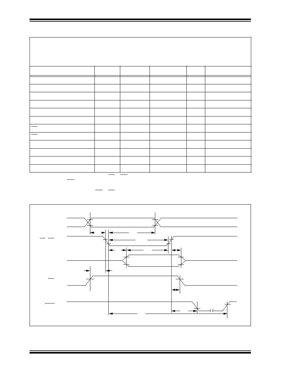
FIGURE 1-1:
READ WAVEFORMS
AC Testing Waveform:
V
IH
= 2.4V; V
IL
= 0.45V; V
OH
= 2.0V; V
OL
= 0.8V
Output Load:
1 TTL Load + 100 pF
Input Rise and Fall Times:
20 ns
Ambient Temperature:
Commercial (C):
Tamb
=
0∞C to +70∞C
Industrial (I):
Tamb
=
-40∞C to +85∞C
Parameter
Symbol
28C64A
-15
28C64A
-20
28C64A
-25
Units
Conditions
Min
Max
Min
Max
Min
Max
Address to Output Delay
t
ACC
--
150
--
200
--
250
ns
OE = CE = V
IL
CE to Output Delay
t
CE
--
150
--
200
--
250
ns
OE = V
IL
OE to Output Delay
t
OE
--
70
--
80
--
100
ns
CE = V
IL
CE or OE High to Output Float
t
OFF
0
50
0
55
0
70
ns
(Note 1)
Output Hold from Address, CE
or OE, whichever occurs first.
t
OH
0
--
0
--
0
--
ns
(Note 1)
Endurance
--
1M
--
1M
--
1M
--
cycles 25∞C, Vcc =
5.0V, Block
Mode (Note 2)
Note 1: Not 100% tested.
2: This parameter is not tested but guaranteed by characterization. For endurance estimates in a specific appli-
cation, please consult the Total Endurance Model which can be obtained on our BBS or website.
Address
CE
V
IH
V
IL
V
IH
V
IL
V
IH
V
IL
OE
Data
WE
V
OH
V
OL
V
IH
V
IL
Address Valid
High Z
Valid Output
t
ACC
(1) t
OFF
is specified for OE or CE, whichever occurs first
(2) OE may be delayed up to t
CE
- t
OE
after the falling edge of CE without impact on t
CE
(3) This parameter is sampled and is not 100% tested
High Z
t
OH
t
OFF(1,3)
Notes:
t
OE(2)
t
CE(2)
28C64A
DS11109J-page 4
©
1998 Microchip Technology Inc.
TABLE 1-4:
BYTE WRITE AC CHARACTERISTICS
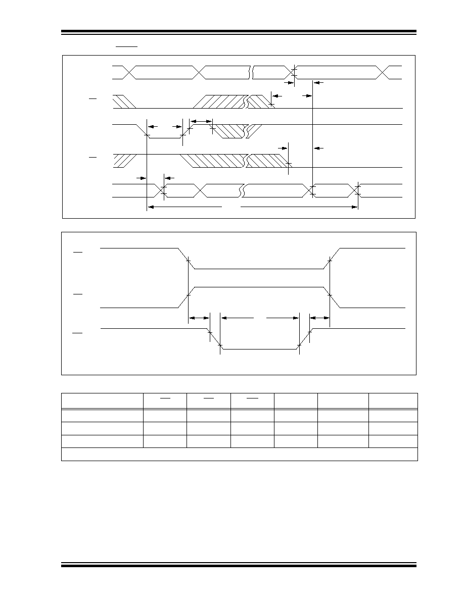
FIGURE 1-2:
PROGRAMMING WAVEFORMS
AC Testing Waveform:
V
IH
= 2.4V; V
IL
= 0.45V; V
OH
= 2.0V; V
OL
= 0.8V
Output Load:
1 TTL Load + 100 pF
Input Rise/Fall Times:
20 ns
Ambient Temperature:
Commercial (C):
Tamb
=
0∞C to +70∞C
Industrial (I):
Tamb
=
-40∞C to +85∞C
Parameter
Symbol
Min
Max
Units
Remarks
Address Set-Up Time
t
AS
10
--
ns
Address Hold Time
t
AH
50
--
ns
Data Set-Up Time
t
DS
50
--
ns
Data Hold Time
t
DH
10
--
ns
Write Pulse Width
t
WPL
100
--
ns
Note 1
Write Pulse High Time
t
WPH
50
--
ns
OE Hold Time
t
OEH
10
--
ns
OE Set-Up Time
t
OES
10
--
ns
Data Valid Time
t
DV
--
1000
ns
Note 2
Time to Device Busy
t
DB
2
50
ns
Write Cycle Time (
28C64A
)
t
WC
--
1
ms
0.5 ms typical
Write Cycle Time (
28C64A
F)
t
WC
--
200
µ
s
100
µ
s typical
Note 1: A write cycle can be initiated be CE or WE going low, whichever occurs last. The data is latched on the pos-
itive edge WE, whichever occurs first.
2: Data must be valid within 1000ns max. after a write cycle is initiated and must be stable at least until t
DH
after the positive edge of WE or CE, whichever occurs first.
t
AS
t
AH
t
WPL
t
DS
t
DH
t
OES
t
OEH
t
WC
Address
CE, WE
Data In
OE
V
IH
V
IL
V
IH
V
IL
V
IH
V
IL
V
IH
V
IL
Rdy/Busy
V
OH
V
OL
t
DB
t
DV
Busy
Ready
©
1998 Microchip Technology Inc.
DS11109J-page 5
28C64A
FIGURE 1-3:
DATA POLLING WAVEFORMS
FIGURE 1-4:
CHIP CLEAR WAVEFORMS
TABLE 1-5:
SUPPLEMENTARY CONTROL
Mode
CE
OE
WE
A9
V
CC
I/O
I
Chip Clear
V
IL
V
IH
V
IL
X
V
CC
Extra Row Read
V
IL
V
IL
V
IH
A9 = V
H
V
CC
Data Out
Extra Row Write
*
V
IH
*
A9 = V
H
V
CC
Data In
Note:
V
H
= 12.0V
±
0.5V. *Pulsed per programming waveforms.
Address Valid
Last Written
Address Valid
t
ACC
t
CE
t
WPL
t
WPH
t
DV
t
WC
t
OE
True Data Out
Data In
Valid
V
IH
V
IL
Data
OE
WE
CE
Address
I/O7 Out
V
IH
V
IL
V
IH
V
IL
V
IH
V
IL
V
IH
V
IL
V
H
V
IH
CE
OE
WE
t
S
t
H
t
W
t
S
= = 1
µ
s
t
H
= 10ms
t
W
V
IH
V
IL
V
IH
V
IL
= 12.0V
±
0.5V
V
H
28C64A
DS11109J-page 6
©
1998 Microchip Technology Inc.
2.0
DEVICE OPERATION
The Microchip Technology Inc.
28C64A
has four basic
modes of operation--read, standby, write inhibit, and
byte write--as outlined in the following table.
2.1
Read Mode
The
28C64A
has two control functions, both of which
must be logically satisfied in order to obtain data at the
outputs. Chip enable (CE) is the power control and
should be used for device selection. Output Enable
(OE) is the output control and is used to gate data to
the output pins independent of device selection.
Assuming that addresses are stable, address access
time (tACC) is equal to the delay from CE to output
(tCE). Data is available at the output t
OE
after the fall-
ing edge of OE, assuming that CE has been low and
addresses have been stable for at least t
ACC
-t
OE
.
2.2
Standby Mode
The
28C64A
is placed in the standby mode by applying
a high signal to the CE input. When in the standby
mode, the outputs are in a high impedance state, inde-
pendent of the OE input.
2.3
Data Protection
In order to ensure data integrity, especially during criti-
cal power-up and power-down transitions, the following
enhanced data protection circuits are incorporated:
First, an internal V
CC
detect (3.3 volts typical) will inhibit
the initiation of non-volatile programming operation
when V
CC
is less than the V
CC
detect circuit trip.
Second, there is a WE filtering circuit that prevents WE
pulses of less than 10 ns duration from initiating a write
cycle.
Third, holding WE or CE high or OE low, inhibits a write
cycle during power-on and power-off (V
CC
).
Operation
Mode
CE
OE
WE
I/O
Rdy/Busy
(1)
Read
L
L
H
D
OUT
H
Standby
H
X
X
High Z
H
Write Inhibit
H
X
X
High Z
H
Write Inhibit
X
L
X
High Z
H
Write Inhibit
X
X
H
High Z
H
Byte Write
L
H
L
D
IN
L
Byte Clear
Automatic Before Each "Write"
Note 1: Open drain output.
2: X = Any TTL level.
2.4
Write Mode
The
28C64A
has a write cycle similar to that of a Static
RAM. The write cycle is completely self-timed and ini-
tiated by a low going pulse on the WE pin. On the fall-
ing edge of WE, the address information is latched. On
rising edge, the data and the control pins (CE and OE)
are latched. The Ready/Busy pin goes to a logic low
level indicating that the
28C64A
is in a write cycle which
signals the microprocessor host that the system bus is
free for other activity. When Ready/Busy goes back to
a high, the
28C64A
has completed writing and is ready
to accept another cycle.
2.5
Data Polling
The
28C64A
features Data polling to signal the comple-
tion of a byte write cycle. During a write cycle, an
attempted read of the last byte written results in the
data complement of I/O7
(I/O0 to I/O6 are indetermin-
able). After completion of the write cycle, true data is
available. Data polling allows a simple read/compare
operation to determine the status of the chip eliminat-
ing the need for external hardware.
2.6
Electronic Signature for Device
Identification
An extra row of 32 bytes of EEPROM memory is avail-
able to the user for device identification. By raising A9
to 12V
±
0.5V and using address locations 1FEO to
1FFF, the additional bytes can be written to or read
from in the same manner as the regular memory array.
2.7
Chip Clear
All data may be cleared to 1's in a chip clear cycle by
raising OE to 12 volts and bringing the WE and CE low.
This procedure clears all data, except for the extra row.
28C64A
28C64A Product Identification System
To order or to obtain information, e.g., on pricing or delivery, please use the listed part numbers, and refer to the factory or the listed
sales offices.
Package:
L = Plastic Leaded Chip Carrier (PLCC)
P = Plastic DIP (600 mil)
SO = Plastic Small Outline IC (600 mil)
Temperature
Blank = 0
∞
C to +70
∞
C
Range:
I
= -40
∞
C to +85
∞
C
Access Time:
15
150 ns
20
200 ns
25
250 ns
Shipping:
Blank
Tube
T
Tape and Reel "L" and "SO"
Option:
Blank = twc = 1ms
F = twc = 200
µ
s
Device:
28C64A
8K x 8 CMOS EEPROM
28C64A
F
T
≠
15
I
/P
©
1998 Microchip Technology Inc.
DS11109J-page 7
2002 Microchip Technology Inc.
Information contained in this publication regarding device
applications and the like is intended through suggestion only
and may be superseded by updates. It is your responsibility to
ensure that your application meets with your specifications.
No representation or warranty is given and no liability is
assumed by Microchip Technology Incorporated with respect
to the accuracy or use of such information, or infringement of
patents or other intellectual property rights arising from such
use or otherwise. Use of Microchip's products as critical com-
ponents in life support systems is not authorized except with
express written approval by Microchip. No licenses are con-
veyed, implicitly or otherwise, under any intellectual property
rights.
Trademarks
The Microchip name and logo, the Microchip logo, FilterLab,
K
EE
L
OQ
, microID, MPLAB, PIC, PICmicro, PICMASTER,
PICSTART, PRO MATE, SEEVAL and The Embedded Control
Solutions Company are registered trademarks of Microchip Tech-
nology Incorporated in the U.S.A. and other countries.
dsPIC, ECONOMONITOR, FanSense, FlexROM, fuzzyLAB,
In-Circuit Serial Programming, ICSP, ICEPIC, microPort,
Migratable Memory, MPASM, MPLIB, MPLINK, MPSIM,
MXDEV, PICC, PICDEM, PICDEM.net, rfPIC, Select Mode
and Total Endurance are trademarks of Microchip Technology
Incorporated in the U.S.A.
Serialized Quick Turn Programming (SQTP) is a service mark
of Microchip Technology Incorporated in the U.S.A.
All other trademarks mentioned herein are property of their
respective companies.
© 2002, Microchip Technology Incorporated, Printed in the
U.S.A., All Rights Reserved.
Printed on recycled paper.
Microchip received QS-9000 quality system
certification for its worldwide headquarters,
design and wafer fabrication facilities in
Chandler and Tempe, Arizona in July 1999. The
Company's quality system processes and
procedures are QS-9000 compliant for its
PICmicro
Æ
8-bit MCUs, K
EE
L
OQ
Æ
code hopping
devices, Serial EEPROMs and microperipheral
products. In addition, Microchip's quality
system for the design and manufacture of
development systems is ISO 9001 certified.
Note the following details of the code protection feature on PICmicro
Æ
MCUs.
∑
The PICmicro family meets the specifications contained in the Microchip Data Sheet.
∑
Microchip believes that its family of PICmicro microcontrollers is one of the most secure products of its kind on the market today,
when used in the intended manner and under normal conditions.
∑
There are dishonest and possibly illegal methods used to breach the code protection feature. All of these methods, to our knowl-
edge, require using the PICmicro microcontroller in a manner outside the operating specifications contained in the data sheet.
The person doing so may be engaged in theft of intellectual property.
∑
Microchip is willing to work with the customer who is concerned about the integrity of their code.
∑
Neither Microchip nor any other semiconductor manufacturer can guarantee the security of their code. Code protection does not
mean that we are guaranteeing the product as "unbreakable".
∑
Code protection is constantly evolving. We at Microchip are committed to continuously improving the code protection features of
our product.
If you have any further questions about this matter, please contact the local sales office nearest to you.

2002 Microchip Technology Inc.
M
AMERICAS
Corporate Office
2355 West Chandler Blvd.
Chandler, AZ 85224-6199
Tel: 480-792-7200 Fax: 480-792-7277
Technical Support: 480-792-7627
Web Address: http://www.microchip.com
Rocky Mountain
2355 West Chandler Blvd.
Chandler, AZ 85224-6199
Tel: 480-792-7966 Fax: 480-792-7456
Atlanta
500 Sugar Mill Road, Suite 200B
Atlanta, GA 30350
Tel: 770-640-0034 Fax: 770-640-0307
Boston
2 Lan Drive, Suite 120
Westford, MA 01886
Tel: 978-692-3848 Fax: 978-692-3821
Chicago
333 Pierce Road, Suite 180
Itasca, IL 60143
Tel: 630-285-0071 Fax: 630-285-0075
Dallas
4570 Westgrove Drive, Suite 160
Addison, TX 75001
Tel: 972-818-7423 Fax: 972-818-2924
Detroit
Tri-Atria Office Building
32255 Northwestern Highway, Suite 190
Farmington Hills, MI 48334
Tel: 248-538-2250 Fax: 248-538-2260
Kokomo
2767 S. Albright Road
Kokomo, Indiana 46902
Tel: 765-864-8360 Fax: 765-864-8387
Los Angeles
18201 Von Karman, Suite 1090
Irvine, CA 92612
Tel: 949-263-1888 Fax: 949-263-1338
New York
150 Motor Parkway, Suite 202
Hauppauge, NY 11788
Tel: 631-273-5305 Fax: 631-273-5335
San Jose
Microchip Technology Inc.
2107 North First Street, Suite 590
San Jose, CA 95131
Tel: 408-436-7950 Fax: 408-436-7955
Toronto
6285 Northam Drive, Suite 108
Mississauga, Ontario L4V 1X5, Canada
Tel: 905-673-0699 Fax: 905-673-6509
ASIA/PACIFIC
Australia
Microchip Technology Australia Pty Ltd
Suite 22, 41 Rawson Street
Epping 2121, NSW
Australia
Tel: 61-2-9868-6733 Fax: 61-2-9868-6755
China - Beijing
Microchip Technology Consulting (Shanghai)
Co., Ltd., Beijing Liaison Office
Unit 915
Bei Hai Wan Tai Bldg.
No. 6 Chaoyangmen Beidajie
Beijing, 100027, No. China
Tel: 86-10-85282100 Fax: 86-10-85282104
China - Chengdu
Microchip Technology Consulting (Shanghai)
Co., Ltd., Chengdu Liaison Office
Rm. 2401, 24th Floor,
Ming Xing Financial Tower
No. 88 TIDU Street
Chengdu 610016, China
Tel: 86-28-6766200 Fax: 86-28-6766599
China - Fuzhou
Microchip Technology Consulting (Shanghai)
Co., Ltd., Fuzhou Liaison Office
Unit 28F, World Trade Plaza
No. 71 Wusi Road
Fuzhou 350001, China
Tel: 86-591-7503506 Fax: 86-591-7503521
China - Shanghai
Microchip Technology Consulting (Shanghai)
Co., Ltd.
Room 701, Bldg. B
Far East International Plaza
No. 317 Xian Xia Road
Shanghai, 200051
Tel: 86-21-6275-5700 Fax: 86-21-6275-5060
China - Shenzhen
Microchip Technology Consulting (Shanghai)
Co., Ltd., Shenzhen Liaison Office
Rm. 1315, 13/F, Shenzhen Kerry Centre,
Renminnan Lu
Shenzhen 518001, China
Tel: 86-755-2350361 Fax: 86-755-2366086
Hong Kong
Microchip Technology Hongkong Ltd.
Unit 901-6, Tower 2, Metroplaza
223 Hing Fong Road
Kwai Fong, N.T., Hong Kong
Tel: 852-2401-1200 Fax: 852-2401-3431
India
Microchip Technology Inc.
India Liaison Office
Divyasree Chambers
1 Floor, Wing A (A3/A4)
No. 11, O'Shaugnessey Road
Bangalore, 560 025, India
Tel: 91-80-2290061 Fax: 91-80-2290062
Japan
Microchip Technology Japan K.K.
Benex S-1 6F
3-18-20, Shinyokohama
Kohoku-Ku, Yokohama-shi
Kanagawa, 222-0033, Japan
Tel: 81-45-471- 6166 Fax: 81-45-471-6122
Korea
Microchip Technology Korea
168-1, Youngbo Bldg. 3 Floor
Samsung-Dong, Kangnam-Ku
Seoul, Korea 135-882
Tel: 82-2-554-7200 Fax: 82-2-558-5934
Singapore
Microchip Technology Singapore Pte Ltd.
200 Middle Road
#07-02 Prime Centre
Singapore, 188980
Tel: 65-334-8870 Fax: 65-334-8850
Taiwan
Microchip Technology Taiwan
11F-3, No. 207
Tung Hua North Road
Taipei, 105, Taiwan
Tel: 886-2-2717-7175 Fax: 886-2-2545-0139
EUROPE
Denmark
Microchip Technology Nordic ApS
Regus Business Centre
Lautrup hoj 1-3
Ballerup DK-2750 Denmark
Tel: 45 4420 9895 Fax: 45 4420 9910
France
Microchip Technology SARL
Parc d'Activite du Moulin de Massy
43 Rue du Saule Trapu
Batiment A - ler Etage
91300 Massy, France
Tel: 33-1-69-53-63-20 Fax: 33-1-69-30-90-79
Germany
Microchip Technology GmbH
Gustav-Heinemann Ring 125
D-81739 Munich, Germany
Tel: 49-89-627-144 0 Fax: 49-89-627-144-44
Italy
Microchip Technology SRL
Centro Direzionale Colleoni
Palazzo Taurus 1 V. Le Colleoni 1
20041 Agrate Brianza
Milan, Italy
Tel: 39-039-65791-1 Fax: 39-039-6899883
United Kingdom
Arizona Microchip Technology Ltd.
505 Eskdale Road
Winnersh Triangle
Wokingham
Berkshire, England RG41 5TU
Tel: 44 118 921 5869 Fax: 44-118 921-5820
01/18/02
W
ORLDWIDE
S
ALES
AND
S
ERVICE