©
1996 Microchip Technology Inc.
DS11109H-page 1
FEATURES
∑ Fast Read Access Time--150 ns
∑ CMOS Technology for Low Power Dissipation
- 30 mA Active
- 100
µ
A Standby
∑ Fast Byte Write Time--200
µ
s or 1 ms
∑ Data Retention >200 years
∑ High Endurance - Minimum 100,000
Erase/Write
Cycles
∑ Automatic Write Operation
- Internal Control Timer
- Auto-Clear Before Write Operation
- On-Chip Address and Data Latches
∑ Data Polling
∑ Ready/Busy
∑ Chip Clear Operation
∑ Enhanced Data Protection
- V
CC
Detector
- Pulse Filter
- Write Inhibit
∑ Electronic Signature for Device Identification
∑ 5-Volt-Only Operation
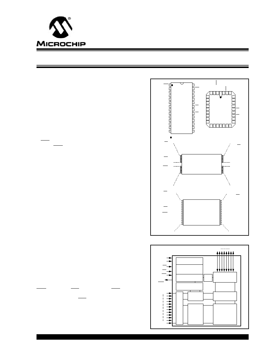
∑ Organized 8Kx8 JEDEC Standard Pinout
- 28-pin Dual-In-Line Package
- 32-pin PLCC Package
- 28-pin Thin Small Outline Package (TSOP)
8x20mm
- 28-pin Very Small Outline Package (VSOP)
8x13.4mm
∑ Available for Extended Temperature Ranges:
- Commercial: 0∞C to +70∞C
DESCRIPTION
The Microchip Technology Inc. 28C64A is a CMOS 64K non-
volatile electrically Erasable PROM. The 28C64A is
accessed like a static RAM for the read or write cycles without
the need of external components. During a "byte write", the
address and data are latched internally, freeing the micropro-
cessor address and data bus for other operations. Following
the initiation of write cycle, the device will go to a busy state
and automatically clear and write the latched data using an
internal control timer. To determine when the write cycle is
complete, the user has a choice of monitoring the Ready/
Busy output or using Data polling. The Ready/Busy pin is an
open drain output, which allows easy configuration in wired-
or systems. Alternatively, Data polling allows the user to read
the location last written to when the write operation is com-
plete. CMOS design and processing enables this part to be
used in systems where reduced power consumption and reli-
ability are required. A complete family of packages is offered
to provide the utmost flexibility in applications
PACKAGE TYPES
BLOCK DIAGRAM
A10
CE
21
20
19
V
SS
I/O2
14
13
12
OE
A11
A9
A8
22
23
24
RDY/BSY
A12
A7
1
2
3
4
5
25
26
27
28
6
7
NC
WE
V
CC
A6
A5
A4
A3
I/O7
I/O6
I/O5
I/O4
I/O3
I/O1
I/O0
A0
A1
A2
18
17
16
15
11
10
9
8
OE
A11
A9
A8
NC
WE
Vcc
RDY/BSY
A12
A7
A6
A5
A4
A3
A10
CE
I/07
I/06
I/05
I/04
I/03
Vss
I/02
I/01
I/00
A0
A1
A2
1
2
3
4
5
6
7
8
9
10
11
12
13
14
28
27
26
25
24
23
22
21
20
19
18
17
16
15
∑ Pin 1 indicator on PLCC on top of package
∑ 1
2
3
4
5
6
7
8
9
10
11
12
13
14
28
27
26
25
24
23
22
21
20
19
18
17
16
15
RDY/BSY
A12
A7
A6
A5
A4
A3
A2
A1
A0
I/O0
I/O1
I/O2
V
Vcc
WE
NC
A8
A9
A11
OE
A10
CE
I/O7
I/O6
I/O5
I/O4
I/O3
SS
A6
A5
A4
A3
A2
A1
A0
NC
I/O0
A8
A9
A11
NC
OE
A10
CE
I/O7
I/O6
A7
A12
RDY/BSY
NU
Vcc
WE
NC
I/O1
I/O2
Vss
NU
I/O3
I/O4
I/O5
14
15
16
17
18
19
20
4
3
2
1
32
31
30
29
28
27
26
25
24
23
22
21
5
6
7
8
9
10
11
12
13
DIP/SOIC
PLCC
TSOP
VSOP
I/O0
I/O7
Input/Output
Buffers
Chip Enable/
Output Enable
Control Logic
CE
OE
Data Protection
Circuitry
A12
Y Gating
16K bit
Cell Matrix
X
Decoder
Y
Decoder
A0
Data
Poll
Auto Erase/Write
Timing
V
CC
V
SS
WE
L
a
t
c
h
e
s
Program Voltage
Generation
Rdy/
Busy
28C64A
64K (8K x 8) CMOS EEPROM
This document was created with FrameMaker 4 0 4
28C64A
DS11109H-page 2
©
1996 Microchip Technology Inc.
1.0
ELECTRICAL CHARACTERISTICS
1.1
MAXIMUM RATINGS*
V
CC
and input voltages w.r.t. V
SS
....... -0.6V to + 6.25V
Voltage on OE w.r.t. V
SS
..................... -0.6V to +13.5V
Voltage on A9 w.r.t. V
SS
...................... -0.6V to +13.5V
Output Voltage w.r.t. V
SS
................ -0.6V to V
CC
+0.6V
Storage temperature .......................... -65∞C to +125∞C
Ambient temp. with power applied ....... -50∞C to +95∞C
*Notice:
Stresses above those listed under "Maximum Ratings"
may cause permanent damage to the device. This is a stress rat-
ing only and functional operation of the device at those or any
other conditions above those indicated in the operation listings of
this specification is not implied. Exposure to maximum rating con-
ditions for extended periods may affect device reliability.
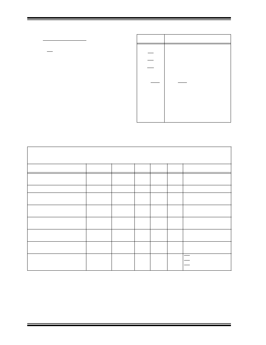
TABLE 1-1:
PIN FUNCTION TABLE
Name
Function
A0 - A12
Address Inputs
CE
Chip Enable
OE
Output Enable
WE
Write Enable
I/O0 - I/O7
Data Inputs/Outputs
RDY/Busy
Ready/Busy
V
CC
+5V Power Supply
V
SS
Ground
NC
No Connect; No Internal Connection
NU
Not Used; No External Connection is
Allowed
TABLE 1-2:
READ/WRITE OPERATION DC CHARACTERISTIC
V
CC
= +5V
±
10%
Commercial (C): Tamb = 0∞C to +70∞C
Industrial (I): Tamb = -40∞C to +85∞C
Parameter
Status
Symbol
Min
Max
Units
Conditions
Input Voltages
Logic `1'
Logic `0'
V
IH
V
IL
2.0
-0.1
Vcc+1
0.8
V
V
Input Leakage
--
I
LI
-10
10
µ
A
V
IN
= -0.1V to Vcc +1
Input Capacitance
--
C
IN
--
10
pF
V
IN
= 0V; Tamb = 25∞C;
f = 1 MHz (Note 2)
Output Voltages
Logic `1'
Logic `0'
V
OH
V
OL
2.4
0.45
V
V
I
OH
= -400
µ
A
I
OL
= 2.1 mA
Output Leakage
--
I
LO
-10
10
µ
A
V
OUT
= -0.1V to Vcc
+0.1V
Output Capacitance
--
C
OUT
--
12
pF
V
IN
= 0V; Tamb = 25∞C;
f = 1 MHz (Note 2)
Power Supply Current, Active
TTL input
I
CC
--
30
mA
f = 5 MHz (Note 1)
V
CC
= 5.5V
Power Supply Current, Standby
TTL input
TTL input
CMOS input
I
CC
(
S
)
TTL
I
CC
(
S
)
TTL
I
CC
(
S
)
CMOS
--
2
3
100
mA
mA
µ
A
CE = V
IH
(0∞C to +70∞C)
CE = V
IH
(-40∞C to +85∞C)
CE = V
CC
-0.3 to Vcc +1
Note 1: AC power supply current above 5MHz: 2mA/MHz.
2: Not 100% tested.
©
1996 Microchip Technology Inc.
DS11109H-page 3
28C64A
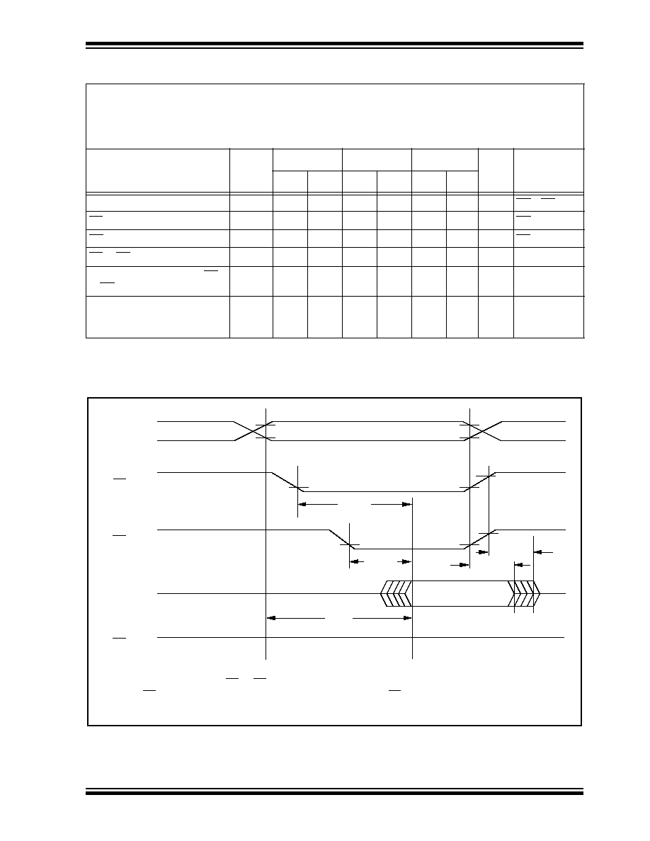
TABLE 1-3:
READ OPERATION AC CHARACTERISTICS
FIGURE 1-1:
READ WAVEFORMS
AC Testing Waveform:
V
IH
= 2.4V; V
IL
= 0.45V; V
OH
= 2.0V; V
OL
= 0.8V
Output Load:
1 TTL Load + 100 pF
Input Rise and Fall Times:
20 ns
Ambient Temperature:
Commercial (C):
Tamb
=
0∞C to +70∞C
Industrial (I):
Tamb
=
-40∞C to +85∞C
Parameter
Symbol
28C64A
-15
28C64A
-20
28C64A
-25
Units
Conditions
Min
Max
Min
Max
Min
Max
Address to Output Delay
t
ACC
--
150
--
200
--
250
ns
OE = CE = V
IL
CE to Output Delay
t
CE
--
150
--
200
--
250
ns
OE = V
IL
OE to Output Delay
t
OE
--
70
--
80
--
100
ns
CE = V
IL
CE or OE High to Output Float
t
OFF
0
50
0
55
0
70
ns
(Note 1)
Output Hold from Address, CE
or OE, whichever occurs first.
t
OH
0
--
0
--
0
--
ns
(Note 1)
Endurance
--
1M
--
1M
--
1M
--
cycles 25
∞
C, Vcc =
5.0V, Block
Mode (Note 2)
Note 1: Not 100% tested.
2: This parameter is not tested but guaranteed by characterization. For endurance estimates in a specific appli-
cation, please consult the Total Endurance Model which can be obtained on our BBS or website.
Address
CE
V
IH
V
IL
V
IH
V
IL
V
IH
V
IL
OE
Data
WE
V
OH
V
OL
V
IH
V
IL
Address Valid
High Z
Valid Output
t
ACC
(1) t
OFF
is specified for OE or CE, whichever occurs first
(2) OE may be delayed up to t
CE
- t
OE
after the falling edge of CE without impact on t
CE
(3) This parameter is sampled and is not 100% tested
High Z
t
OH
t
OFF(1,3)
Notes:
t
OE(2)
t
CE(2)

28C64A
DS11109H-page 4
©
1996 Microchip Technology Inc.
TABLE 1-4:
BYTE WRITE AC CHARACTERISTICS
FIGURE 1-2:
PROGRAMMING WAVEFORMS
AC Testing Waveform:
V
IH
= 2.4V; V
IL
= 0.45V; V
OH
= 2.0V; V
OL
= 0.8V
Output Load:
1 TTL Load + 100 pF
Input Rise/Fall Times:
20 ns
Ambient Temperature:
Commercial (C):
Tamb
=
0∞C to +70∞C
Industrial (I):
Tamb
=
-40∞C to +85∞C
Parameter
Symbol
Min
Max
Units
Remarks
Address Set-Up Time
t
AS
10
--
ns
Address Hold Time
t
AH
50
--
ns
Data Set-Up Time
t
DS
50
--
ns
Data Hold Time
t
DH
10
--
ns
Write Pulse Width
t
WPL
100
--
ns
Note 1
Write Pulse High Time
t
WPH
50
--
ns
OE Hold Time
t
OEH
10
--
ns
OE Set-Up Time
t
OES
10
--
ns
Data Valid Time
t
DV
--
1000
ns
Note 2
Time to Device Busy
t
DB
2
50
ns
Write Cycle Time (
28C64A
)
t
WC
--
1
ms
0.5 ms typical
Write Cycle Time (
28C64A
F)
t
WC
--
200
µ
s
100
µ
s typical
Note 1: A write cycle can be initiated be CE or WE going low, whichever occurs last. The data is latched on the pos-
itive edge WE, whichever occurs first.
2: Data must be valid within 1000ns max. after a write cycle is initiated and must be stable at least until t
DH
after
the positive edge of WE or CE, whichever occurs first.
t
AS
t
AH
t
WPL
t
DS
t
DH
t
OES
t
OEH
t
WC
Address
CE, WE
Data In
OE
V
IH
V
IL
V
IH
V
IL
V
IH
V
IL
V
IH
V
IL
Rdy/Busy
V
OH
V
OL
t
DB
t
DV
Busy
Ready

©
1996 Microchip Technology Inc.
DS11109H-page 5
28C64A
FIGURE 1-3:
DATA POLLING WAVEFORMS
FIGURE 1-4:
CHIP CLEAR WAVEFORMS
TABLE 1-5:
SUPPLEMENTARY CONTROL
Mode
CE
OE
WE
A9
V
CC
I/O
I
Chip Clear
V
IL
V
IH
V
IL
X
V
CC
Extra Row Read
V
IL
V
IL
V
IH
A9 = V
H
V
CC
Data Out
Extra Row Write
*
V
IH
*
A9 = V
H
V
CC
Data In
Note:
V
H
= 12.0V
±
0.5V. *Pulsed per programming waveforms.
Address Valid
Last Written
Address Valid
t
ACC
t
CE
t
WPL
t
WPH
t
DV
t
WC
t
OE
True Data Out
Data In
Valid
V
IH
V
IL
Data
OE
WE
CE
Address
I/O7 Out
V
IH
V
IL
V
IH
V
IL
V
IH
V
IL
V
IH
V
IL
V
H
V
IH
CE
OE
WE
t
S
t
H
t
W
t
S
= = 1
µ
s
t
H
= 10ms
t
W
V
IH
V
IL
V
IH
V
IL
= 12.0V
±
0.5V
V
H