©
1996 Microchip Technology Inc.
DS21109E-page 1
37LV36/65/128
FEATURES
∑ Operationally equivalent to Xilinx
Æ
XC1700 family
∑ Wide voltage range 3.0 V to 6.0 V
∑ Maximum read current 10 mA at 5.0 V
∑ Standby current 100
µ
A typical
∑ Industry standard Synchronous Serial Interface/
1 bit per rising edge of clock
∑ Full Static Operation
∑ Sequential Read/Program
∑ Cascadable Output Enable
∑ 10 MHz Maximum Clock Rate @ 5.0 Vdc
∑ Programmable Polarity on Hardware Reset
∑ Programming with industry standard EPROM pro-
grammers
∑ Electrostatic discharge protection > 4,000 volts
∑ 8-pin PDIP/SOIC and 20-pin PLCC packages
∑ Data Retention > 200 years
∑ Temperature ranges:
- Commercial: 0
∞
C to +70
∞
C
- Industrial: -40
∞
C to +85
∞
C
DESCRIPTION
The Microchip Technology Inc. 37LV36/65/128 is a
family of Serial OTP EPROM devices organized inter-
nally in a x32 configuration. The family also features a
cascadable option for increased memory storage
where needed. The 37LV36/65/128 is suitable for
many applications in which look-up table information
storage is desirable and provides full static operation in
the 3.0V to 6.0V V
CC
range. The devices also support
the industry standard serial interface to the popular
RAM-based Field Programmable Gate Arrays (FPGA).
Advanced CMOS technology makes this an ideal boot-
strap solution for today's high speed SRAM-based
FPGAs. The 37LV36/65/128 family is available in the
standard 8-pin plastic DIP, 8-pin SOIC and 20-pin
PLCC packages.
Device
Bits
Programming Word
37LV36
36,288
1134 x 32
37LV65
65,536
2048 x 32
37LV128
131,072
4096 x 32
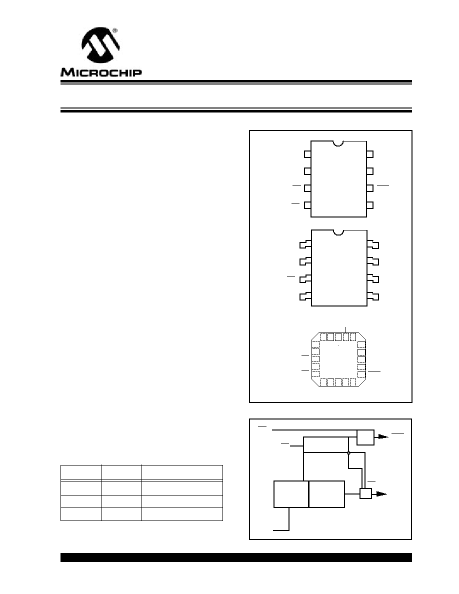
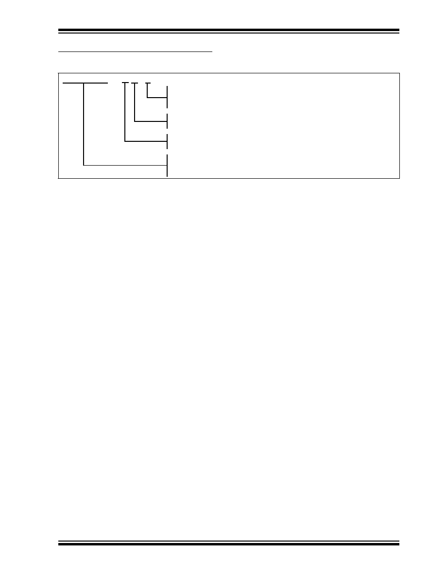
PACKAGE TYPES
BLOCK DIAGRAM
CLK
RESET/OE
CE
CEO
V
PP
Vss
9
10
11
12
13
3
2
1
20
19
18
17
16
15
14
4
5
6
7
8
V
CC
DATA
1
2
3
4
8
7
6
5
V
CC
V
PP
CEO
V
SS
DATA
CLK
RESET/OE
CE
1
2
3
4
8
7
6
5
DATA
CLK
RESET/OE
CE
V
CC
V
PP
CEO
V
SS
PDIP
37L
V36
37L
V65
37L
V128
SOIC
PLCC
37L
V36
37L
V65
37L
V128
37L
V36
37L
V65
37L
V128
OE
DATA
EPROM
ARRAY
CEO
ADDRESS
Counter
CLK
RESET/OE
CE
36K, 64K, and 128K Serial EPROM Family
Xilinx is a registered trademark of Xilinx Corporation.
This document was created with FrameMaker 4 0 4
37LV36/65/128
DS21109E-page 2
©
1996 Microchip Technology Inc.
1.0
ELECTRICAL CHARACTERISTICS
1.1
Maximum Ratings*
V
CC
and input voltages w.r.t. V
SS
.......... -0.6V to +0.6V
V
PP
voltage w.r.t. V
SS
during
programming ...................................... -0.6V to +14.0V
Output voltage w.r.t. V
SS
............... -0.6V to V
CC
+0.6V
Storage temperature .......................... -65∞C to +150∞C
Ambient temp. with power applied ..... -65∞C to +125∞C
Soldering temperature of leads (10 sec.) ......... +300
∞
C
ESD protection on all pins
.....................................
4 kV
*Notice: Stresses above those listed under "Maximum Ratings"
may cause permanent damage to the device. This is a stress rat-
ing only and functional operation of the device at those or any
other conditions above those indicated in the operation listings of
this specification is not implied. Exposure to maximum rating con-
ditions for extended periods may affect device reliability.
TABLE 1-1:
PIN FUNCTION TABLE
Name
Function
8
20
DATA
Data I/O
1
2
CLK
Clock Input
2
4
RESET/OE Reset Input and Output
Enable
3
6
CE
Chip Enable Input
4
8
V
SS
Ground
5
10
CEO
Chip Enable Output
6
14
V
PP
Programming Voltage Supply
7
17
V
CC
+3.0V to 6.0V Power Supply
8
20
Not Labeled Not utilized, not connected
TABLE 1-2:
READ OPERATION DC CHARACTERISTICS
V
CC
= +3.0 to 6.0V
Commercial (C):
Tamb = 0∞C to +70∞C
Industrial (I):
Tamb = -40∞C to +85∞C
Parameter
Symbol
Min.
Max.
Units
Conditions
DATA, CE, CEO and Reset pins:
High level input voltage
Low level input voltage
High level output voltage
Low level output voltage
V
IH
V
IL
V
OH1
V
OH2
V
OL
2.0
-0.3
3.86
2.4
--
V
CC
0.8
.32
V
V
V
V
I
OH
= -4 mA V
CC
4.5V
I
OH
= -4 mA V
CC
3.0V
I
OL
= 4.0 mA
Input Leakage
I
LI
-10
10
µ
A
V
IN
= .1V to V
CC
Output Leakage
I
LO
-10
10
µ
A
V
OUT
= .1V to V
CC
Input Capacitance
(all inputs/outputs)
C
INT
--
10
pF
Tamb = 25
∞
C; F
CLK
= 1 MHz (Note 1)
Operating Current
I
CC
Read
--
--
10
2
mA
mA
V
CC
= 6.0V, CLK = 10 MHz
V
CC
= 3.6V, CLK = 2.5 MHz
Outputs open
Standby Current
I
CCS
--
100
50
µ
A
µ
A
V
CC
= 6.0V, CE = 5.8V
V
CC
= 3.6V, CE = 3.4V
Note 1: This parameter is initially characterized and not 100% tested.

©
1996 Microchip Technology Inc.
DS21109E-page 3
37LV36/65/128
2.0
DATA
2.1
Data I/O
Three-state DATA output for reading and input during
programming.
3.0
CLK
3.1
Clock Input
Used to increment the internal address and bit
counters for reading and programming.
4.0
RESET/OE
4.1
Reset Input and Output Enable
A LOW level on both the CE and RESET/OE inputs
enables the data output driver. A HIGH level on
RESET/OE resets both the address and bit counters.
In the 37LVXXX, the logic polarity of this input is pro-
grammable as either RESET/OE or OE/RESET. This
document describes the pin as RESET/OE although
the opposite polarity is also possible. This option is
defined and set at device program time.
5.0
CE
5.1
Chip Enable Input
CE is used for device selection. A LOW level on both
CE and OE enables the data output driver. A HIGH
level on CE disables both the address and bit counters
and forces the device into a low power mode.
6.0
CEO
6.1
Chip Enable Output
This signal is asserted LOW on the clock cycle follow-
ing the last bit read from the memory. It will stay LOW
as long as CE and OE are both LOW. It will then follow
CE until OE goes HIGH. Thereafter, CEO will stay
HIGH until the entire EPROM is read again. This pin
also used to sense the status of RESET polarity when
Programming Mode is entered.
7.0
VPP
7.1
Programming Voltage Supply
Used to enter programming mode (+13 volts) and to
program the memory (+13 volts). Must be connected
directly to Vcc for normal Read operation. No over-
shoot above +14 volts is permitted.
8.0
CASCADING SERIAL EPROMS
Cascading Serial EPROMs provide additional memory
for multiple FPGAs configured as a daisy-chain, or for
future applications requiring larger configuration mem-
ories.
When the last bit from the first Serial EPROM is read,
the next clock signal to the Serial EPROM asserts its
CEO output LOW and disables its DATA line. The sec-
ond Serial EPROM recognizes the LOW level on its CE
input and enables its DATA output.
When configuration is complete, the address counters
of all cascaded Serial EPROMs are reset if RESET
goes LOW forcing the RESET/OE on each Serial
EPROM to go HIGH. If the address counters are not to
be reset upon completion, then the RESET/OE inputs
can be tied to ground.
Additional logic may be required if cascaded memories
are so large that the rippled chip enable is not fast
enough to activate successive Serial EPROMs.
9.0
STANDBY MODE
The 37LVXXX enters a low-power Standby Mode
whenever CE is HIGH. In Standby Mode, the Serial
EPROM consumes less than 100
µ
A of current. The
output will remain in a high-impedance state regardless
of the state of the OE input.
10.0
PROGRAMMING MODE
Programming Mode is entered by holding V
PP
HIGH
(+13 volts) for two clock edges and then holding V
PP
=
V
DD
for one clock edge. Programming mode is exited
by driving a LOW on both CE and OE and then remov-
ing power from the device. Figures 4 through 7 show
the programming algorithm.
11.0
37LVXXX RESET POLARITY
The 37LVXXX lets the user choose the reset polarity as
either RESET/OE or OE/RESET. Any third-party com-
mercial programmer should prompt the user for the
desired reset polarity.
The programming of the overflow word should be han-
dled transparently by the EPROM programmer; it is
mentioned here as supplemental information only.
The polarity is programmed into the first overflow word
location, maximum address+1. 00000000 in these
locations makes the reset active LOW, FFFFFFFF in
these locations makes the reset active HIGH. The
default condition is RESET active HIGH.
37LV36/65/128
DS21109E-page 4
©
1996 Microchip Technology Inc.
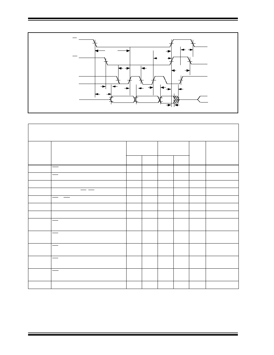
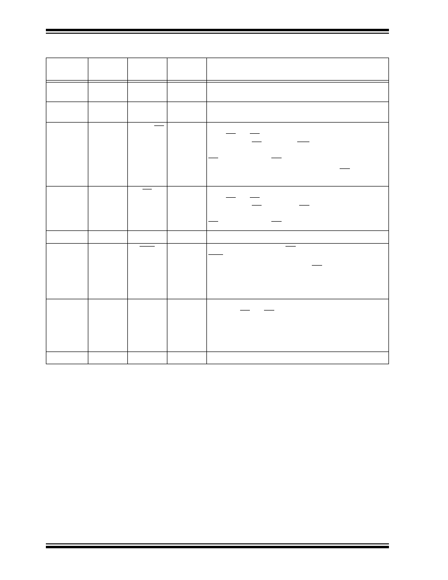
FIGURE 11-1: READ CHARACTERISTICS TIMING
TABLE 11-1:
READ CHARACTERISTICS
AC Testing Waveform: V
IL
= 0.2V; V
IH
= 3.0V
AC Test Load: 50 pF
V
OL
= V
OL
_MAX; V
OH
= V
OH
_MIN
Symbol
Parameter
Limits 3.0V
Vcc
6.0V
Limits 4.5V
Vcc
6.0V
Units
Conditions
Min.
Max.
Min.
Max.
T
OE
OE to Data Delay
--
45
--
45
ns
T
CE
CE to Data Delay
--
60
--
50
ns
T
CAC
CLK to Data Delay
--
200
--
60
ns
T
OH
Data Hold from CE, OE or CLK
0
--
0
--
ns
T
DF
CE or OE to Data Float Delay
--
50
--
50
ns
Notes 1, 2
T
LC
CLK Low Time
100
--
25
--
ns
T
HC
CLK High Time
100
--
25
--
ns
T
SCE
CE Set up Time to CLK
(to guarantee proper counting)
40
--
25
--
ns
Note 1
T
SCED
CE setup time to CLK
(to guarantee proper DATA read)
100
--
80
--
ns
T
HCE
CE Hold Time to CLK
(to guarantee proper counting)
0
--
0
--
ns
Note 1
T
HCED
CE hold time to CLK
(to guarantee proper DATA read)
50
--
0
--
ns
T
HOE
OE High Time
(Guarantees counters are Reset)
100
20
--
ns
CLK max
Clock Frequency
--
2.5
--
10
MHz
Note 1: This parameter is periodically sampled and not 100% tested.
2: Float delays are measured with output pulled through 1k
to V
LOAD
= V
CC
/2.
T
HCE
T
SCE
T
HOE
T
DF
T
OH
T
OH
T
HC
T
CAC
T
LC
T
SCE
T
OE
DATA
CLK
RESET/OE
CE
T
CE
T
SCED
T
HCED
©
1996 Microchip Technology Inc.
DS21109E-page 5
37LV36/65/128
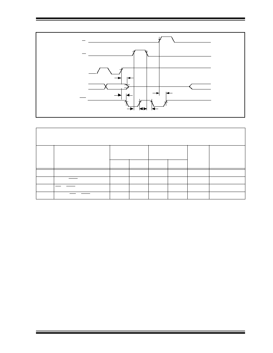
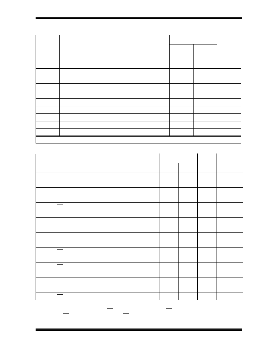
FIGURE 11-2: READ CHARACTERISTICS AT END OF ARRAY TIMING
TABLE 11-2:
READ CHARACTERISTICS AT END OF ARRAY
AC Testing Waveform: V
IL
= 0.2V; V
IH
= 3.0V
AC Test Load: 50 pF
V
OL
= V
OL
_MAX; V
OH
= V
OH
_MIN
Symbol
Parameter
Limits 3.0V
Vcc
6.0V
Limits 4.5V
Vcc
6.0V
Units
Conditions
Min.
Max.
Min.
Max.
T
CDF
CLK to Data Float Delay
--
50
--
50
ns
Notes 1, 2
T
OCK
CLK to CEO Delay
--
65
--
40
ns
T
OCE
CE to CEO Delay
--
45
--
40
ns
T
OOE
RESET/OE to CEO Delay
--
45
--
40
ns
Note 1: This parameter is periodically sampled and not 100% tested.
2: Float delays are measured with output pulled through 1k
to V
LOAD
= V
CC
/2.
RESET/OE
FIRST BIT
T
OOE
T
OCE
T
OCE
LAST BIT
T
OCK
T
CDF
CE
CLK
DATA
CEO
37LV36/65/128
DS21109E-page 6
©
1996 Microchip Technology Inc.
TABLE 11-3:
PIN ASSIGNMENTS IN THE PROGRAMMING MODE
DIP/SOIC
Pin
PLCC Pin
Name
I/O
Description
1
2
DATA
I/O
The rising edge of the clock shifts a data word in or out of the
EPROM one bit at a time.
2
4
CLK
I
Clock Input. Used to increment the internal address/word
counter for reading and programming operation.
3
6
RESET/OE
I
The rising edge of CLK shifts a data word into the EPROM
when CE and OE are HIGH; it shifts a data word out of the
EPROM when CE is LOW and OE is HIGH. The address/
word counter is incremented on the rising edge of CLK while
CE is held HIGH and OE is held LOW.
Note 1: Any modified polarity of the RESET/OE pin is
ignored in the programming mode.
4
8
CE
I
The rising edge of CLK shifts a data word into the EPROM
when CE and OE are HIGH; it shifts a data word out of the
EPROM when CE is LOW and OE is HIGH. The address/
word counter is incremented on the rising edge of CLK while
CE is held HIGH and OE is held LOW.
5
10
V
SS
Ground pin.
6
14
CEO
O
The polarity of the RESET/OE pin can be read by sensing the
CEO pin.
Note 1: The polarity of the RESET/OE pin is ignored while in
the Programming Mode. In final verification, this pin
must be monitored to go LOW one clock cycle after
the last data bit has been read.
7
17
V
PP
Programming Voltage Supply. Programming Mode is entered
by holding CE and OE HIGH and V
PP
at V
PP
1 for two rising
clock edges and then lowering V
PP
to V
PP
2 for one more ris-
ing clock edge. A word is programmed by strobing the device
with V
PP
for the duration TPGM. V
PP
must be tied to V
CC
for
normal read operation.
8
20
V
CC
+5 V power supply input.
©
1996 Microchip Technology Inc.
DS21109E-page 7
37LV36/65/128
TABLE 11-4:
DC PROGRAMMING SPECIFICATIONS
TABLE 11-5:
AC PROGRAMMING SPECIFICATIONS (SEE NOTE 2)
Symbol
Parameter Ambient Temperature: Tamb = 25
∞
C
±
5
∞
C
Limits
Units
Min.
Max.
V
CCP
Supply voltage during programming
5.0
6.0
V
V
IL
Low-level input voltage
0.0
0.5
V
V
IH
High-level input voltage
2.4
V
CC
V
V
OL
Low-level output voltage
--
0.4
V
V
OH
High-level output voltage
3.7
--
V
V
PP
1
Programming voltage*
12.5
13.5
V
V
PP
2
Programming Mode access voltage
V
CCP
V
CCP
+1
V
I
PPP
Supply current in Programming Mode
--
100
mA
I
L
Input or output leakage current
-10
10
µ
A
V
CCL
First pass Low-level supply voltage for final verification
2.8
3.0
V
V
CCH
Second pass High-level supply voltage for final verification
6.4
6.6
V
* No overshoot is permitted on this signal. VPP must not be allowed to exceed 14 volts.
Symbol
Parameter
Limits
Units
Conditions
Min.
Max.
T
RPP
10% to 90% Rise Time of V
PP
1
µ
s
Note 1
T
FPP
90% to 10% Fall Time of V
PP
1
µ
s
Note 1
T
PGM
V
PP
Programming Pulse Width
.50
1.05
ms
T
SVC
V
PP
Setup to CLK for Entering Programming Mode
100
ns
Note 1
T
SVCE
CE Setup to CLK for Entering Programming Mode
100
ns
Note 1
T
SVOE
OE Setup to CLK for Entering Programming Mode
100
ns
Note 1
T
HVC
V
PP
Hold from CLK for Entering Programming Mode
300
ns
Note 1
T
SDP
Data Setup to CLK for Programming
50
ns
T
HDP
Data Hold from CLK for Programming
0
ns
T
LCE
CE Low time to clear data latches
100
ns
T
SCC
CE Setup to CLK for Programming/Verifying
100
ns
T
SIC
OE Setup to CLK for Incrementing Address Counter
100
ns
T
HIC
OE Hold from CLK for Incrementing Address Counter
0
ns
T
HOV
OE Hold from V
PP
200
ns
Note 1
T
PCAC
CLK to Data Valid
400
ns
T
POH
Data Hold from CLK
0
ns
T
PCE
CE Low to Data Valid
250
ns
Note 1: This parameter is periodically sampled and not 100% tested.
Note 2: While in Programming Mode, CE should only be changed while OE is HIGH and has been HIGH for 200 ns,
and OE should only be changed while CE is HIGH and has been HIGH for 200 ns.
37LV36/65/128
DS21109E-page 8
©
1996 Microchip Technology Inc.
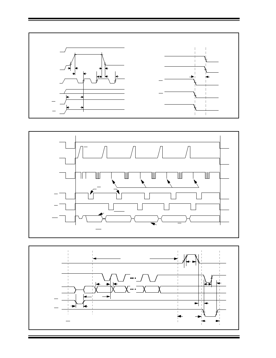
FIGURE 11-3: ENTER AND EXIT PROGRAMMING MODES
FIGURE 11-4: PROGRAMMING CYCLE OVERVIEW (NO VERIFY UNTIL ENTIRE ARRAY IS
PROGRAMMED)
FIGURE 11-5: DETAILS OF PROGRAM CYCLE
V
CC
V
PP
V
PP2
V
PP1
V
CCP
T
RPP
T
FPP
T
SVC
T
HVC
T
SVC
T
SVCE
T
SVOE
CLK
DATA
CE
RESET/OE
1
ms
V
SS
V
SS
V
SS
V
SS
V
SS
V
PP
V
CC
CE
RESET/OE
CLK
V
PP2
V
CCP
Enter Mode
Exit Mode
**
32 Clocks
*Note: The CEO pin is high impedance when V
PP
= V
PP
1
High if RESET/OE configured
Low if RESET/OE configured
2 CLKS
**Load
Word 1
**Load
Word 2
**Load
Word 3
**Load
Word 4
**Load
Word 5
CE low to clear
data latches
Clock Increments
Address Counter
Enter
Programming
Mode
500
µ
s
Programming
Mode
500
µ
s
Programming
Mode
500
µ
s
Programming
Mode
500
µ
s
Programming
Mode
V
PP
= V
PP2
V
CC
= V
CCP
V
PP1
V
CC
V
PP
CLK
CE
RESET/OE
CEO
*
*
*
*
*
V
PP
CLK
CE
RESET/OE
DATA
Load PROM
Internal
Data Latches
1
2
32 (Last Bit)
T
RPP
T
FPP
T
PGM
T
HOV
T
HDP
T
SCC
T
LCE
Clear PROM
Internal Data
Latches
Program
Pulse
Increment
Word
Counter
T
SDP
T
HIC
T
SIC
*Note: The programmer must float the data pin while
CE is low to avoid bus contention
*
©
1996 Microchip Technology Inc.
DS21109E-page 9
37LV36/65/128
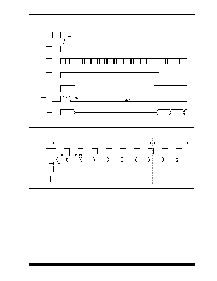
FIGURE 11-6: READ MANUFACTURER AND DEVICE ID OVERVIEW
FIGURE 11-7: DETAILS OF READ MANUFACTURER AND DEVICE ID
RESET/OE
V
CC
= V
CCP
V
CC
V
PP
CLK
CE
CEO
V
PP1
V
PP
= V
PP2
Enter
Programming
Mode
7 Clocks To
Read
Manufacturer ID
High if RESET/OE configured
Low if RESET/OE configured
Data
Clock past user memory array to ID location
(
)
37LV128 needs 4104 clocks
37LV36/65 needs 2056 clocks
8 Clocks To
Read Device ID
floats
LSB first
Microchip ID
Device ID
29 Hex
37LV128 = 72 Hex
37LV65 = 71 Hex
37LV36 = 70 Hex
X
DATA
RESET/OE
CE
CLK
T
PCE
LSB=1
0
0
1
0
1
0
0
LSB
∑ ∑ ∑
Device ID
Microchip ID = 29 Hex
T
PCAC
T
POH
∑ ∑ ∑

37LV36/65/128
DS21109E-page 10
©
1996 Microchip Technology Inc.
FIGURE 11-8: 37LVXXX PROGRAMMING SPECIFICATIONS
Device Passed
Device Failure
1st Pass?
Verify
All Data Bits (Read Mode)
V
CC
= V
PP
= V
CCL
and
V
CC
= V
PP
= V
CCH
Exit Programming Mode
Device Power Off
Device Power On
Pulse V
PP
to V
PP
1
(13V) for Tpgm
(500
µ
s)
Load 32-bit word to be
programmed
CE low to clear
EPROM internal data
latches
32 bit data word to be
programmed =
FFFFFFFFhex
Last Word?
Increment Address
Counter
Device Power Off
Device Power On
Check Device ID
Start
Enter Programming Mode
1.
V
CC
= V
CCP
V
PP
= V
PP
2 CE = OE = V
IH
2.
V
PP
= V
PP
1 for 2 CLK Rising Edges
3.
V
PP
= V
PP
2 for 1 CLK Rising Edge
Pass
No
Fail
Yes
No
Yes
No
Yes
37LV36/65/128
©
1996 Microchip Technology Inc.
DS21109E-page 11
37LV36/65/128 Product Identification System
To order or to obtain information, e.g., on pricing or delivery, please use the listed part numbers, and refer to the factory or the listed
sales offices.
Package:
P = Plastic DIP, 8 lead
SN = Plastic SOIC (150 mil Body), 8 lead
L = Plastic Leaded Chip Carrier (PLCC), 20 lead
Temperature
Blank = 0∞C to +70∞C
Range:
I
= -40∞C to +85∞C
Shipping:
Blank = Tube
T = Tape and Reel
Device:
37LV128
128K Serial EPROM
37LV65
64K Serial EPROM
37LV36
36K Serial EPROM
37LV36/65/128
≠
I
T
/P
DS21109E-page 12
©
1996 Microchip Technology Inc.
Information contained in this publication regarding device applications and the like is intended through suggestion only and may be superseded by updates. No repre-
sentation or warranty is given and no liability is assumed by Microchip Technology Incorporated with respect to the accuracy or use of such information, or infringement
of patents or other intellectual property rights arising from such use or otherwise. Use of Microchip's products as critical components in life support systems is not autho-
rized except with express written approval by Microchip. No licenses are conveyed, implicitly or otherwise, under any intellectual property rights. The Microchip logo and
name are registered trademarks of Microchip Technology Inc. All rights reserved. All other trademarks mentioned herein are the property of their respective companies.
W
ORLDWIDE
S
ALES
& S
ERVICE
ASIA/PACIFIC
China
Microchip Technology
Unit 406 of Shanghai Golden Bridge Bldg.
2077 Yan'an Road West, Hongiao District
Shanghai, Peoples Republic of China
Tel: 86 21 6275 5700
Fax: 011 86 21 6275 5060
Hong Kong
Microchip Technology
RM 3801B, Tower Two
Metroplaza
223 Hing Fong Road
Kwai Fong, N.T. Hong Kong
Tel: 852 2 401 1200 Fax: 852 2 401 3431
India
Microchip Technology
No. 6, Legacy, Convent Road
Bangalore 560 025 India
Tel: 91 80 526 3148 Fax: 91 80 559 9840
Korea
Microchip Technology
168-1, Youngbo Bldg. 3 Floor
Samsung-Dong, Kangnam-Ku,
Seoul, Korea
Tel: 82 2 554 7200 Fax: 82 2 558 5934
Singapore
Microchip Technology
200 Middle Road
#10-03 Prime Centre
Singapore 188980
Tel: 65 334 8870 Fax: 65 334 8850
Taiwan, R.O.C
Microchip Technology
10F-1C 207
Tung Hua North Road
Taipei, Taiwan, ROC
Tel: 886 2 717 7175 Fax: 886 2 545 0139
EUROPE
United Kingdom
Arizona Microchip Technology Ltd.
Unit 6, The Courtyard
Meadow Bank, Furlong Road
Bourne End, Buckinghamshire SL8 5AJ
Tel: 44 1628 850303 Fax: 44 1628 850178
France
Arizona Microchip Technology SARL
Zone Industrielle de la Bonde
2 Rue du Buisson aux Fraises
91300 Massy - France
Tel: 33 1 69 53 63 20 Fax: 33 1 69 30 90 79
Germany
Arizona Microchip Technology GmbH
Gustav-Heinemann-Ring 125
D-81739 Muenchen, Germany
Tel: 49 89 627 144 0 Fax: 49 89 627 144 44
Italy
Arizona Microchip Technology SRL
Centro Direzionale Colleone Pas Taurus 1
Viale Colleoni 1
20041 Agrate Brianza
Milan Italy
Tel: 39 39 6899939 Fax: 39 39 689 9883
JAPAN
Microchip Technology Intl. Inc.
Benex S-1 6F
3-18-20, Shin Yokohama
Kohoku-Ku, Yokohama
Kanagawa 222 Japan
Tel: 81 45 471 6166 Fax: 81 45 471 6122
9/3/96
AMERICAS
Corporate Office
Microchip Technology Inc.
2355 West Chandler Blvd.
Chandler, AZ 85224-6199
Tel: 602 786-7200 Fax: 602 786-7277
Technical Support: 602 786-7627
Web: http://www.microchip.com
Atlanta
Microchip Technology Inc.
500 Sugar Mill Road, Suite 200B
Atlanta, GA 30350
Tel: 770 640-0034 Fax: 770 640-0307
Boston
Microchip Technology Inc.
5 Mount Royal Avenue
Marlborough, MA 01752
Tel: 508 480-9990 Fax: 508 480-8575
Chicago
Microchip Technology Inc.
333 Pierce Road, Suite 180
Itasca, IL 60143
Tel: 708 285-0071 Fax: 708 285-0075
Dallas
Microchip Technology Inc.
14651 Dallas Parkway, Suite 816
Dallas, TX 75240-8809
Tel: 972 991-7177 Fax: 972 991-8588
Dayton
Microchip Technology Inc.
Suite 150
Two Prestige Place
Miamisburg, OH 45342
Tel: 513 291-1654 Fax: 513 291-9175
Los Angeles
Microchip Technology Inc.
18201 Von Karman, Suite 1090
Irvine, CA 92612
Tel: 714 263-1888 Fax: 714 263-1338
New York
Microchip Technmgy Inc.
150 Motor Parkway, Suite 416
Hauppauge, NY 11788
Tel: 516 273-5305 Fax: 516 273-5335
San Jose
Microchip Technology Inc.
2107 North First Street, Suite 590
San Jose, CA 95131
Tel: 408 436-7950 Fax: 408 436-7955
Toronto
Microchip Technology Inc.
5925 Airport Road, Suite 200
Mississauga, Ontario L4V 1W1, Canada
Tel: 905 405-6279
Fax: 905 405-6253
All rights reserved.
©
1996, Microchip Technology Incorporated, USA. 9/96
Printed on recycled paper.