 | –≠–ª–µ–∫—Ç—Ä–æ–Ω–Ω—ã–π –∫–æ–º–ø–æ–Ω–µ–Ω—Ç: HCS101 | –°–∫–∞—á–∞—Ç—å:  PDF PDF  ZIP ZIP |
©
2001 Microchip Technology Inc.
Preliminary
DS41115C-page 1
HCS101
FEATURES
Operating
∑ 2 Programmable 32-bit serial numbers
∑ 10-bit serial number
∑ 66-bit transmission code length
∑ Non-volatile 16-bit counter
∑ 3.5V -13.3V operation
∑ 3 inputs, 7 functions available
∑ Selectable baud rate
∑ Automatic code word completion
∑ Battery low signal transmitted to receiver
Other
∑ Pin-out compatible with most K
EE
L
OQ
Æ
Encoders
∑ Simple programming interface
∑ On-chip EEPROM
∑ On-chip oscillator and timing components
∑ Button inputs have internal pull-down resistors
∑ Minimum External Components required
Typical Applications
The HCS101 is ideal for remote control applications.
These applications include:
∑ Low-end automotive alarm systems
∑ Low-end automotive immobilizers
∑ Gate and garage door openers
∑ Identity tokens
∑ Low-end burglar alarm systems
∑ Fan and lighting controls
∑ Toys
DESCRIPTION
The HCS101 from Microchip Technology Inc. is a fixed
code encoder designed for remote control systems. It
provides a small package outline and low cost to make
this device a perfect solution for unidirectional remote
control systems.
It is also pin compatible with Microchip's HCS201 Code
Hopping Encoder allowing easy upgrading to a more
secure remote keyless entry (RKE) system.
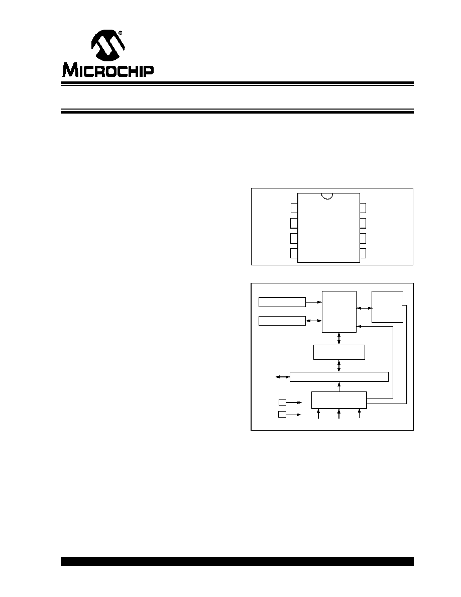
The 8-pin HCS101 operates over a wide voltage range
of 3.5V to 13.3V and has three button inputs allowing
the system designer the freedom to utilize up to 7 func-
tions. The only components required for device opera-
tion are the buttons and RF circuitry, allowing a very low
system cost.
PACKAGE TYPES
HCS101 BLOCK DIAGRAM
1
2
3
4
8
7
6
5
S0
S1
S2
NC
V
DD
NC
DATA
V
SS
PDIP, SOIC
HCS101
V
SS
V
DD
Power
latching
and
switching
Button input port
Transmit register
EEPROM
DATA
S2
S1
S0
Oscillator
RESET Circuit
Controller
Fixed Code Encoder
HCS101
DS41115C-page 2
Preliminary
©
2001 Microchip Technology Inc.
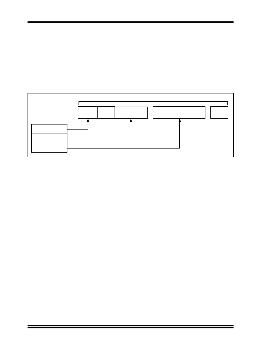
1.0
SYSTEM OVERVIEW
As indicated in the block diagram in Figure 1-1, the
HCS101 has a small EEPROM array, which must be
loaded with several parameters before use. These
parameters include:
∑ Two 32-bit serial numbers
∑ 16-bit counter value
∑ Additional 10-bit serial number
∑ Configuration data
The EEPROM data for each transmitter is programmed
by the manufacturer at the time of production.
Any type of controller may be used as a receiver, but it
is typically a microcontroller with compatible firmware
that allows the receiver to operate in conjunction with a
transmitter, based on the HCS101.
FIGURE 1-1:
BASIC OPERATION OF TRANSMITTER ENCODER
EEPROM Array
Serial Number 1
Transmitted Information
Serial Number 3
Counter
Counter
Serial
Number 3
Function
Bits
Function
Bits
Serial Number 1
©
2001 Microchip Technology Inc.
Preliminary
DS41115C-page 3
HCS101
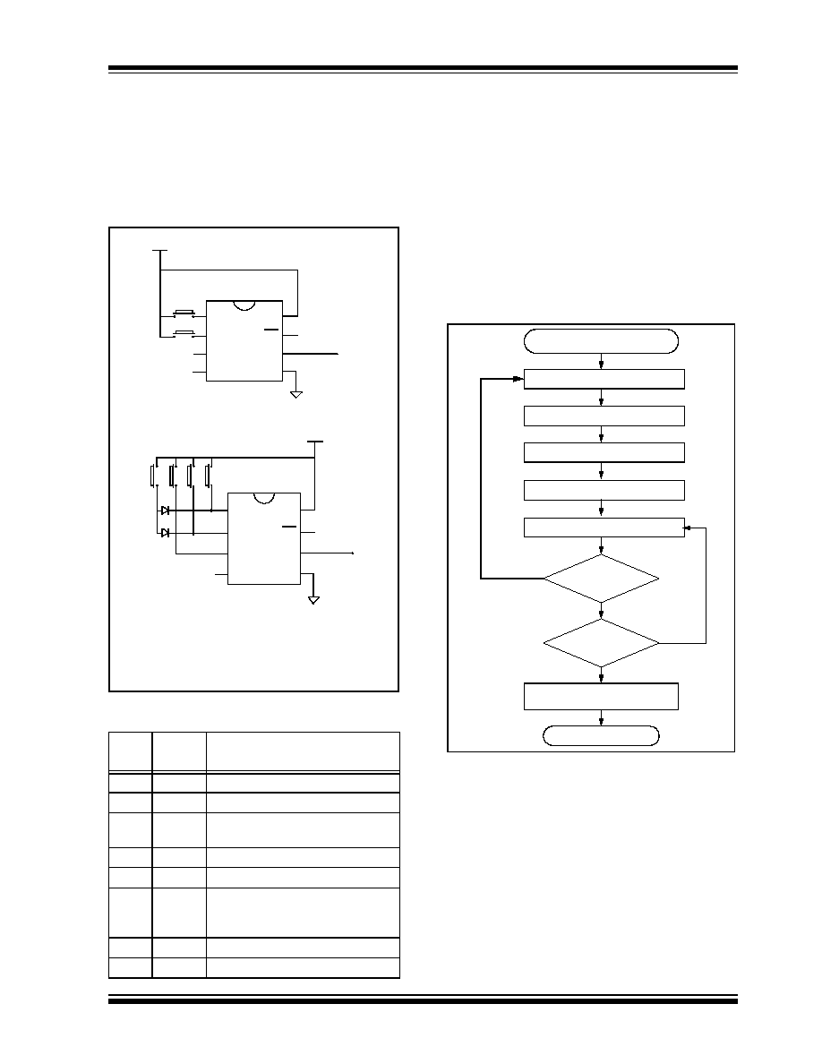
2.0
DEVICE OPERATION
As shown in the typical application circuits in Figure 2-
1, the HCS101 is easy to use. It requires only the addi-
tion of buttons and RF circuitry for use as the transmit-
ter in your application. A description of each pin is given
in Table 2-1.
FIGURE 2-1:
TYPICAL CIRCUITS
TABLE 2-1:
PIN DESCRIPTIONS
The HCS101 will wake-up upon detecting a switch clo-
sure and then delay for a debounce delay (T
DB
) as
shown in Figure 2-2. The device will then update the
16-bit counter before it loads the transmit register. The
data is then transmitted serially on the DATA pin in
Pulse Width Modulation (PWM) format.
If additional buttons are pressed during a transmission,
the current transmission is terminated. The HCS101
restarts and the new transmission will contain the latest
button information. When all buttons are released, the
device completes the current code word and then pow-
ers down. Released buttons do not terminate and/or
restart transmissions.
FIGURE 2-2:
ENCODER OPERATION
Name
Pin
Number
Description
S0
1
Switch input 0
S1
2
Switch input 1
S2
3
Switch input 2/Clock pin for
Programming mode
NC
4
No connection
V
SS
5
Ground reference connection
DATA
6
Pulse Width Modulation (PWM)
output pin/Data pin for
Programming mode
NC
7
No connection
V
DD
8
Positive supply voltage connection
V
DD
B0
Tx out
S0
S1
S2
NC
NC
V
DD
DATA
V
SS
2 button remote control
B1
Tx out
S0
S1
S2
NC
V
DD
DATA
V
SS
4 button remote control
B3 B2 B1 B0
Note:
Up to 7 functions can be implemented
by pressing more than one button
simultaneously or by using a suitable
diode array.
NC
V
DD
Power-Up
RESET and Debounce Delay
Sample Inputs
Update Counter
Load Transmit Register
Buttons
Added
?
All
Buttons
Released
?
(A button has been pressed)
Transmit
Stop
No
Yes
No
Yes
Complete Code
Word Transmission
HCS101
DS41115C-page 4
Preliminary
©
2001 Microchip Technology Inc.
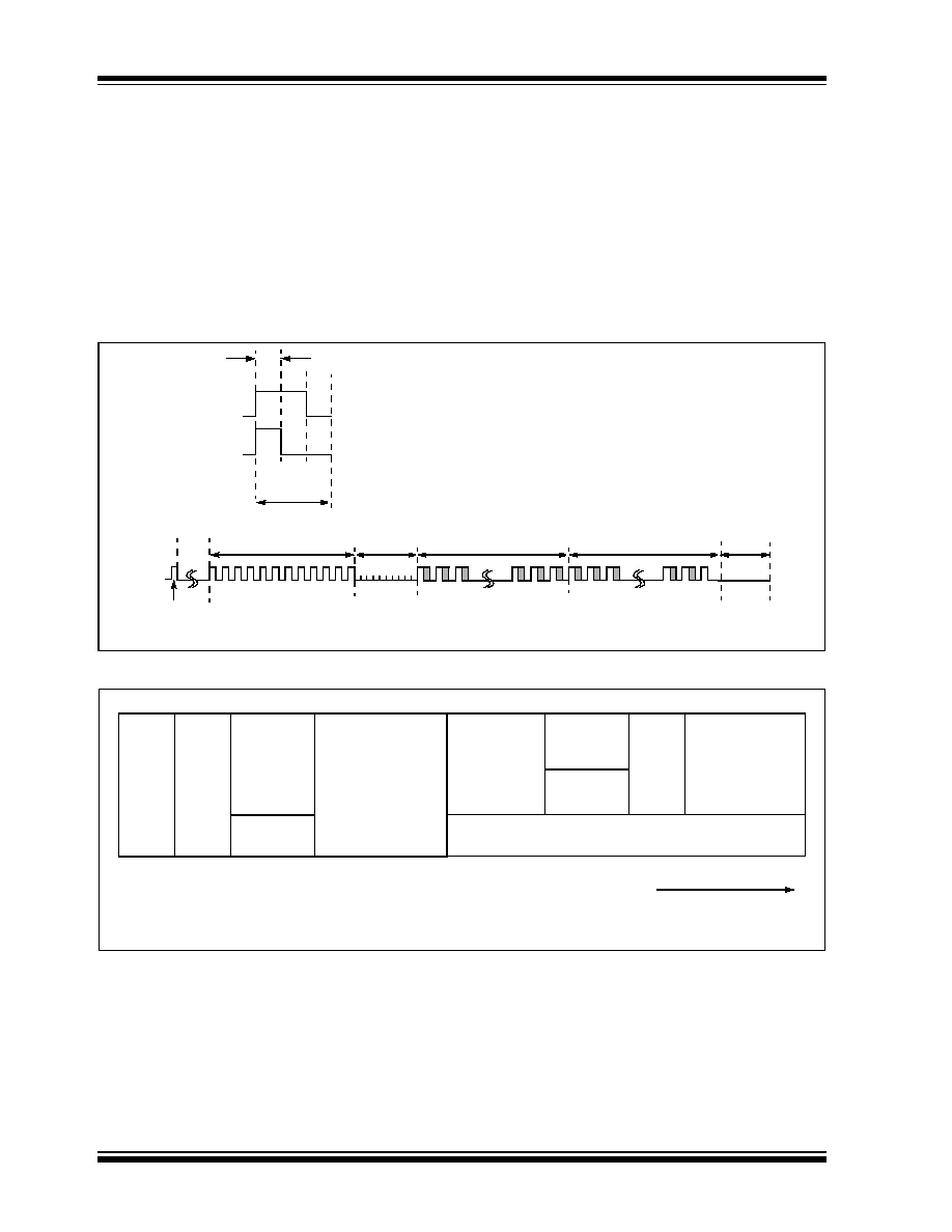
3.0
TRANSMITTED WORD
3.1
Transmission Format (PWM Mode)
The HCS101 transmission is made up of several code
words as shown in Figure 3-1. Each code word starts
with a preamble and a header, followed by the data.
The code word is followed by a guard period before the
next code word begins. The same code word is trans-
mitted as long as the button is pressed. Refer to
Table 7-3 for transmission timing requirements.
3.2
Code Word Organization
The HCS101 transmits a 66-bit code word. The 66-bit
word is constructed from the serial numbers, counter
and function information. The code word format is
shown in Figure 3-2.
Under normal conditions, serial number 1 is transmitted
with the counter and serial number 3. If all the buttons
are pressed, serial number 2 is transmitted in place of
the counter and serial number 3.
FIGURE 3-1:
CODE WORD TRANSMISSION FORMAT
FIGURE 3-2:
CODE WORD ORGANIZATION
LOGIC `0'
LOGIC `1'
Bit
Period
Preamble
Header
Counter, SER_3
and Function
Guard
Time
Tp
Th
Tg
Start Pulse
(Te)
SER_1
and Function
T
E
Serial Number 3
(10 bits)
Transmission Direction
Serial Number 1
Function**
(0/4 bits)
(32/28 bits)**
* See Section 4.3.6, S3 Setting (S3SET)
** See Section 4.3.7 Extended Serial Number (XSER)
*** Serial Number 2 is transmitted when all buttons are pressed
LSb first
S2 S1 S0 S3*
S2 S1 S0 S3*
(16 bits)
Counter
`00'
(2 bits)
Function
(4 bits)
`1'
(1 bit)
V
LOW
(1 bit)
Serial Number 2***
(32 bits)
MSb
LSb

©
2001 Microchip Technology Inc.
Preliminary
DS41115C-page 5
HCS101
4.0
EEPROM MEMORY
ORGANIZATION
The HCS101 contains 192 bits (12 x 16-bit words) of
EEPROM memory as shown in Table 4-1. Further
descriptions of the memory array are given in the fol-
lowing sections.
TABLE 4-1:
EEPROM MEMORY MAP
4.1
CNTR (Counter)
This is the 16-bit gray code counter value that can be
used to track the number of times a transmitter has
been activated.
4.2
SER_1, SER_2, SER_3 (Encoder
Serial Number)
SER_1, and SER_2 are the 32-bit device serial num-
bers. SER_3 is an additional 10-bit serial number trans-
mitted with every transmission. The most significant 6
bits of the 16-bit SER_3 word are reserved and should
be set to zero.
4.3
Configuration Word
The configuration word is a 16-bit word stored in the
EEPROM array that is used by the device to store the
status configuration options. Further explanations of
each of the bits are described in the following sections.
TABLE 4-2:
CONFIGURATION WORD
4.3.1
OSCILLATOR TUNING BITS
(OSC0 TO OSC3)
These bits are used to tune the nominal frequency of
the HCS101 to within ±10% of its nominal value over
temperature and voltage.
4.3.2
LOW VOLTAGE TRIP POINT
SELECT (V
LOWS
)
The low voltage trip point select bit (V
LOWS
) and the S3
setting bit (S3SET) are used to determine the voltage
level for the low voltage detector.
* See also Section 4.3.6
4.3.3
BAUDRATE SELECT BITS (BRS)
BRS selects the speed of transmission and the code
word blanking. Table 4-3 shows how the bit is used to
select the different baud rates and Section 5.2 provides
a detailed explanation of code word blanking.
TABLE 4-3:
BAUDRATE SELECT
WORD
ADDRESS
MNEMONIC
DESCRIPTION
0
RESERVED
Set to 0000H
1
RESERVED
Set to 0000H
2
RESERVED
Set to 0000H
3
RESERVED
Set to 0000H
4
CNTR
Counter
5
RESERVED
Set to 0000H
6
SER_1
Device Serial Number 1
(word 0) 16 LSb's
7
SER_1
Device Serial Number 1
(word 1) 16 MSb's
8
SER_2
Device Serial Number 2
(word 0) 16 LSb's
9
SER_2
Device Serial Number 2
(word 1) 16 MSb's
10
SER_3
Device Serial Number 3
11
CONFIG
Config Word
Bit Number
Bit Name
0
OSC0
1
OSC1
2
OSC2
3
OSC3
4
V
LOWS
5
BRS
6
MTX4
7
TXEN
8
S3SET
9
XSER
10
RESERVED
11
RESERVED
12
RESERVED
13
RESERVED
14
RESERVED
15
RESERVED
V
LOWS
S3SET*
Trip Point
0
0
4.4
0
1
4.4
1
0
9
1
1
6.75
BRS
Basic Pulse
Element
Code Words
Transmitted
0
400µs
All
1
200µs
1 out of 2