 | –≠–ª–µ–∫—Ç—Ä–æ–Ω–Ω—ã–π –∫–æ–º–ø–æ–Ω–µ–Ω—Ç: HCS361-IP | –°–∫–∞—á–∞—Ç—å:  PDF PDF  ZIP ZIP |
©
1996 Microchip Technology Inc.
Preliminary
DS40146C-page 1
M
FEATURES
Security
∑ Programmable 28/32-bit serial number
∑ Programmable 64-bit encryption key
∑ Each transmission is unique
∑ 67-bit transmission code length
∑ 32-bit hopping code
∑ 35-bit fixed code (28/32-bit serial number,
4/0-bit function code, 1-bit status, 2-bit CRC)
∑ Encryption keys are read protected
Operating
∑ 2.0-6.6V operation
∑ Four button inputs
- 15 functions available
∑ Selectable baud rate
∑ Automatic code word completion
∑ Battery low signal transmitted to receiver
∑ Nonvolatile synchronization data
∑ PWM and VPWM modulation
Other
∑ Easy to use programming interface
∑ On-chip EEPROM
∑ On-chip oscillator and timing components
∑ Button inputs have internal pulldown resistors
∑ Current limiting on LED output
∑ Minimum component count
Enhanced Features Over HCS300
∑ 48-bit seed vs. 32-bit seed
∑ 2-bit CRC for error detection
∑ 28/32-bit serial number select
∑ Two seed transmission methods
∑ PWM and VPWM modulation
∑ Wake-up signal in VPWM mode
∑ IR modulation mode
Typical Applications
The HCS361 is ideal for Remote Keyless Entry (RKE)
applications. These applications include:
∑ Automotive RKE systems
∑ Automotive alarm systems
∑ Automotive immobilizers
∑ Gate and garage door openers
∑ Identity tokens
∑ Burglar alarm systems
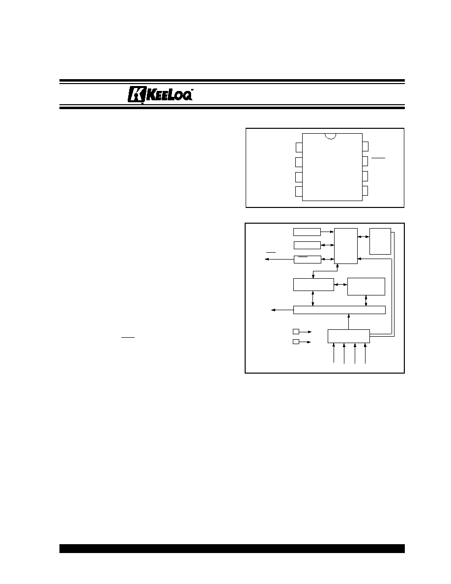
PACKAGE TYPES
HCS361 BLOCK DIAGRAM
DESCRIPTION
The HCS361 is a code hopping encoder designed for
secure Remote Keyless Entry (RKE) systems. The
HCS361 utilizes the K
EE
L
OQ
code hopping technology,
which incorporates high security, a small package
outline and low cost, to make this device a perfect
solution for unidirectional remote keyless entry systems
and access control systems.
The HCS361 combines a 32-bit hopping code
generated by a nonlinear encryption algorithm, with a
28/32-bit serial number and 7/3 status bits to create a
67-bit transmission stream. The length of the
transmission eliminates the threat of code scanning
and the code hopping mechanism makes each
transmission unique, thus rendering code capture and
resend (code grabbing) schemes useless.
1
2
3
4
8
7
6
5
S0
S1
S2
S3
V
DD
LED
PWM
V
SS
PDIP, SOIC
HCS361
V
SS
V
DD
Oscillator
Reset circuit
LED driver
Controller
Power
latching
and
switching
Button input port
32-bit shift register
Encoder
EEPROM
PWM
LED
S
3
S
2
S
1
S
0
K
EE
L
OQ
is a trademark of Microchip Technology Inc.
*Code hopping encoder patents issued in Europe, U. S. A., R. S. A. -- US: 5,517,187; Europe: 0459781
HCS361
Code Hopping Encoder*

HCS361
DS40146C-page 2
Preliminary
©
1996 Microchip Technology Inc.
The encryption key, serial number, and configuration
data are stored in EEPROM which is not accessible via
any external connection. This makes the HCS361 a
very secure unit. The HCS361 provides an easy to use
serial interface for programming the necessary security
keys, system parameters, and configuration data.
The encryption keys and code combinations are pro-
grammable but read-protected. The keys can only be
verified after an automatic erase and programming
operation. This protects against attempts to gain
access to keys and manipulate synchronization values.
The HCS361 operates over a wide voltage range of
2.0V to 6.6V and has four button inputs in an 8-pin
configuration. This allows the system designer the
freedom to utilize up to 15 functions. The only
components required for device operation are the but-
tons and RF circuitry, allowing a very low system cost.
1.0
SYSTEM OVERVIEW
1.1
Key Terms
∑ Manufacturer's Code ≠ a 64-bit word, unique to
each manufacturer, used to produce a unique
encryption key in each transmitter (encoder).
∑ Encryption Key ≠ a unique 64-bit key generated
and programmed into the encoder during the
manufacturing process. The encryption key
controls the encryption algorithm and is stored in
EEPROM on the encoder device.
∑ Learn ≠ The HCS product family facilitates several
learning strategies to be implemented on the
decoder. The following are examples of what can
be done.
Normal Learning
The receiver uses the same information that is
transmitted during normal operation to derive the
transmitter's secret key, decrypt the discrimination
value and the synchronization counter.
Secure Learn*
The transmitter is activated through a special but-
ton combination to transmit a stored 48-bit value
(random seed) that can be used for key genera-
tion or be part of the key. Transmission of the ran-
dom seed can be disabled after learning is
completed.
The HCS361 is a code hopping encoder device that is
designed specifically for keyless entry systems,
primarily for vehicles and home garage door openers. It
is meant to be a cost-effective, yet secure solution to
such systems. The encoder portion of a keyless entry
system is meant to be held by the user and operated to
gain access to a vehicle or restricted area. The
HCS361 requires very few external components
(Figure
2-1).
Most keyless entry systems transmit the same code
from a transmitter every time a button is pushed. The
relative number of code combinations for a low end sys-
tem is also a relatively small number. These
shortcomings provide the means for a sophisticated
thief to create a device that `grabs' a transmission and
retransmits it later or a device that scans all possible
combinations until the correct one is found.
The HCS361 employs the K
EE
L
OQ
code hopping tech-
nology and an encryption algorithm to achieve a high
level of security. Code hopping is a method by which
the code transmitted from the transmitter to the receiver
is different every time a button is pushed. This method,
coupled with a transmission length of 67 bits, virtually
eliminates the use of code `grabbing' or code
`scanning'.
As indicated in the block diagram on page one, the
HCS361 has a small EEPROM array which must be
loaded with several parameters before use. The most
important of these values are:
∑ A 28/32-bit serial number which is meant to be
unique for every encoder
∑ An encryption key that is generated at the time of
production
∑ A 16-bit synchronization value
The serial number for each transmitter is programmed
by the manufacturer at the time of production. The
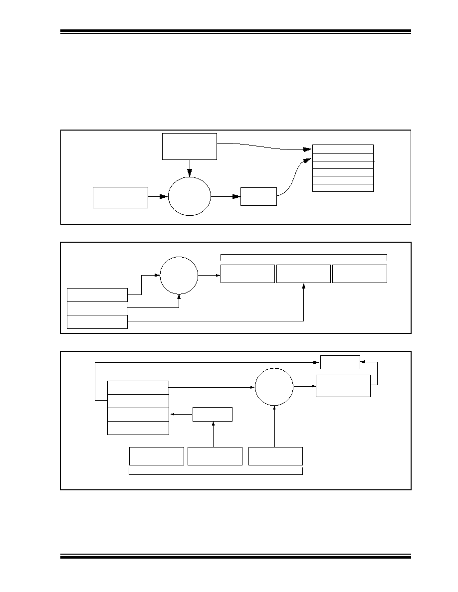
generation of the encryption key is done using a key
generation algorithm (Figure 1-1). Typically, inputs to
the key generation algorithm are the serial number of
the transmitter or seed value, and a 64-bit manufac-
turer's code. The manufacturer's code is chosen by the
system manufacturer and must be carefully controlled.
The manufacturer's code is a pivotal part of the overall
system security.
The 16-bit synchronization value is the basis for the
transmitted code changing for each transmission, and
is updated each time a button is pressed. Because of
the complexity of the code hopping encryption algo-
rithm, a change in one bit of the synchronization value
will result in a large change in the actual transmitted
code. There is a relationship (Figure 1-2) between the
key values in EEPROM and how they are used in the
encoder. Once the encoder detects that a button has
been pressed, the encoder reads the button and
updates the synchronization counter. The synchroniza-
tion value is then combined with the encryption key in
the encryption algorithm and the output is 32 bits of
encrypted information. This data will change with every
button press, hence, it is referred to as the hopping
portion of the code word. The 32-bit hopping code is
combined with the button information and the serial
number to form the code word transmitted to the
receiver. The code word format is explained in detail
in Section 4.2.
Any type of controller may be used as a receiver, but it
is typically a microcontroller with compatible firmware
that allows the receiver to operate in conjunction with a
transmitter, based on the HCS361. Section
7.0
provides more detail on integrating the HCS361 into a
total system.
*Secure Learning patents pending.
HCS361
©
1996 Microchip Technology Inc.
Preliminary
DS40146C-page 3
Before a transmitter can be used with a particular
receiver, the transmitter must be `learned' by the
receiver. Upon learning a transmitter, information is
stored by the receiver so that it may track the
transmitter, including the serial number of the
transmitter, the current synchronization value for that
transmitter and the same encryption key that is used on
the transmitter. If a receiver receives a message of valid
format, the serial number is checked and, if it is from a
learned transmitter, the message is decrypted and the
decrypted synchronization counter is checked against
what is stored. If the synchronization value is verified,
then the button status is checked to see what operation
is needed. Figure 1-3 shows the relationship between
some of the values stored by the receiver and the val-
ues received from the transmitter.
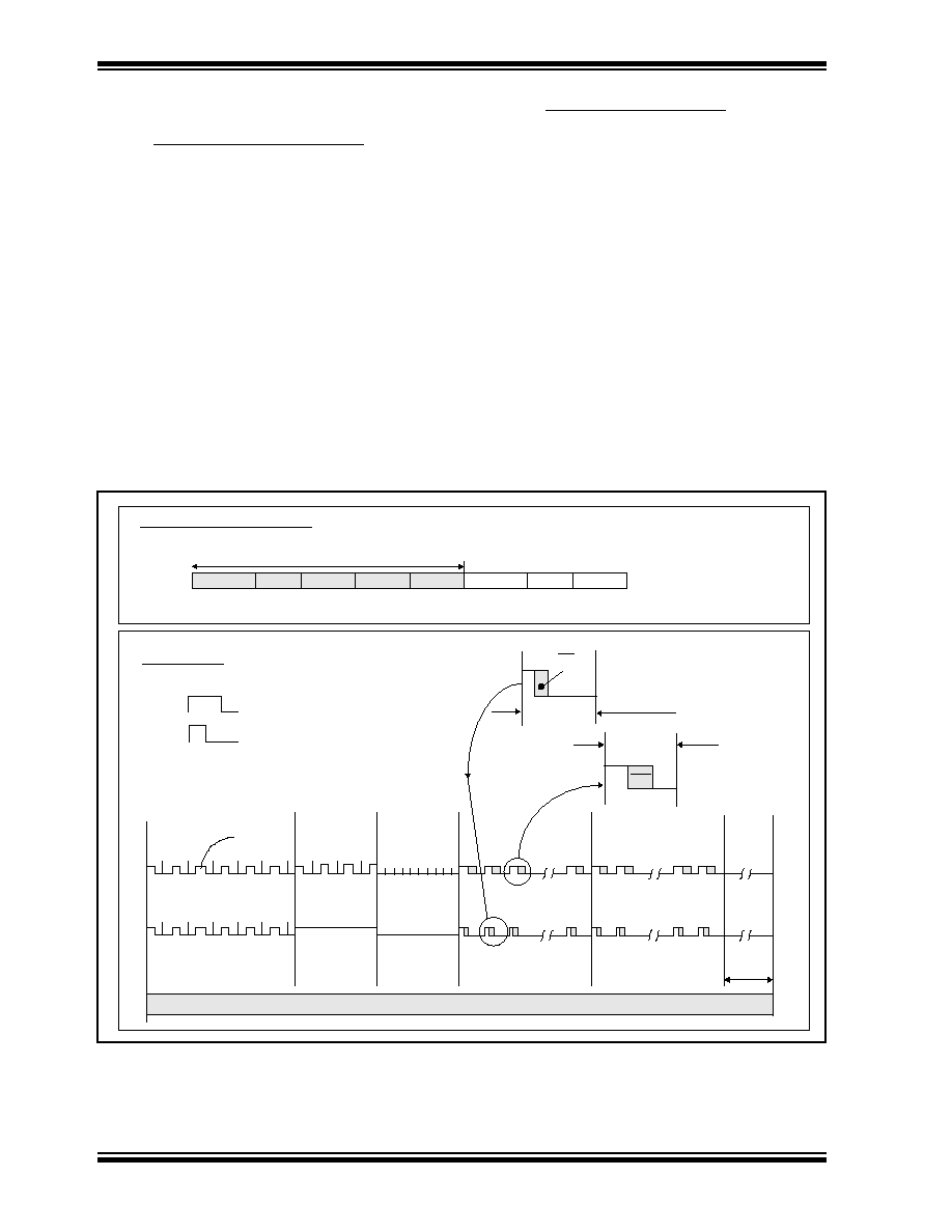
FIGURE 1-1:
CREATION AND STORAGE OF ENCRYPTION KEY DURING PRODUCTION
FIGURE 1-2:
BASIC OPERATION OF TRANSMITTER (ENCODER)
FIGURE 1-3:
BASIC OPERATION OF RECEIVER (DECODER)
Transmitter
Manufacturer's
Serial Number or
Code
Encryption
Key
Key
Generation
Algorithm
Serial Number
Encryption Key
Sync Counter
.
.
.
HCS361 EEPROM Array
Seed
K
EE
L
OQ
Algorithm
Button Press
Information
Encryption
EEPROM Array
32 Bits of
Encrypted Data
Serial Number
Transmitted Information
Decryption Key
Sync Counter
Serial Number
Button Press
Information
EEPROM Array
Decryption Key
32 Bits of
Encrypted Data
Serial Number
Received Information
Decrypted
Synchronization
Counter
Check for
Match
Check for
Match
K
EE
L
OQ
Algorithm
Decryption
Sync Counter
Serial Number
Manufacturer Code
HCS361
DS40146C-page 4
Preliminary
©
1996 Microchip Technology Inc.
2.0
DEVICE OPERATION
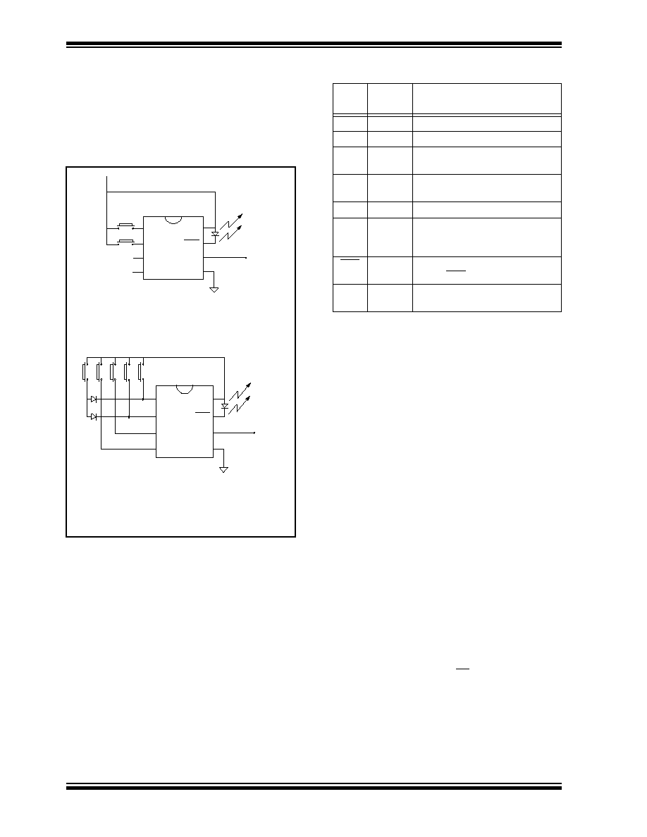
As shown in the typical application circuits (Figure 2-1),
the HCS361 is a simple device to use. It requires only
the addition of buttons and RF circuitry for use as the
transmitter in your security application. A description of
each pin is described in Table 2-1.
FIGURE 2-1:
TYPICAL CIRCUITS
TABLE 2-1
PIN DESCRIPTIONS
The high security level of the HCS361 is based on the
patented K
EE
L
OQ
technology. A block cipher type of
encryption algorithm based on a block length of 32 bits
and a key length of 64 bits is used. The algorithm
obscures the information in such a way that even if the
transmission information (before coding) differs by only
one bit from the information in the previous transmis-
sion, the next coded transmission will be totally differ-
ent. Statistically, if only one bit in the 32-bit string of
information changes, approximately 50 percent of the
coded transmission will change. The HCS361 will wake
up upon detecting a switch closure and then delay
approximately 6.5 ms for switch debounce (Figure 2-2).
The synchronization information, fixed information, and
switch information will be encrypted to form the hopping
code. The encrypted or hopping code portion of the
transmission will change every time a button is
pressed, even if the same button is pushed again.
Keeping a button pressed for a long time will result in
the same code word being transmitted until the button
is released or time-out occurs. A code that has been
transmitted will not occur again for more than 64K
transmissions. This will provide more than 18 years of
typical use before a code is repeated based on 10 oper-
ations per day. Overflow information programmed into
the encoder can be used by the decoder to extend the
number of unique transmissions to more than 128K.
If in the transmit process it is detected that a new but-
ton(s) has been pressed, a reset will immediately be
forced and the code word will not be completed. Please
note that buttons removed will not have any effect on
the code word unless no buttons remain pressed in
which case the current code word will be completed
and the power down will occur.
V
DD
B0
Tx out
S0
S1
S2
S3
LED
V
DD
PWM
V
SS
2 button remote control
B1
V
DD
Tx out
S0
S1
S2
S3
LED
V
DD
PWM
V
SS
5 button remote control (Note)
B4 B3 B2 B1 B0
Note:
Up to 15 functions can be implemented
by pressing more than one button simul-
Name
Pin
Number
Description
S0
1
Switch input 0
S1
2
Switch input 1
S2
3
Switch input 2/Can also be clock
pin when in programming mode
S3
4
Switch input 3/Clock pin when in
programming mode
V
SS
5
Ground reference connection
PWM
6
Pulse width modulation (PWM)
output pin/Data pin for
programming mode
LED
7
Cathode connection for directly
driving LED during transmission
V
DD
8
Positive supply voltage
connection
HCS361
©
1996 Microchip Technology Inc.
Preliminary
DS40146C-page 5
FIGURE 2-2:
ENCODER OPERATION
3.0
EEPROM MEMORY
ORGANIZATION
The HCS361 contains 192 bits (12 x 16-bit words) of
EEPROM memory (Table 3-1). This EEPROM array is
used to store the encryption key information,
synchronization value, etc. Further descriptions of the
memory array is given in the following sections.
TABLE 3-1
EEPROM MEMORY MAP
3.1
Key_0 - Key_3 (64-Bit Encryption Key)
The 64-bit encryption key is used by the transmitter to
create the encrypted message transmitted to the
receiver. This key is created and programmed at the
time of production using a key generation algorithm.
Inputs to the key generation algorithm are the serial
number for the particular transmitter being used and a
secret manufacturer's code. While the key generation
algorithm supplied from Microchip is the typical method
used, a user may elect to create their own method of
key generation. This may be done providing that the
decoder is programmed with the same means of creat-
ing the key for decryption purposes. If a seed is used,
the seed will also form part of the input to the key gen-
eration algorithm.
Power Up
Reset and Debounce Delay
(6.5 ms)
Sample Inputs
Update Sync Info
Encrypt With
Load Transmit Register
Buttons
Added
?
All
Buttons
Released
?
(A button has been pressed)
Transmit
Stop
No
Yes
No
Yes
Encryption Key
Complete Code
Word Transmission
WORD
ADDRESS
MNEMONIC
DESCRIPTION
0
KEY_0
64-bit encryption
key (word 0)
1
KEY_1
64-bit encryption
key (word 1)
2
KEY_2
64-bit encryption
key (word 2)
3
KEY_3
64-bit encryption
key (word 3)
4
SYNC_A
16-bit synchroni-
zation
value
5
SYNC_B/SEED_2
16-bit synchroni-
zation or seed
value (word 2)
6
RESERVED
Set to 0000H
7
SEED_0
Seed Value
(word 0)
8
SEED_1
Seed Value
(word 1)
7
SER_0
Device Serial
Number (word 0)
10
SER_1
Device Serial
Number (word 1)
11
CONFIG
Configuration
Word

HCS361
DS40146C-page 6
Preliminary
©
1996 Microchip Technology Inc.
3.2
SYNC_A, SYNC_B
(Synchronization Counter)
This is the 16-bit synchronization value that is used to
create the hopping code for transmission. This value
will be changed after every transmission. A second syn-
chronization value can be used to stay synchronized
with a second receiver.
3.3
SEED_0, SEED_1, and SEED_2
(Seed Word)
This is the three word (48 bits) seed code that will be
transmitted when seed transmission is selected. This
allows the system designer to implement the secure
learn feature or use this fixed code word as part of a dif-
ferent key generation/tracking process or purely as a
fixed code transmission.
3.4
SER_0, SER_1 (Encoder Serial
Number)
SER_0 and SER_1 are the lower and upper words of
the device serial number, respectively. There are 32 bits
allocated for the serial number and a selectable config-
uration bit determines whether 32 or 28 bits will be
transmitted. The serial number is meant to be unique
for every transmitter.
3.5
CONFIG (Configuration Word)
The configuration word is a 16-bit word stored in
EEPROM array that is used by the device to store
information used during the encryption process, as well
as the status of option configurations. Further
explanations of each of the bits are described in the
following sections.
TABLE 3-2
CONFIGURATION WORD
3.5.1
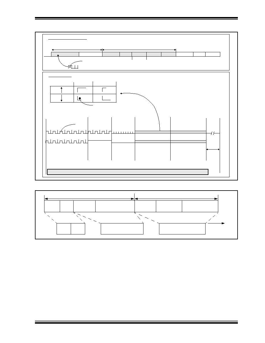
BACW: BLANK ALTERNATE CODE WORD
BACW = 1 selects the encoder to transmit every sec-
ond code word. This can be used to reduce the average
power transmitted over a 100ms window and thereby
transmit a higher peak power.
3.5.2
FAST: SELECT FAST TRANSMISSION
FAST selects the baud rate. If FAST = 1, the baud rate
is nominally 1667 bits per second and with FAST = 0,
833 bits per second.
3.5.3
TXWAK: BIT FORMAT SELECT OR
WAKEUP
In PWM mode, this bit selects the bit format. If TXWAK
= 1, the PWM pulse is 1/6;2/6 and for TXWAK = 0, 1/
3;2/3 (Figure 4-1, VPWM = 0).
In VPWM mode, this bit enables the wake-up signal.
With TXWAK = 1, transmission of the wake-up and
dead time sequence is enabled (Figure 4-2, VPWM =
1). Wakeup is transmitted before the first code word of
each transmission only. For TXWAK = 0, the transmis-
sion will skip wake-up and start transmitting the pream-
ble portion of the code word (Figure 4-2, VPWM = 1).
3.5.4
SPM: SYNC PULSE MODULATION
Select modulation mode of Sync Pulse. If SPM = 1, the
sync pulse is modulated (Figure 4-1 and Figure 4-2).
Bit Number
Symbol
Bit Description
0
BACW
Blank Alternate Code Word
1
FAST
Baud Rate Selection
2
TXWAK
PWM mode: 1/6, 2/6 or 1/3,
2/3 select
VPWM mode: Wakeup
enable
3
SPM
Sync Pulse Modulation
4
SEED
Seed Transmission enable
5
DELM
Delay mode enable
6
TIMO
Time out enable
7
IND
Independent mode enable
8
USRA0
User bit
9
USRA1
User bit
10
USRB0
User bit
11
USRB1
User bit
12
XSER
Extended serial number
enable
13
TMPSD
Temporary seed transmis-
sion enable
14
VPWM
VPWM select
15
OVR
Overflow bit

HCS361
©
1996 Microchip Technology Inc.
Preliminary
DS40146C-page 7
3.5.5
SEED: ENABLE SEED TRANSMISSION
If SEED = 0, seed transmission is disabled. The inde-
pendent counter mode can only be used with seed
transmission disabled since SEED_2 is shared with the
second synchronization counter.
With SEED = 1, seed transmission is enabled. The
appropriate button code(s) must be activated to trans-
mit the seed information. In this mode, the seed infor-
mation (SEED_0, SEED_1, and SEED_2) and the
upper 12- or 16-bits of the serial number (SER_1)are
transmitted instead of the hop code.
Seed transmission is available for function codes
(Table 3-7) S[3:0] = 1001 and S[3:0] = 0011 (delayed).
This takes place regardless of the setting of the IND bit.
The two seed transmissions are shown in Figure 3-1.
FIGURE 3-1:
SEED TRANSMISSION
All examples shown with XSER = 1, SEED = 1
When S[3:0] = 1001, delay is not applicable.
CRC+V
LOW
SER_1
SEED_2
SEED_1
SEED_0
Data transmission direction
For S[3:0] = 0x3 before delay:
16-bit Data Word
16-bit Counter
Encrypt
CRC+V
LOW
SER_1
SER_0
Encrypted Data
For S[3:0] = 0011 after delay (Note 1, Note 2):
CRC+V
LOW
SER_1
SEED_2
SEED_1
SEED_0
Data transmission direction
Data transmission direction
Note 1: For Seed Transmission, SEED_2 is transmitted instead of SER_0.
2: For Seed Transmission, the setting of DELM has no effect.

HCS361
DS40146C-page 8
Preliminary
©
1996 Microchip Technology Inc.
3.5.6
DELM: DELAY MODE
If DELM = 1, delay transmission is enabled. A delayed
transmission is indicated by inverting the lower nibble of
the discrimination value. The delay mode is primarily for
compatibility with previous K
EE
L
OQ
devices. If
DELM
=
0, delay transmission is disabled (Table 3-3).
TABLE 3-3
TYPICAL DELAY TIMES
3.5.7
TIMO: TIME-OUT
If TIMO = 1, the time-out is enabled. Time-out can be
used to terminate accidental continuous transmissions.
When time-out occurs, the PWM output is set low and
the LED is turned off. Current consumption will be
higher than in standby mode since current will flow
through the activated input resistors. This state can be
exited only after all inputs are taken low. TIMO = 0, will
enable continuous transmission (Table 3-4).
TABLE 3-4
TYPICAL TIME-OUT TIMES
3.5.8
IND: INDEPENDENT MODE
The independent mode can be used where one
encoder is used to control two receivers. Two counters
(SYNC_A and SYNC_B) are used in independent
mode. As indicated in Table 3-7, function codes 1 to 7
use SYNC_A and 8 to 15 SYNC_B. The independent
mode also selects IR mode. In IR mode function codes
12 to 15 will use counter B. The PWM output signal is
modulated with a 40 kHz carrier. It must be pointed out
the 40 kHz is derived from the internal clock and will
therefore vary with the same percentage as the baud
rate. If IND = 0, SYNC_A is used for all function codes.
If IND = 1, independent mode is enabled and counters
for functions are used according to Table 3-7.
For IND = 1 and S[3:0]
0xC, 0xD, 0xE, 0xF, Basic
Pulse Width modulation becomes:
TABLE 3-5
IR MODULATION
3.5.9
USRA,B: USER BITS
User bits form part of the discrimination value. The user
bits together with the IND bit can be used to identify the
counter that is used in independent mode.
3.5.10
XSER: EXTENDED SERIAL NUMBER
If XSER = 1, the full 32-bit serial number [SER_1,
SER_0] is transmitted. If XSER = 0, the four most sig-
nificant bits of the serial number are substituted by
S[3:0] and is compatible with the HCS200/300/301.
3.5.11
TMPSD: TEMPORARY SEED
TRANSMISSION
The temporary seed transmission can be used to dis-
able learning after the transmitter has been used for a
programmable number of operations. This feature can
be used to implement very secure systems. After learn-
ing is disabled, the seed information cannot be
accessed even if physical access to the transmitter is
possible. If TMPSD = 1 the seed transmission will be
disabled after a number of code hopping transmissions.
The number of transmissions before seed transmission
is disabled, can be programmed by setting the synchro-
nization counter (SYNC_A or SYNC_B) to a value as
shown in Table 3-6.
TABLE 3-6
SYNCHRONOUS COUNTER
INITIALIZATION VALUES
TXWAK
FAST
Number of
Code Words
before Delay
Mode
Time Before
Delay Mode
(VPWM = 0)
0
0
28
2.8s
0
1
56
2.9s
1
0
28
2.6s
1
1
56
2.8s
TXWAK FAST
Maximum
Number of
Code Words
Transmitted
Time Before
Time-out
(VPWM = 0)
0
0
256
25.6s
0
1
512
27.2s
1
0
256
23.8s
1
1
512
25.4s
TXWAK
FAST
Basic Pulse
0
0
0
1
1
0
1
1
Synchronous Counter
Values
Number of
Transmissions
0000H
128
0060H
64
0050H
32
0048H
16
(400
µ
s)
(16x)
(200
µ
s)
(8x)
Period = 25
µ
s
(100
µ
s)
(8x)

HCS361
©
1996 Microchip Technology Inc.
Preliminary
DS40146C-page 9
TABLE 3-7
FUNCTION CODES
3.5.12
VPWM: VARIABLE PULSE WIDTH
MODULATION
VPWM selects between VPWM modulation and PWM
modulation. If VPWM = 1, VPWM modulation is
selected as well as the following:
1.
Enables the TXWAK bit to select the WAKEUP
transmission.
2.
Extends the Guard Time.
If VPWM = 0, PWM modulation is selected.
3.5.13
OVR: OVERFLOW
The overflow bit is used to extend the number of possi-
ble synchronization values. The synchronization
counter is 16 bits in length, yielding 65,536 values
before the cycle repeats. Under typical use of
10
operations a day, this will provide nearly 18 years of
use before a repeated value will be used. Should the
system designer conclude that is not adequate, then
the overflow bit can be utilized to extend the number of
unique values. This can be done by programming OVR
to 1 at the time of production. The encoder will automat-
ically clear OVR the first time that the transmitted syn-
chronization value wraps from 0xFFFF to 0x0000.
Once cleared, OVR cannot be set again, thereby creat-
ing a permanent record of the counter overflow. This
prevents fast cycling of 64K counter. If the decoder sys-
tem is programmed to track the overflow bits, then the
effective number of unique synchronization values can
be extended to 128K. If programmed to zero, the sys-
tem will be compatible with the NTQ104/5/6 devices
(i.e., no overflow with discrimination bits set to zero).
S3
S2
S1
S0
IND = 0
IND = 1
Comments
Counter
1
0
0
0
1
A
A
2
0
0
1
0
A
A
3
0
0
1
1
A
A
If SEED = 1, transmit seed after delay.
4
0
1
0
0
A
A
5
0
1
0
1
A
A
6
0
1
1
0
A
A
7
0
1
1
1
A
A
8
1
0
0
0
A
B
9
1
0
0
1
A
B
If SEED = 1, transmit seed immediately.
10
1
0
1
0
A
B
11
1
0
1
1
A
B
12
1
1
0
0
A
B IR mode
13
1
1
0
1
A
B IR mode
14
1
1
1
0
A
B IR mode
15
1
1
1
1
A
B IR mode
HCS361
DS40146C-page 10
Preliminary
©
1996 Microchip Technology Inc.
4.0
TRANSMITTED WORD
4.1
Transmission Format (PWM)
The HCS361 transmission is made up of several parts
(Figure 4-1 and Figure
4-2). Each transmission is
begun with a preamble and a header, followed by the
encrypted and then the fixed data. The actual data is
67 bits which consists of 32 bits of encrypted data and
35 bits of fixed data. Each transmission is followed by
a guard period before another transmission can begin.
Refer to Table and Table for transmission timing spec-
ifications. The encrypted portion provides up to four bil-
lion changing code combinations and includes the
function bits (based on which buttons were activated)
along with the synchronization counter value and dis-
crimination value. The non-encrypted portion is com-
prised of the CRC bits, V
LOW
bits, the function bits and
the 28/32-bit serial number. The encrypted and non-
encrypted sections combined increase the number of
combinations to 1.47 x 10
20
.
4.2
Code Word Organization
The HCS361 transmits a 67-bit code word when a but-
ton is pressed. The 67-bit word is constructed from a
Fixed Code portion and an Encrypted Code portion
(Figure 4-3).
The Encrypted Data is generated from 4 function bits,
2 user bits, overflow bit, independent mode bit, and 8
serial number bits, and the 16-bit synchronization value
(Figure 8-4).
The Non-encrypted Code Data is made up of V
LOW
bit, 2 CRC bits, 4 function bits, and the 28-bit serial
number. If the extended serial number (32 bits) is
selected, the 4 function code bits will not be transmit-
ted.
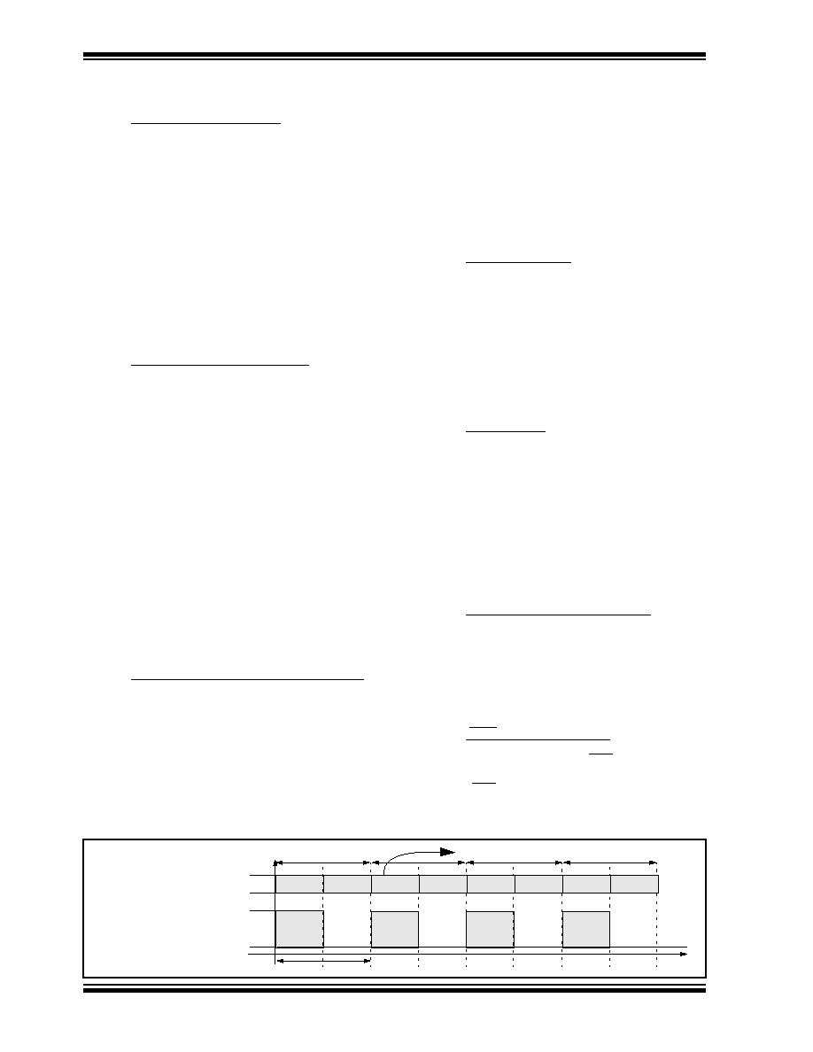
FIGURE 4-1:
TRANSMISSION FORMAT--VPWM = 0
T
BP
LOGIC "1"
Code Word
BIT
T
E
Guard
Time
TXWAK=1
TXWAK=0
SPM=1
SPM=0
Preamble
Header
Encrypted
Data
Fixed Code
Data
BIT
LOGIC "0"
TXWAK=1
TXWAK=0
T
BP
CODE WORD:
TRANSMISSION SEQUENCE:
Preamble
Sync
Encrypt
Fixed
Guard
1 CODE WORD
Preamble
Sync
Encrypt
∑
HCS361
©
1996 Microchip Technology Inc.
Preliminary
DS40146C-page 11
FIGURE 4-2:
TRANSMISSION FORMAT--VPWM = 1
FIGURE 4-3:
CODE WORD ORGANIZATION (RIGHT-MOST BIT IS CLOCKED-OUT FIRST)
Guard
Time
SPM=1
SPM=0
Preamble
Header
Encrypted
Data
Fixed Code
Data
LOGIC "0"
T
E
CODE WORD:
TOTAL TRANSMISSION:
WAKEUP (OPTION)
Preamble Sync
Encrypt
Fixed
Guard
x84
Dead Time
1 CODE WORD
Preamble Sync Encrypt
Te
LOGIC "1"
TRANSITION
Te
∑
Code Word
LSB
MSB
Fixed Code Data
Encrypted Code Data
67 bits
of Data
Transmitted
MSB
LSB
CRC
(2 bit)
V
LOW
(1 bit)
Button
Status
(4 bits)
28-bit
Serial Number
Button
Status
(4 bits)
Discrimination
bits
(12 bits)
16-bit
Synch Value
CRC
(2 bit)
V
LOW
bit
+
Serial Number and
Button Status (32 bits)
+
32 bits of Encrypted Data
HCS361
DS40146C-page 12
Preliminary
©
1996 Microchip Technology Inc.
5.0
SPECIAL FEATURES
5.1
Code Word Completion
Code word completion is an automatic feature that
ensures that the entire code word is transmitted, even
if the button is released before the transmission is com-
plete and that a minimum of two words are completed.
The HCS361 encoder powers itself up when a button is
pushed and powers itself down after the current trans-
mission is finished, if the user has already released the
button. If the button is held down beyond the time for
two transmissions, then multiple transmissions will
result. The HCS361 transmits at least two transmis-
sions before powering down. If another button is acti-
vated during a transmission, the active transmission will
be aborted and the new code will be generated using
the new button information.
5.2
Blank Alternate Code Word
Federal Communications Commission (FCC) part 15
rules specify the limits on fundamental power and
harmonics that can be transmitted. Power is calculated
on the worst case average power transmitted in a
100ms window. It is therefore advantageous to
minimize the duty cycle of the transmitted word. This
can be achieved by minimizing the duty cycle of the
individual bits and by blanking out consecutive words.
Blank Alternate Code Word (BACW) is used for
reducing the average power of a transmission
(Figure
5-1). This is a selectable feature. Using the
BACW allows the user to transmit a higher amplitude
transmission if the transmission length is shorter. The
FCC puts constraints on the average power that can be
transmitted by a device, and BACW effectively prevents
continuous transmission by only allowing the transmis-
sion of every second word. This reduces the average
power transmitted and hence, assists in FCC approval
of a transmitter device.
5.3
CRC (Cycle Redundancy Check) Bits
The CRC bits are calculated on the 65 previously trans-
mitted bits. The CRC bits can be used by the receiver
to check the data integrity before processing starts. The
CRC can detect all single bit and 66% of double bit
errors. The CRC is computed as follows:
EQUATION 0-1:
CRC CALCULATION
and
with
and
Di
n
the nth transmission bit 0
n
64
5.4
Secure Learning
In order to increase the level of security in a system, it
is possible for the receiver to implement what is known
as a secure learning function. This can be done by uti-
lizing the seed value on the HCS361 which is stored in
EEPROM. Instead of the normal key generation
method being used to create the encryption key, this
seed value is used and there should not be any mathe-
matical relationship between serial numbers and seeds
for the best security.
5.5
Auto-shutoff
The Auto-shutoff function automatically stops the
device from transmitting if a button inadvertently gets
pressed for a long period of time. This will prevent the
device from draining the battery if a button gets pressed
while the transmitter is in a pocket or purse. This func-
tion can be enabled or disabled and is selected by set-
ting or clearing the time-out bit (Section 3.5.7). Setting
this bit will enable the function (turn Auto-shutoff func-
tion on) and clearing the bit will disable the function.
Time-out period is approximately 25 seconds.
5.6
V
LOW
: Voltage LOW Indicator
The V
LOW
bit is transmitted with every transmission
(Figure 4-2) and will be transmitted as a one if the
operating voltage has dropped below the low voltage
trip point, typically 3.8V at 25
∞
C. This V
LOW
signal is
transmitted so the receiver can give an indication to the
user that the transmitter battery is low.
5.7
LED Output Operation
During normal transmission the LED output is LOW. If
the supply voltage drops below the low voltage trip
point, the LED output will be toggled at approximately
1Hz during the transmission.
FIGURE 5-1:
BLANK ALTERNATE CODE WORD
CRC 1
[ ]
n
1
+
CRC 0
[ ]
n
Di
n
=
CRC 0
[ ]
n
1
+
CRC 0
[ ]
n
Di
n
(
)
CRC 1
[ ]
n
=
CRC 1 0
,
[
]
0
0
=
One Code Word
BACW Disabled
(All words transmitted)
BACW Enabled
(1 out of 2 transmitted)
A
2A
100ms
100ms
100ms
100ms
Amplitude
Time
Min Tx Length
HCS361
©
1996 Microchip Technology Inc.
Preliminary
DS40146C-page 13
6.0
PROGRAMMING THE HCS361
When using the HCS361 in a system, the user will have
to program some parameters into the device including
the serial number and the secret key before it can be
used. The programming cycle allows the user to input
all 192 bits in a serial data stream, which are then
stored internally in EEPROM. Programming will be
initiated by forcing the PWM line high, after the S3 line
has been held high for the appropriate length of time.
S0 and S1 should be held low during the entire program
cycle (Table 6-1 and Figure 6-1). The device can then
be programmed by clocking in 16 bits at a time, followed
by the word's complement using S3 or S2 as the clock
line and PWM as the data in line. After each 16-bit word
is loaded, a programming delay is required for the
internal program cycle to complete. An acknowledge bit
can be read back after the programming delay (T
WC
).
After the first word and its complement have been
downloaded, an automatic bulk write is performed. This
delay can take up to Twc. At the end of the program-
ming cycle, the device can be verified (Figure 6-2) by
reading back the EEPROM. Reading is done by clock-
ing the S3 line and reading the data bits on PWM. For
security reasons, it is not possible to execute a verify
function without first programming the EEPROM. A
verify operation can only be done once, immedi-
ately following the program cycle.
FIGURE 6-1:
PROGRAMMING WAVEFORMS
FIGURE 6-2:
VERIFY WAVEFORMS
TABLE 6-1
PROGRAMMING/VERIFY TIMING REQUIREMENTS
V
DD
= 5.0V
±
10%
25
∞
C
±
5
∞
C
Parameter
Symbol
Min.
Max.
Units
Program mode setup time
T
2
0
4.9
ms
Hold time 1
T
1
9.0
--
ms
Programming delay
T
WC
--
30
ms
Clock low time
T
CLKL
25
--
µ
s
Clock high time
T
CLKH
25
--
µ
s
Data setup time
T
DS
0
--
µ
s
Data hold time
T
DH
18
--
µ
s
Data out valid time
T
DV
--
24
µ
s
PWM
Enter Program
Mode
(Data)
(Clock)
Bit 0
Bit 1
Bit 2
Bit 3
Bit 14 Bit 15
Bit 16 Bit 17
T
1
T
2
Repeat 12 times for each word
T
CLKH
T
CLKL
T
WC
T
DS
S2/S3
Data for Word 0 (KEY_0)
Data for Word 1
T
DH
Bit 0
Bit 1
Bit 2
Bit 3
Bit 14 Bit 15
Note 1: Unused button inputs to be held to ground during the entire programming sequence.
2: The V
DD
pin must be taken to ground after a program/verify cycle.
Acknowledge
PWM
(Clock)
(Data)
Note: If a Verify operation is to be done, then it must immediately follow the Program cycle.
End of
Programming Cycle
Begin Verify Cycle Here
Bit 1 Bit 2
Bit 3
Bit 15
Bit 14
Bit 16 Bit 17
Bit190 Bit191
T
WC
Data in Word 0
T
DV
S2/S3
Bit 0
Bit191
Bit190
HCS361
DS40146C-page 14
Preliminary
©
1996 Microchip Technology Inc.
7.0
INTEGRATING THE HCS361
INTO A SYSTEM
Use of the HCS361 in a system requires a compatible
decoder. This decoder is typically a microcontroller with
compatible firmware. Firmware routines that accept
transmissions from the HCS361 and decrypt the
hopping code portion of the data stream are available.
These routines provide system designers the means to
develop their own decoding system.
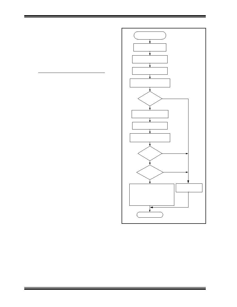
7.1
Learning a Transmitter to a Receiver
In order for a transmitter to be used with a decoder, the
transmitter must first be `learned'. Several learning
strategies can be followed in the decoder implementa-
tion. When a transmitter is learned to a decoder, it is
suggested that the decoder stores the serial number
and current synchronization value in EEPROM. The
decoder must keep track of these values for every
transmitter that is learned (Figure 7-1). The maximum
number of transmitters that can be learned is only a
function of how much EEPROM memory storage is
available. The decoder must also store the manufac-
turer's code in order to learn a transmission transmitter,
although this value will not change in a typical system
so it is usually stored as part of the microcontroller
ROM code. Storing the manufacturer's code as part of
the ROM code is also better for security reasons.
It must be stated that some learning strategies have
been patented and care must be taken not to infringe.
FIGURE 7-1:
TYPICAL LEARN SEQUENCE
Enter Learn
Mode
Wait for Reception
of a Valid Code
Generate Key
from Serial Number
Use Generated Key
to Decrypt
Compare Discrimination
Value with Fixed Value
Equal
Wait for Reception
of Second Valid Code
Compare Discrimination
Value with Fixed Value
Use Generated Key
to Decrypt
Equal
Counters
Encryption key
Serial number
Synchronization counter
Sequential
?
?
?
Exit
Learn successful Store:
Learn
Unsuccessful
No
No
No
Yes
Yes
Yes
HCS361
©
1996 Microchip Technology Inc.
Preliminary
DS40146C-page 15
7.2
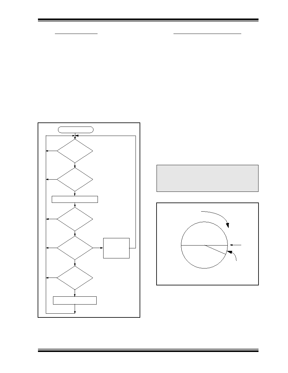
Decoder Operation
In a typical decoder operation (Figure 7-2), the key gen-
eration on the decoder side is done by taking the serial
number from a transmission and combining that with
the manufacturer's code to create the same secret key
that was used by the transmitter. Once the secret key is
obtained, the rest of the transmission can be decrypted.
The decoder waits for a transmission and immediately
can check the serial number to determine if it is a
learned transmitter. If it is, it takes the encrypted portion
of the transmission and decrypts it using the stored key
It uses the discrimination bits to determine if the
decryption was valid. If everything up to this point is
valid, the synchronization value is evaluated.
FIGURE 7-2:
TYPICAL DECODER
OPERATION
7.3
Synchronization with Decoder
The K
EE
L
OQ
technology features a sophisticated
synchronization technique (Figure 7-3) which does not
require the calculation and storage of future codes. If
the stored counter value for that particular transmitter
and the counter value that was just decrypted are within
a formatted window of say 16, the counter is stored and
the command is executed. If the counter value was not
within the single operation window, but is within the
double operation window of say 32K window, the trans-
mitted synchronization value is stored in temporary
location and it goes back to waiting for another trans-
mission. When the next valid transmission is received,
it will check the new value with the one in temporary
storage. If the two values are sequential, it is assumed
that the counter had just gotten out of the single opera-
tion `window', but is now back in sync, so the new syn-
chronization value is stored and the command
executed. If a transmitter has somehow gotten out of
the double operation window, the transmitter will not
work and must be relearned. Since the entire window
rotates after each valid transmission, codes that have
been used are part of the `blocked' (32K) codes and are
no longer valid. This eliminates the possibility of grab-
bing a previous code and retransmitting to gain entry.
FIGURE 7-3:
SYNCHRONIZATION WINDOW
?
Transmission
Received
Does
Serial Number
Match
?
Decrypt Transmission
Is
Decryption
Valid
?
Is
Counter
Within 16
?
Is
Counter
Within 32K
?
Update
Counter
Execute
Command
Save Counter
in Temp Location
Start
No
No
No
No
Yes
Yes
Yes
Yes
Yes
No
and
No
Note:
The synchronization method described in
this section is only a typical implementation
and because it is usually implemented in
firmware, it can be altered to fit the needs
of a particular system
Blocked
Entire Window
rotates to eliminate
use of previously
used codes
Current
Position
(32K Codes)
Double
Operation
(32K Codes)
Single Operation
Window (16 Codes)

HCS361
DS40146C-page 16
Preliminary
©
1996 Microchip Technology Inc.
8.0
ELECTRICAL CHARACTERISTICS
TABLE 8-1
ABSOLUTE MAXIMUM RATINGS
TABLE 8-2
DC CHARACTERISTICS
Symbol
Item
Rating
Units
V
DD
Supply voltage
-0.3 to 6.9
V
V
IN
Input voltage
-0.3 to V
DD
+ 0.3
V
V
OUT
Output voltage
-0.3 to V
DD
+ 0.3
V
I
OUT
Max output current
25
mA
T
STG
Storage temperature
-55 to +125
∞
C (Note)
T
LSOL
Lead soldering temp
300
∞
C (Note)
V
ESD
ESD rating
4000
V
Note:
Stresses above those listed under "ABSOLUTE MAXIMUM RATINGS" may cause permanent damage to the
device.
Commercial
(C): Tamb = 0
∞
C to +70
∞
C
Industrial
(I): Tamb = -40
∞
C to +85
∞
C
2.0V < V
DD
< 3.3
3.0 < V
DD
< 6.6
Parameter
Sym.
Min
Typ
1
Max
Min
Typ
1
Max
Unit
Conditions
Operating current (avg)
I
CC
0.3
1.2
0.7
1.6
mA V
DD
= 3.3V
V
DD
= 6.6V
Standby current
I
CCS
0.1
1.0
0.1
1.0
µ
A
Auto-shutoff current
2,3
I
CCS
40
75
160
350
µ
A
High level Input voltage
V
IH
0.55V
DD
V
DD
+0.3 0.55V
DD
V
DD
+0.3
V
Low level input voltage
V
IL
-0.3
0.15V
DD
-0.3
0.15V
DD
V
High level output voltage
V
OH
0.7V
DD
0.7V
DD
V
I
OH
= -1.0mA, V
DD
= 2.0V
I
OH
= -2.0mA, V
DD
= 6.6V
Low level output voltage
V
OL
0.08V
DD
0.08V
DD
V
I
OL
= 1.0mA, V
DD
= 2.0V
I
OL
= 2.0mA, V
DD
= 6.6V
LED sink current
I
LED
0.15
1.0
4.0
0.15
1.0
4.0
mA Vled = 1.5V, V
DD
= 6.6V
Resistance; S0-S3
R
S
0-3
40
60
80
40
60
80
K
V
DD
= 4.0V
Resistance; PWM
R
PWM
80
120
160
80
120
160
K
V
DD
= 4.0V
Note 1: Typical values are at 25
∞
C.
2: Auto-shutoff current specification does not include the current through the input pulldown resistors.
3: Auto-shutoff current is periodically sampled and not 100% tested.
HCS361
©
1996 Microchip Technology Inc.
Preliminary
DS40146C-page 17
FIGURE 8-1:
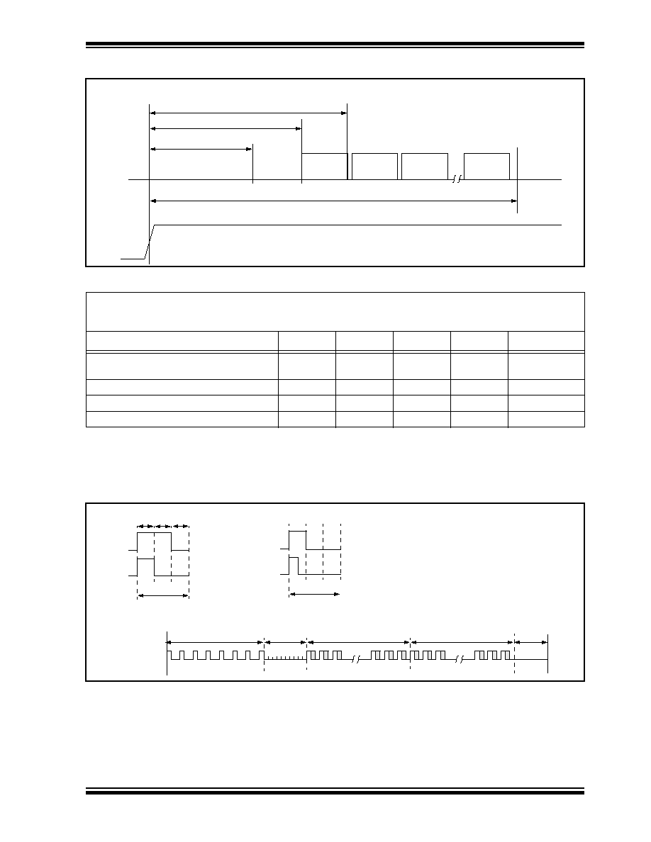
POWER UP AND TRANSMIT TIMING
TABLE 8-3
POWER UP AND TRANSMIT TIMING REQUIREMENTS
FIGURE 8-2:
PWM FORMAT SUMMARY (VPWM = 0)
V
DD
= +2.0 to 6.6V
Commercial
(C): Tamb = 0
∞
C to +70
∞
C
Industrial
(I): Tamb = -40
∞
C to +85
∞
C
Parameter
Symbol
Min
Max
Unit
Remarks
Time to second button press
T
BP
10 + Code
Word Time
26 + Code
Word Time
ms
(Note 1)
Transmit delay from button detect
T
TD
4.5
26
ms
(Note 2)
Debounce delay
T
DB
4
13
ms
Auto-shutoff time-out period
T
TO
15
35
s
(Note 3)
Note 1: T
BP
is the time in which a second button can be pressed without completion of the first code word and the
intention was to press the combination of buttons.
2: Transmit delay maximum value if the previous transmission was successfully transmitted.
3: The auto shutoff timeout period is not tested.
Button Press
Sn
Detect
T
DB
PWM
T
TD
Code Word Transmission
T
TO
Code
Word
1
Code
Word
2
Code
Word
3
Code
Word
n
T
BP
LOGIC `0'
LOGIC `1'
Preamble
Header
Encrypted Portion
of Transmission
Fixed portion of
Transmission
Guard
Time
T
P
T
H
T
HOP
T
FIX
T
G
T
BP
T
E
T
E
T
E
TXWAK = 0
T
BP
TXWAK = 1
LOGIC `0'
LOGIC `1'
HCS361
DS40146C-page 18
Preliminary
©
1996 Microchip Technology Inc.
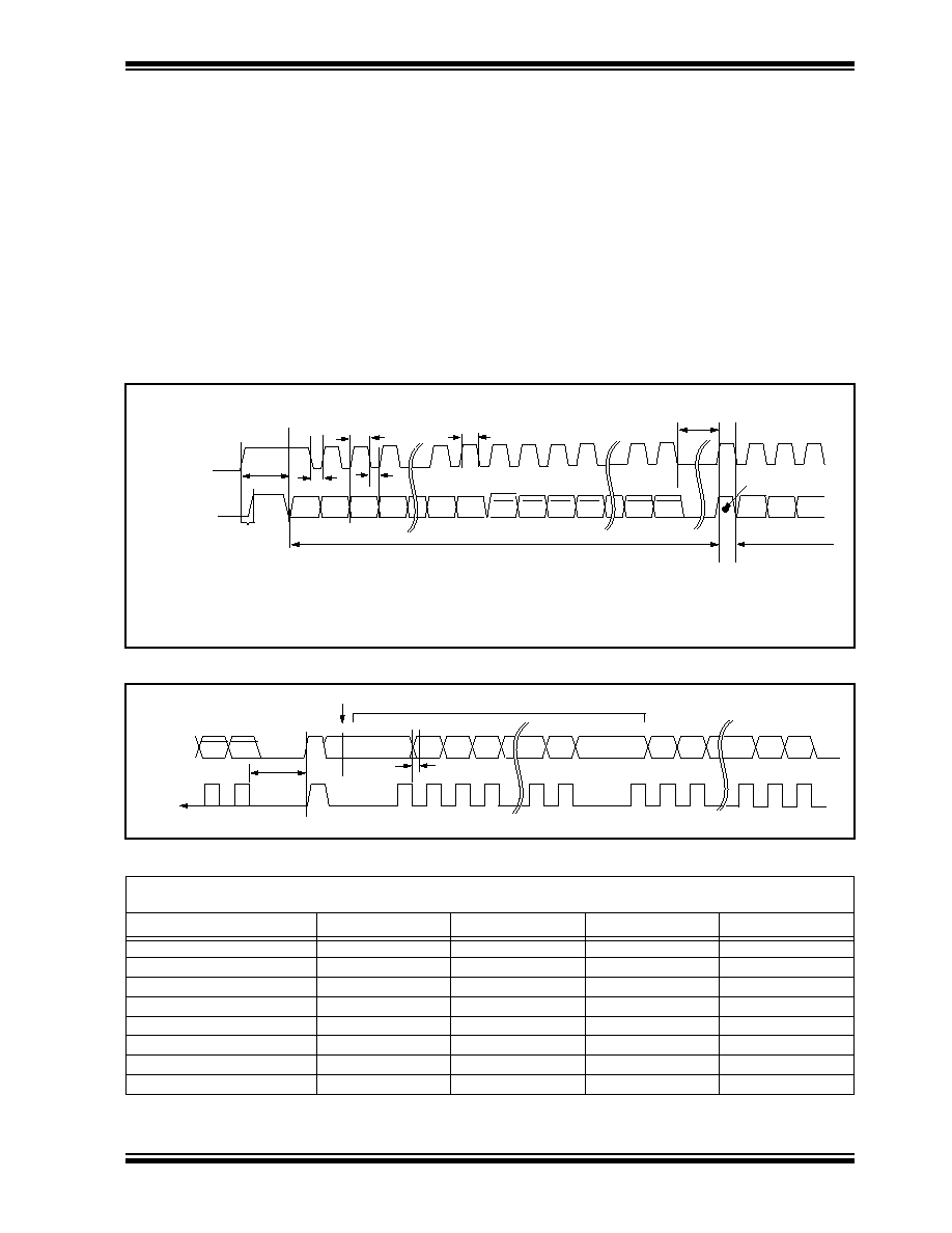
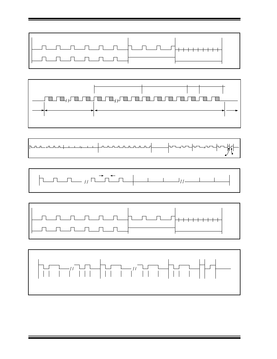
FIGURE 8-3:
PWM PREAMBLE/HEADER FORMAT
FIGURE 8-4:
PWM DATA WORD FORMAT
FIGURE 8-5:
VPWM FORMAT SUMMARY (VPWM = 1)
FIGURE 8-6:
VPWM WAKEUP FORMAT
FIGURE 8-7:
VPWM PREAMBLE/HEADER FORMAT
FIGURE 8-8:
VPWM DATA WORD FORMAT
Preamble
SPM = 0
Header
SPM = 1
10Te
30Te
10Te
Bit 0
Bit 1
Header
Bit 30 Bit 31 Bit 32 Bit 33
Bit 58 Bit 59
Fixed Code Data
Encrypted Data
Guard
LSB
LSB
MSB
MSB
S3
S0
S1
S2
V
LOW
CRC0 CRC1
Time
Serial Number
Function Code
Status
Bit 60 Bit 61 Bit 62 Bit 63 Bit 64 Bit 65
CRC
Bit 66
Wakeup
Dead Time
Preamble
Encrypt
Serial Number Function
Header
V
LOW
CRC
Wakeup
Dead Time
252 T
E
256 T
E
T
E
Preamble
SPM = 0
Header
SPM = 1
10Te
30Te
10Te
1 0
0
1
0 1
2
3
1 0 1
1
28 29 30 31
1 0
0
1
28 29
30
31
1 0
0
1
56 57
58
59
1 0
0
1
60 61
62
63
1 0
64 65
1
66
Encrypted Data
Serial Number
Function Code
V
LOW
CRC
Note:
The bit values are only shown as an example.
bit
HCS361
©
1996 Microchip Technology Inc.
Preliminary
DS40146C-page 19
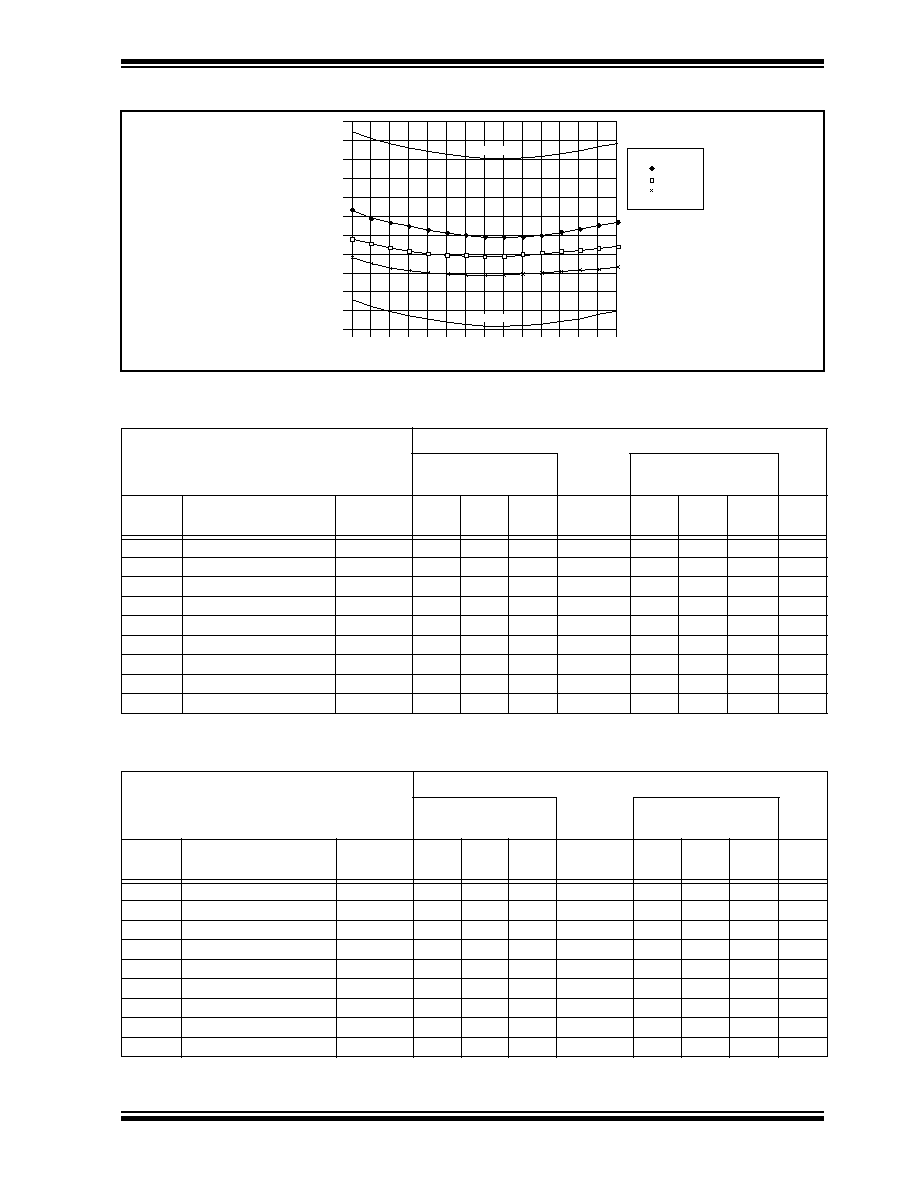
FIGURE 8-9:
HCS361 NORMALIZED TE VS. TEMP
0.8
1.7
1.6
1.5
1.4
1.3
1.2
1.1
1.0
0.9
0.7
0.6
T
E
Min.
T
E
Max.
V
DD
LEGEND
= 2.0V
= 3.0V
= 6.0V
Typical
T
E
Temperature
∞
C
-50 -40 -30 -20 -10 0
10 20 30 40 50 60 70 80 90
TABLE 8-4
CODE WORD TRANSMISSION TIMING PARAMETERS
PWM Mode (TXWAK = 0)
V
DD
= +2.0 to 6.6V
Commercial (C):Tamb = 0
∞
C to +70
∞
C
Industrial
(I):Tamb = -40
∞
C to +85
∞
C
Code Words Transmitted
FAST = 0,
TXWAK = 0
FAST = 1,
TXWAK = 0
Symbol
Characteristic
Number
of T
E
Min
Typ.
Max.
Number
of T
E
Min.
Typ.
Max.
Units
T
E
Basic pulse element
1
260
400
620
1
130
200
310
µ
s
T
BP
PWM bit pulse width
3
780
1200
1860
3
390
600
930
µ
s
T
P
Preamble duration
28
7.3
11.2
17.4
28
3.6
5.6
8.7
ms
T
H
Header duration
10
2.6
4.0
6.2
10
1.3
2.0
3.1
ms
T
HOP
Hopping code duration
96
25.0
38.4
59.5
96
12.5
19.2
29.8
ms
T
FIX
Fixed code duration
105
27.3
42.0
65.1
105
13.7
21.0
32.6
ms
T
G
Guard Time
16
4.2
6.4
9.9
32
4.2
6.4
9.9
ms
Total Transmit Time
255
66.3
102.0
158.1
271
35.2
54.2
84.0
ms
PWM data rate
1282
833
538
2564
1667
1075
bps
Note:
The timing parameters are not tested but derived from the oscillator clock.
PWM Mode (TXWAK = 1)
V
DD
= +2.0 to 6.6V
Commercial (C):Tamb = 0
∞
C to +70
∞
C
Industrial
(I):Tamb = -40
∞
C to +85
∞
C
Code Words Transmitted
FAST = 0,
TXWAK = 1
FAST = 1,
TXWAK = 1
Symbol
Characteristic
Number
of T
E
Min
Typ.
Max.
Number
of T
E
Min.
Typ.
Max.
Units
T
E
Basic pulse element
1
130
200
310
1
65
100
155
µ
s
T
BP
PWM bit pulse width
6
780
1200
1860
6
390
600
930
µ
s
T
P
Preamble duration
28
3.6
5.6
8.7
28
1.8
2.8
4.3
ms
T
H
Header duration
10
1.3
2.0
3.1
10
0.7
1.0
1.6
ms
T
HOP
Hopping code duration
192
25.0
38.4
59.5
192
12.5
19.2
29.8
ms
T
FIX
Fixed code duration
210
27.3
42.0
65.1
210
13.7
21.0
32.6
ms
T
G
Guard Time
32
4.2
6.4
9.9
64
4.2
6.4
9.9
ms
Total Transmit Time
472
61.4
94.4
146.3
504
32.8
50.4
78.1
ms
PWM data rate
--
1282
833
538
--
2564
1667
1075
bps
Note:
The timing parameters are not tested but derived from the oscillator clock.
HCS361
DS40146C-page 20
Preliminary
©
1996 Microchip Technology Inc.
TABLE 8-5
CODE WORD TRANSMISSION TIMING PARAMETERS
VPWM Mode (FAST = 0)
V
DD
= +2.0 to 6.6V
Commercial
(C): Tamb = 0
∞
C to +70
∞
C
Industrial
(I): Tamb = -40
∞
C to +85
∞
C
Code Words Transmitted
FAST = 0,
Shortest
FAST = 0,
Longest
Symbol
Characteristic
Number
of T
E
Min
Typ.
Max.
Number
of T
E
Min.
Typ.
Max.
Units
T
E
Basic pulse element
1
260
400
620
1
260
400
620
µ
s
T
P
Preamble duration
28
7.3
11.2
17.4
28
7.3
11.2
17.4
ms
T
H
Header duration
10
2.6
4.0
6.2
10
2.6
4.0
6.2
ms
T
HOP
Hopping code duration
32
8.3
12.8
19.8
64
16.6
25.6
39.7
ms
T
FIX
Fixed code duration
35
9.1
14.0
21.7
70
18.2
28.0
43.4
ms
T
G
Guard Time
112
29.1
44.8
69.4
112
29.1
44.8
69.4
ms
Total Transmit Time
217
56.4
86.8
134.5
284
73.8
113.6
176.1
ms
VPWM data rate
3846
2500
1613
3846
2500
1613
ms
Note:
The timing parameters are not tested but derived from the oscillator clock.
VPWM
Mode (FAST = 1)
V
DD
= +2.0 to 6.6V
Commercial
(C): Tamb = 0
∞
C to +70
∞
C
Industrial
(I): Tamb = -40
∞
C to +85
∞
C
Code Words Transmitted
FAST = 1,
Shortest
FAST = 1,
Longest
Symbol
Characteristic
Number
of T
E
Min
Typ.
Max.
Number
of T
E
Min.
Typ.
Max.
Units
T
E
Basic pulse element
1
130
200
310
1
130
200
310
µ
s
T
P
Preamble duration
28
3.6
5.6
8.7
28
3.6
5.6
8.7
ms
T
H
Header duration
10
1.3
2.0
3.1
10
1.3
2.0
3.1
ms
T
HOP
Hopping code duration
32
4.2
6.4
9.9
64
8.3
12.8
19.8
ms
T
FIX
Fixed code duration
35
4.6
7.0
10.9
70
9.1
14.0
21.7
ms
T
G
Guard Time
224
29.1
44.8
69.4
224
29.1
44.8
69.4
ms
Total Transmit Time
329
42.8
65.8
102.0
396
51.5
79.2
122.8
ms
VPWM data rate
7692
5000
3226
7692
5000
3226
bps
Note:
The timing parameters are not tested but derived from the oscillator clock.

HCS361
©
1996 Microchip Technology Inc.
Preliminary
DS40146C-page 21
NOTES:

HCS361
DS40146C-page 22
Preliminary
©
1996 Microchip Technology Inc.
NOTES:

HCS361
©
1996 Microchip Technology Inc.
Preliminary
DS40146C-page 23
HCS361 PRODUCT IDENTIFICATION SYSTEM
To order or obtain information, e.g., on pricing or delivery, refer to the factory or the listed sales office.
Sales and Support
Package:
P = Plastic DIP (300 mil Body), 8-lead
SN = Plastic SOIC (150 mil Body), 8-lead
Temperature
Blank = 0∞C to +70∞C
Range:
I
= ≠40∞C to +85∞C
Device:
HCS361
Code Hopping Encoder
HCS361T
Code Hopping Encoder (Tape and Reel)
HCS361
--
/P
Data Sheets
Products supported by a preliminary Data Sheet may have an errata sheet describing minor operational differences and recom-
mended workarounds. To determine if an errata sheet exists for a particular device, please contact one of the following:
1.
Your local Microchip sales office (see last page)
2.
The Microchip Corporate Literature Center U.S. FAX: (602) 786-7277
3.
The Microchip's Bulletin Board, via your local CompuServe number (CompuServe membership NOT required).
Please specify which device, revision of silicon and Data Sheet (include Literature #) you are using.

Information contained in this publication regarding device applications and the like is intended for suggestion only and may be superseded by updates. No representation or
warranty is given and no liability is assumed by Microchip Technology Incorporated with respect to the accuracy or use of such information, or infringement of patents or other
intellectual property rights arising from such use or otherwise. Use of Microchip's products as critical components in life support systems is not authorized except with express
written approval by Microchip. No licenses are conveyed, implicitly or otherwise, under any intellectual property rights. The Microchip logo and name are registered trademarks
of Microchip Technology Inc. in the U.S.A. and other countries. All rights reserved. All other trademarks mentioned herein are the property of their respective companies.
DS40146C-page 24
Preliminary
©
1997 Microchip Technology Inc.
W
ORLDWIDE
S
ALES
& S
ERVICE
AMERICAS
Corporate Office
Microchip Technology Inc.
2355 West Chandler Blvd.
Chandler, AZ 85224-6199
Tel: 602-786-7200 Fax: 602-786-7277
Technical Support:
602 786-7627
Web:
http://www.microchip.com
Atlanta
Microchip Technology Inc.
500 Sugar Mill Road, Suite 200B
Atlanta, GA 30350
Tel: 770-640-0034 Fax: 770-640-0307
Boston
Microchip Technology Inc.
5 Mount Royal Avenue
Marlborough, MA 01752
Tel: 508-480-9990 Fax: 508-480-8575
Chicago
Microchip Technology Inc.
333 Pierce Road, Suite 180
Itasca, IL 60143
Tel: 708-285-0071 Fax: 708-285-0075
Dallas
Microchip Technology Inc.
14651 Dallas Parkway, Suite 816
Dallas, TX 75240-8809
Tel: 972-991-7177 Fax: 972-991-8588
Dayton
Microchip Technology Inc.
Two Prestige Place, Suite 150
Miamisburg, OH 45342
Tel: 937-291-1654 Fax: 937-291-9175
Los Angeles
Microchip Technology Inc.
18201 Von Karman, Suite 1090
Irvine, CA 92612
Tel: 714-263-1888 Fax: 714-263-1338
New York
Microchip Technology Inc.
150 Motor Parkway, Suite 416
Hauppauge, NY 11788
Tel: 516-273-5305 Fax: 516-273-5335
San Jose
Microchip Technology Inc.
2107 North First Street, Suite 590
San Jose, CA 95131
Tel: 408-436-7950 Fax: 408-436-7955
Toronto
Microchip Technology Inc.
5925 Airport Road, Suite 200
Mississauga, Ontario L4V 1W1, Canada
Tel: 905-405-6279 Fax: 905-405-6253
ASIA/PACIFIC
Hong Kong
Microchip Asia Pacific
RM 3801B, Tower Two
Metroplaza
223 Hing Fong Road
Kwai Fong, N.T., Hong Kong
Tel: 852-2-401-1200 Fax: 852-2-401-3431
India
Microchip Technology India
No. 6, Legacy, Convent Road
Bangalore 560 025, India
Tel: 91-80-299-4036 Fax: 91-80-559-9840
Korea
Microchip Technology Korea
168-1, Youngbo Bldg. 3 Floor
Samsung-Dong, Kangnam-Ku
Seoul, Korea
Tel: 82-2-554-7200 Fax: 82-2-558-5934
Shanghai
Microchip Technology
RM 406 Shanghai Golden Bridge Bldg.
2077 Yan'an Road West, Hongiao District
Shanghai, PRC 200335
Tel: 86-21-6275-5700
Fax: 86 21-6275-5060
Singapore
Microchip Technology Taiwan
Singapore Branch
200 Middle Road
#10-03 Prime Centre
Singapore 188980
Tel: 65-334-8870 Fax: 65-334-8850
Taiwan, R.O.C
Microchip Technology Taiwan
10F-1C 207
Tung Hua North Road
Taipei, Taiwan, ROC
Tel: 886 2-717-7175 Fax: 886-2-545-0139
EUROPE
United Kingdom
Arizona Microchip Technology Ltd.
Unit 6, The Courtyard
Meadow Bank, Furlong Road
Bourne End, Buckinghamshire SL8 5AJ
Tel: 44-1628-851077 Fax: 44-1628-850259
France
Arizona Microchip Technology SARL
Zone Industrielle de la Bonde
2 Rue du Buisson aux Fraises
91300 Massy, France
Tel: 33-1-69-53-63-20 Fax: 33-1-69-30-90-79
Germany
Arizona Microchip Technology GmbH
Gustav-Heinemann-Ring 125
D-81739 M¸chen, Germany
Tel: 49-89-627-144 0 Fax: 49-89-627-144-44
Italy
Arizona Microchip Technology SRL
Centro Direzionale Colleone
Palazzo Taurus 1 V. Le Colleoni 1
20041 Agrate Brianza
Milan, Italy
Tel: 39-39-6899939 Fax: 39-39-6899883
JAPAN
Microchip Technology Intl. Inc.
Benex S-1 6F
3-18-20, Shin Yokohama
Kohoku-Ku, Yokohama
Kanagawa 222 Japan
Tel: 81-4-5471- 6166 Fax: 81-4-5471-6122
1/14/97
Printed on recycled paper.
All rights reserved. © 1997, Microchip Technology Incorporated, USA. 1/97
M