�
2002 Microchip Technology Inc.
DS40146E-page 1
FEATURES
Security
� Programmable 28/32-bit serial number
� Programmable 64-bit encryption key
� Each transmission is unique
� 67-bit transmission code length
� 32-bit hopping code
� 35-bit fixed code (28/32-bit serial number,
4/0-bit function code, 1-bit status, 2-bit CRC)
� Encryption keys are read protected
Operating
� 2.0-6.6V operation
� Four button inputs
- 15 functions available
� Selectable baud rate
� Automatic code word completion
� Battery low signal transmitted to receiver
� Nonvolatile synchronization data
� PWM and VPWM modulation
Other
� Easy to use programming interface
� On-chip EEPROM
� On-chip oscillator and timing components
� Button inputs have internal pull-down resistors
� Current limiting on LED output
� Minimum component count
Enhanced Features Over HCS300
� 48-bit seed vs. 32-bit seed
� 2-bit CRC for error detection
� 28/32-bit serial number select
� Two seed transmission methods
� PWM and VPWM modulation
� Wake-up signal in VPWM mode
� IR Modulation mode
Typical Applications
The HCS361 is ideal for Remote Keyless Entry (RKE)
applications. These applications include:
� Automotive RKE systems
� Automotive alarm systems
� Automotive immobilizers
� Gate and garage door openers
� Identity tokens
� Burglar alarm systems
DESCRIPTION
The HCS361 is a code hopping encoder designed for
secure Remote Keyless Entry (RKE) systems. The
HCS361 utilizes the K
EE
L
OQ
code hopping technology,
which incorporates high security, a small package
outline and low cost, to make this device a perfect
solution for unidirectional remote keyless entry sys-
tems and access control systems.
PACKAGE TYPES
HCS361 BLOCK DIAGRAM
DESCRIPTION
The HCS361 combines a 32-bit hopping code
generated by a nonlinear encryption algorithm, with a
28/32-bit serial number and 7/3 status bits to create a
67-bit transmission stream.
1
2
3
4
8
7
6
5
S0
S1
S2
S3
V
DD
LED
DATA
V
SS
PDIP, SOIC
HCS3
6
1
V
SS
V
DD
Oscillator
RESET circuit
LED driver
Controller
Power
latching
and
switching
Button input port
32-bit shift register
Encoder
EEPROM
DATA
LED
S
3
S
2
S
1
S
0
HCS361
K
EE
L
OQ
�
Code Hopping Encoder

HCS361
DS40146E-page 2
�
2002 Microchip Technology Inc.
The crypt key, serial number and configuration data are
stored in an EEPROM array which is not accessible via
any external connection. The EEPROM data is pro-
grammable but read protected. The data can be veri-
fied only after an automatic erase and programming
operation. This protects against attempts to gain
access to keys or manipulate synchronization values.
The HCS361 provides an easy-to-use serial interface
for programming the necessary keys, system parame-
ters and configuration data.
1.0
SYSTEM OVERVIEW
Key Terms
The following is a list of key terms used throughout this
data sheet. For additional information on K
EE
L
OQ
and
Code Hopping, refer to Technical Brief 3 (TB003).
� RKE - Remote Keyless Entry
� Button Status - Indicates what button input(s)
activated the transmission. Encompasses the 4
button status bits S3, S2, S1 and S0 (Figure 3-2).
� Code Hopping - A method by which a code,
viewed externally to the system, appears to
change unpredictably each time it is transmitted.
� Code word - A block of data that is repeatedly
transmitted upon button activation (Figure 3-2).
� Transmission - A data stream consisting of
repeating code words (Figure 8-1).
� Crypt key - A unique and secret 64-bit number
used to encrypt and decrypt data. In a symmetri-
cal block cipher such as the K
EE
L
OQ
algorithm,
the encryption and decryption keys are equal and
will therefore be referred to generally as the crypt
key.
� Encoder - A device that generates and encodes
data.
� Encryption Algorithm - A recipe whereby data is
scrambled using a crypt key. The data can only be
interpreted by the respective decryption algorithm
using the same crypt key.
� Decoder - A device that decodes data received
from an encoder.
� Decryption algorithm - A recipe whereby data
scrambled by an encryption algorithm can be
unscrambled using the same crypt key.
� Learn � Learning involves the receiver calculating
the transmitter's appropriate crypt key, decrypting
the received hopping code and storing the serial
number, synchronization counter value and crypt
key in EEPROM. The K
EE
L
OQ
product family facil-
itates several learning strategies to be imple-
mented on the decoder. The following are
examples of what can be done.
- Simple Learning
The receiver uses a fixed crypt key, common
to all components of all systems by the same
manufacturer, to decrypt the received code
word's encrypted portion.
- Normal Learning
The receiver uses information transmitted
during normal operation to derive the crypt
key and decrypt the received code word's
encrypted portion.
- Secure Learn
The transmitter is activated through a special
button combination to transmit a stored 60-bit
seed value used to generate the transmitter's
crypt key. The receiver uses this seed value
to derive the same crypt key and decrypt the
received code word's encrypted portion.
� Manufacturer's code � A unique and secret 64-
bit number used to generate unique encoder crypt
keys. Each encoder is programmed with a crypt
key that is a function of the manufacturer's code.
Each decoder is programmed with the manufac-
turer code itself.
The HCS361 code hopping encoder is designed specif-
ically for keyless entry systems; primarily vehicles and
home garage door openers. The encoder portion of a
keyless entry system is integrated into a transmitter,
carried by the user and operated to gain access to a
vehicle or restricted area. The HCS361 is meant to be
a cost-effective yet secure solution to such systems,
requiring very few external components (Figure 2-1).
Most low-end keyless entry transmitters are given a
fixed identification code that is transmitted every time a
button is pushed. The number of unique identification
codes in a low-end system is usually a relatively small
number. These shortcomings provide an opportunity
for a sophisticated thief to create a device that `grabs'
a transmission and retransmits it later, or a device that
quickly `scans' all possible identification codes until the
correct one is found.
The HCS361, on the other hand, employs the K
EE
L
OQ
code hopping technology coupled with a transmission
length of 66 bits to virtually eliminate the use of code
`grabbing' or code `scanning'. The high security level of
the HCS361 is based on the patented K
EE
L
OQ
technol-
ogy. A block cipher based on a block length of 32 bits
and a key length of 64 bits is used. The algorithm
obscures the information in such a way that even if the
transmission information (before coding) differs by only
one bit from that of the previous transmission, the next

�
2002 Microchip Technology Inc.
DS40146E-page 3
HCS361
coded transmission will be completely different. Statis-
tically, if only one bit in the 32-bit string of information
changes, greater than 50 percent of the coded trans-
mission bits will change.
As indicated in the block diagram on page one, the
HCS361 has a small EEPROM array which must be
loaded with several parameters before use; most often
programmed by the manufacturer at the time of produc-
tion. The most important of these are:
� A 28-bit serial number, typically unique for every
encoder
� A crypt key
� An initial 16-bit synchronization value
� A 16-bit configuration value
The crypt key generation typically inputs the transmitter
serial number and 64-bit manufacturer's code into the
key generation algorithm (Figure 1-1). The manufac-
turer's code is chosen by the system manufacturer and
must be carefully controlled as it is a pivotal part of the
overall system security.
FIGURE 1-1:
CREATION AND STORAGE OF CRYPT KEY DURING PRODUCTION
The 16-bit synchronization counter is the basis behind
the transmitted code word changing for each transmis-
sion; it increments each time a button is pressed. Due
to the code hopping algorithm's complexity, each incre-
ment of the synchronization value results in greater
than 50% of the bits changing in the transmitted code
word.
Figure 1-2 shows how the key values in EEPROM are
used in the encoder. Once the encoder detects a button
press, it reads the button inputs and updates the syn-
chronization counter. The synchronization counter and
crypt key are input to the encryption algorithm and the
output is 32 bits of encrypted information. This data will
change with every button press, its value appearing
externally to `randomly hop around', hence it is referred
to as the hopping portion of the code word. The 32-bit
hopping code is combined with the button information
and serial number to form the code word transmitted to
the receiver. The code word format is explained in
greater detail in Section 4.2.
A receiver may use any type of controller as a decoder,
but it is typically a microcontroller with compatible firm-
ware that allows the decoder to operate in conjunction
with an HCS361 based transmitter. Section 7.0
provides detail on integrating the HCS361 into a sys-
tem.
A transmitter must first be `learned' by the receiver
before its use is allowed in the system. Learning
includes calculating the transmitter's appropriate crypt
key, decrypting the received hopping code and storing
the serial number, synchronization counter value and
crypt key in EEPROM.
In normal operation, each received message of valid
format is evaluated. The serial number is used to deter-
mine if it is from a learned transmitter. If from a learned
transmitter, the message is decrypted and the synchro-
nization counter is verified. Finally, the button status is
checked to see what operation is requested. Figure 1-3
shows the relationship between some of the values
stored by the receiver and the values received from
the transmitter.
Transmitter
Manufacturer's
Serial Number
Code
Crypt
Key
Key
Generation
Algorithm
Serial Number
Crypt Key
Sync Counter
.
.
.
HCS361
Production
Programmer
EEPROM Array

HCS361
DS40146E-page 4
�
2002 Microchip Technology Inc.
FIGURE 1-2:
BUILDING THE TRANSMITTED CODE WORD (ENCODER)
FIGURE 1-3:
BASIC OPERATION OF RECEIVER (DECODER)
NOTE: Circled numbers indicate the order of execution.
Button Press
Information
EEPROM Array
32 Bits
Encrypted Data
Serial Number
Transmitted Information
Crypt Key
Sync Counter
Serial Number
K
EE
L
OQ
Encryption
Algorithm
Button Press
Information
EEPROM Array
Manufacturer Code
32 Bits of
Encrypted Data
Serial Number
Received Information
Decrypted
Synchronization
Counter
Check for
Match
Sync Counter
Serial Number
K
EE
L
OQ
Decryption
Algorithm
1
3
4
Check for
Match
2
Perform Function
Indicated by
button press
5
Crypt Key
�
2002 Microchip Technology Inc.
DS40146E-page 5
HCS361
2.0
DEVICE OPERATION
As shown in the typical application circuits (Figure 2-1),
the HCS361 is a simple device to use. It requires only
the addition of buttons and RF circuitry for use as the
transmitter in your security application. A description of
each pin is described in Table 2-1.
FIGURE 2-1:
Typical circuits
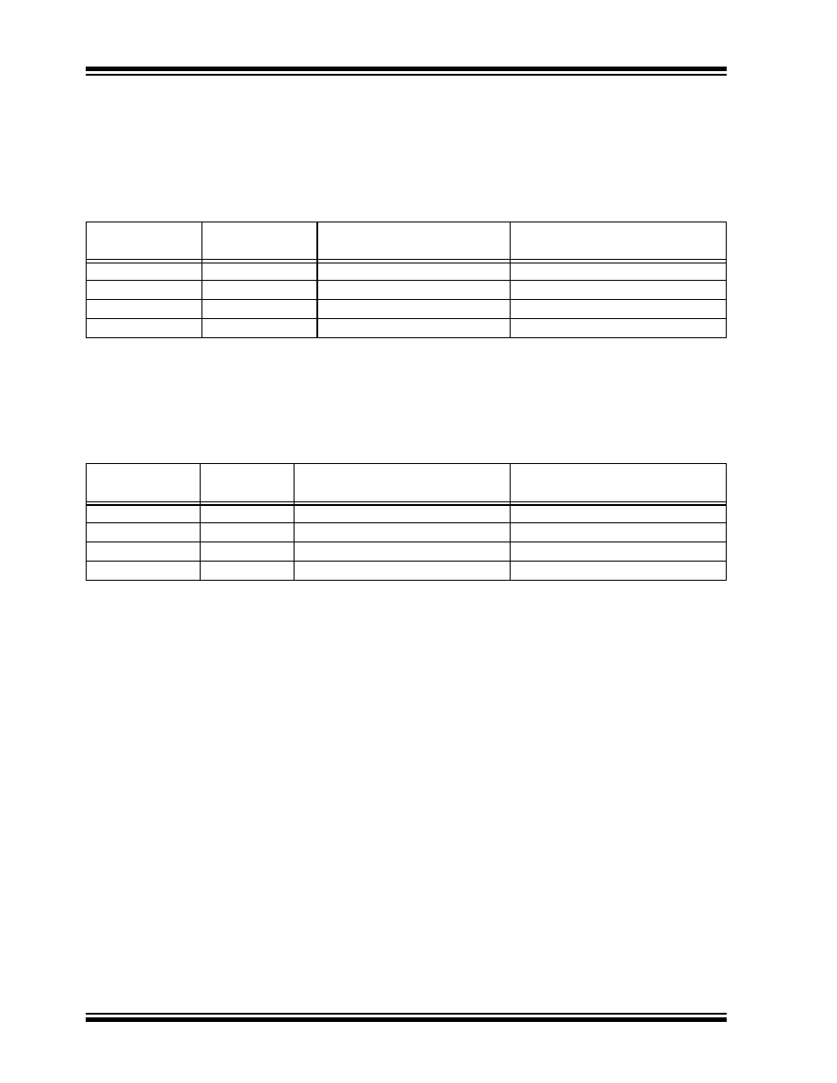
TABLE 2-1:
PIN DESCRIPTIONS
The HCS361 will wake-up upon detecting a button
press and delay approximately 10 ms for button
debounce (Figure 2-2). The synchronization counter,
discrimination value and button information will be
encrypted to form the hopping code. The hopping code
portion will change every transmission, even if the
same button is pushed again. A code word that has
been transmitted will not repeat for more than 64K
transmissions. This provides more than 18 years of use
before a code is repeated; based on 10 operations per
day. Overflow information sent from the encoder can be
used to extend the number of unique transmissions to
more than 192K.
If in the transmit process it is detected that a new but-
ton(s) has been pressed, a RESET will immediately
occur and the current code word will not be completed.
Please note that buttons removed will not have any
effect on the code word unless no buttons remain
pressed; in which case the code word will be completed
and the power-down will occur.
FIGURE 2-2:
ENCODER OPERATION
Name
Pin
Number
Description
S0
1
Switch input 0
S1
2
Switch input 1
S2
3
Switch input 2 / Clock pin when in
Programming mode
S3
4
Switch input 3
V
SS
5
Ground reference
DATA
6
Data output pin /Data I/O pin for
Programming mode
LED
7
Cathode connection for LED
V
DD
8
Positive supply voltage
V
DD
B0
Tx out
S0
S1
S2
S3
LED
V
DD
DATA
V
SS
Two button remote control
B1
V
DD
Tx out
S0
S1
S2
S3
LED
V
DD
DATA
V
SS
Five button remote control (Note
1
)
B4 B3 B2 B1 B0
Note:
Up to 15 functions can be implemented by pressing
more than one button simultaneously or by using a
suitable diode array.
Power-Up
RESET and Debounce Delay
(10 ms)
Sample Inputs
Update Sync Info
Encrypt With
Load Transmit Register
Buttons
Added
?
All
Buttons
Released
?
(A button has been pressed)
Transmit
Stop
No
Yes
No
Yes
Crypt Key
Complete Code
Word Transmission

HCS361
DS40146E-page 6
�
2002 Microchip Technology Inc.
3.0
EEPROM MEMORY
ORGANIZATION
The HCS361 contains 192 bits (12 x 16-bit words) of
EEPROM memory (Table 3-1). This EEPROM array is
used to store the encryption key information,
synchronization value, etc. Further descriptions of the
memory array is given in the following sections.
TABLE 3-1:
EEPROM MEMORY MAP
3.1
KEY_0 - KEY_3 (64-Bit Crypt Key)
The 64-bit crypt key is used to create the encrypted
message transmitted to the receiver. This key is calcu-
lated and programmed during production using a key
generation algorithm. The key generation algorithm
may be different from the K
EE
L
OQ
algorithm. Inputs to
the key generation algorithm are typically the transmit-
ter's serial number and the 64-bit manufacturer's code.
While the key generation algorithm supplied from
Microchip is the typical method used, a user may elect
to create their own method of key generation. This may
be done providing that the decoder is programmed with
the same means of creating the key for
decryption purposes.
3.2
SYNC_A, SYNC_B
(Synchronization Counter)
This is the 16-bit synchronization value that is used to
create the hopping code for transmission. This value is
incremented after every transmission. Separate syn-
chronization counters can be used to stay synchro-
nized with different receivers.
3.3
SEED_0, SEED_1, and SEED_2
(Seed Word)
The three word (48 bits) seed code will be transmitted
when seed transmission is selected. This allows the sys-
tem designer to implement the Secure Learn feature or
use this fixed code word as part of a different key genera-
tion/tracking process or purely as a fixed code transmis-
sion.
3.4
SER_0, SER_1
(Encoder Serial Number)
SER_0 and SER_1 are the lower and upper words of
the device serial number, respectively. There are 32
bits allocated for the Serial Number and a selectable
configuration bit determines whether 32 or 28 bits will
be transmitted. The serial number is meant to be
unique for every transmitter.
WORD
ADDRESS
MNEMONIC
DESCRIPTION
0
KEY_0
64-bit crypt key
(word 0) LSb's
1
KEY_1
64-bit crypt key
(word 1)
2
KEY_2
64-bit crypt key
(word 2)
3
KEY_3
64-bit crypt key
(word 3) MSb's
4
SYNC_A
16-bit synch counter
5
SYNC_B/
SEED_2
16-bit synch counter B
or Seed value (word 2)
6
RESERVED Set to 0000H
7
SEED_0
Seed Value
(word 0) LSb's
8
SEED_1
Seed Value
(word 1) MSb's
9
SER_0
Device Serial Number
(word 0) LSb's
10
SER_1
Device Serial Number
(word 1) MSb's
11
CONFIG
Configuration Word
Note:
Since SEED2 and SYNC_B share the
same memory location, Secure Learn and
Independent mode transmission (including
IR mode) are mutually exclusive.
�
2002 Microchip Technology Inc.
DS40146E-page 7
HCS361
3.5
CONFIG
(Configuration Word)
The Configuration Word is a 16-bit word stored in
EEPROM array that is used by the device to store
information used during the encryption process, as well
as the status of option configurations. Further
explanations of each of the bits are described in the
following sections.
TABLE 3-1:
CONFIGURATION WORD
3.5.1
MOD: MODULATION FORMAT
MOD selects between VPWM modulation and PWM
modulation format.
If MOD = 1, VPWM modulation is selected as well as
the following:
1.
Enables the TXWAK bit to select the WAKE-UP
transmission.
2.
Extends the Guard Time.
If MOD = 0, PWM modulation is selected.
3.5.2
BSEL: BAUD RATE SELECT
BSEL selects the baud rate. If BSEL = 1, the baud rate
is nominally 1667 bits per second and with BSEL = 0,
833 bits per second.
3.5.3
TXWAK: BIT FORMAT SELECT OR
WAKE-UP
In PWM mode, this bit selects the bit format.
If TXWAK = 0, the PWM pulse duty cycle is 1/3-2/3.
If TXWAK = 1, the PWM pulse duty cycle is 1/6-2/6.
In VPWM mode, this bit enables the wake-up signal.
If TXWAK = 0, transmissions start normally with the
preamble portion of the code word.
If TXWAK = 1, transmissions start with a Wake-up
sequence followed by a dead time (see Figure 4-2).
The following tables summarize the combined effect of
TXWAK, BSEL and MOD option bits.
TABLE 3-1:
PWM OPTIONS
TABLE 3-2:
VPWM OPTIONS
3.5.4
SPM: SYNC PULSE MODULATION
Select Modulation mode of Sync Pulse. If SPM = 1, the
sync pulse is modulated (Figure 4-1 and Figure 4-2).
3.5.5
OVR: OVERFLOW
The overflow bit is used to extend the number of possi-
ble synchronization values. The synchronization
counter is 16 bits in length, yielding 65,536 values
before the cycle repeats. Under typical use of
10 operations a day, this will provide nearly 18 years of
use before a repeated value will be used. Should the
system designer conclude that is not adequate, then
the overflow bit can be utilized to extend the number of
unique values. This can be done by programming OVR
to 1 at the time of production. The encoder will auto-
matically clear OVR the first time that the transmitted
synchronization value wraps from 0xFFFF to 0x0000.
Once cleared, OVR cannot be set again, thereby creat-
ing a permanent record of the counter overflow. This
prevents fast cycling of 64K counter. If the decoder sys-
tem is programmed to track the overflow bits, then the
effective number of unique synchronization values can
be extended to 128K. If programmed to zero, the sys-
tem will be compatible with old encoder devices.
Bit Number
Symbol
Bit Description
0
BACW
Blank Alternate Code Word
1
BSEL
Baud Rate Selection
2
TXWAK
PWM mode: 1/6, 2/6 or 1/3,
2/3 select
VPWM mode: Wake-up
enable
3
SPM
Sync Pulse Modulation
4
SEED
Seed Transmission enable
5
DELM
Delay mode enable
6
TIMO
Time-out enable
7
IND
Independent mode enable
8 USRA0
User
bit
9
USRA1
User bit
10
USRB0
User bit
11
USRB1
User bit
12
XSER
Extended serial number
enable
13
TMPSD
Temporary seed
transmission enable
14
MOD
Modulation format select
15
OVR
Overflow bit
Note:
The Wake-up sequence is transmitted
before the first code word of each trans-
mission only.
MOD
TXWAK
BSEL
T
E
Duty Cycle
0
0
0
400us
1/3-2/3
0
0
1
200us
1/3-2/3
0
1
0
200us
1/6-2/6
0
1
1
100us
1/6-2/6
MOD
TXWAK
BSEL
T
E
Wake-up
1
0
0
400us
NO
1
0
1
200us
NO
1
1
0
400us
YES
1
1
1
200us
YES

HCS361
DS40146E-page 8
�
2002 Microchip Technology Inc.
3.5.6
BACW: BLANK ALTERNATE CODE
WORD
BACW = 1 selects the encoder to transmit every sec-
ond code word. This can be used to reduce the aver-
age power transmitted over a 100 ms window and
thereby transmit a higher peak power (see
Section 5.2).
3.5.7
XSER: EXTENDED SERIAL
NUMBER
If XSER = 0, the four Most Significant bits of the Serial
Number are substituted by S[3:0] and the code word
format is compatible with the HCS200/300/301.
If XSER = 1, the full 32-bit Serial Number [SER_1,
SER_0] is transmitted.
3.5.8
DISCRIMINATION VALUE
While in other K
EE
L
OQ
encoders its value is user
selectable, the HCS361 uses directly the 8 Least Sig-
nificant bits of the Serial Number as part of the infor-
mation that form the encrypted portion of the
transmission (Figure 3-2).
The discrimination value aids the post-decryption
check on the decoder end. After the receiver has
decrypted a transmission, the discrimination bits are
checked against the encoder Serial Number to verify
that the decryption process was valid.
3.5.9
USRA,B: USER BITS
User bits form part of the discrimination value. The user
bits together with the IND bit can be used to identify the
counter that is used in Independent mode.
FIGURE 3-2:
CODE WORD ORGANIZATION
Note:
Since the button status S[3:0] is used to
detect a Seed transmission, Extended
Serial Number and Secure Learn are
mutually exclusive.
Discrimination Bits
(12 bits)
I
O
U
U
S
S
...
S
N
V
S
S
E
E
...
E
D
R
R
R
R
R
...
R
1
0
7
6
...
0
Fixed Code Portion of Transmission
Encrypted Portion of Transmission
67 bits
of Data
Transmitted
MSB
LSB
CRC
(2-bit)
V
LOW
(1-bit)
Button
Status
(4 bits)
28-bit
Serial Number
Button
Status
(4 bits)
Discrimination
bits
(12 bits)
16-bit
Sync Value
Button Status
(4 bits)
S
S
S
S
2
1
0
3
Fixed Code Portion of Transmission
Encrypted Portion of Transmission
MSB
LSB
CRC
(2-bit)
V
LOW
(1-bit)
32-bit
Extended Serial Number
Button
Status
(4 bits)
Discrimination
bits
(12 bits)
16-bit
Sync Value
XSER=1
XSER=0
�
2002 Microchip Technology Inc.
DS40146E-page 9
HCS361
3.5.10
SEED: ENABLE SEED
TRANSMISSION
If SEED = 0, seed transmission is disabled. The Inde-
pendent Counter mode can only be used with seed
transmission disabled since SEED_2 is shared with the
second synchronization counter.
With SEED = 1, seed transmission is enabled. The
appropriate button code(s) must be activated to trans-
mit the seed information. In this mode, the seed infor-
mation (SEED_0, SEED_1, and SEED_2) and the
upper 12 or 16 bits of the serial number (SER_1)are
transmitted instead of the hop code.
Seed transmission is available for function codes
(Table 3-2) S[3:0] = 1001 and S[3:0] = 0011 (delayed).
This takes place regardless of the setting of the IND bit.
The two seed transmissions are shown in Figure 3-3.
FIGURE 3-3:
Seed Transmission
3.5.11
TMPSD: TEMPORARY SEED
TRANSMISSION
The temporary seed transmission can be used to dis-
able learning after the transmitter has been used for a
programmable number of operations. This feature can
be used to implement very secure systems. After learn-
ing is disabled, the seed information cannot be
accessed even if physical access to the transmitter is
possible. If TMPSD = 1 the seed transmission will be
disabled after a number of code hopping transmis-
sions. The number of transmissions before seed trans-
mission is disabled, can be programmed by setting the
synchronization counter (SYNC_A or SYNC_B) to a
value as shown in Table 3-4.
TABLE 3-4:
SYNCHRONOUS COUNTER
INITIALIZATION VALUES
All examples shown with XSER = 1, SEED = 1
When S[3:0] = 1001, delay is not applicable.
CRC+V
LOW
SER_1
SEED_2
SEED_1
SEED_0
Data transmission direction
For S[3:0] = 0x3 before delay:
16-bit Data Word
16-bit Counter
Encrypt
CRC+V
LOW
SER_1
SER_0
Encrypted Data
For S[3:0] = 0011 after delay (Note 1, Note 2):
CRC+V
LOW
SER_1
SEED_2
SEED_1
SEED_0
Data transmission direction
Data transmission direction
Note 1: For Seed Transmission, SEED_2 is transmitted instead of SER_0.
2: For Seed Transmission, the setting of DELM has no effect.
Synchronous Counter
Values
Number of
Transmissions
0000H
128
0060H
64
0050H
32
0048H
16
HCS361
DS40146E-page 10
�
2002 Microchip Technology Inc.
3.5.12
DELM: DELAY MODE
If DELM = 1, delay transmission is enabled. A delayed
transmission is indicated by inverting the lower nibble
of the discrimination value. The Delay mode is primarily
for compatibility with previous K
EE
L
OQ
devices.
If DELM = 0, delay transmission is disabled (Table 3-
1).
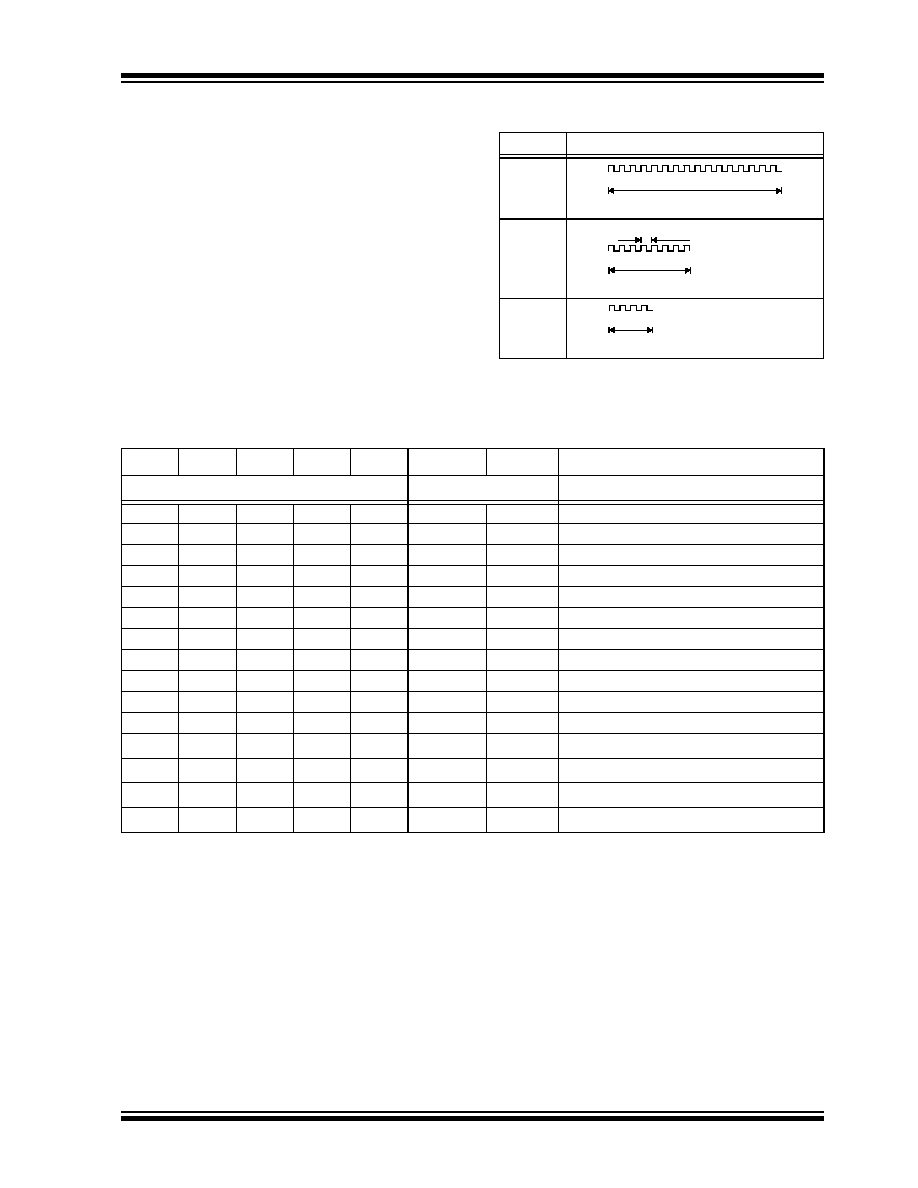
TABLE 3-1:
TYPICAL DELAY TIMES
3.5.13
TIMO: TIME-OUT
OR AUTO-SHUTOFF
If TIMO = 1, the time-out is enabled. Time-out can be
used to terminate accidental continuous transmissions.
When time-out occurs, the PWM output is set low and
the LED is turned off. Current consumption will be
higher than in Standby mode since current will flow
through the activated input resistors. This state can be
exited only after all inputs are taken low. TIMO = 0, will
enable continuous transmission (Table 3-5).
TABLE 3-5:
TYPICAL TIME-OUT TIMES
TXWAK
BSEL
Number of Code Words before
Delay Mode
Time Before Delay Mode (MOD = 0)
0
0
28
2.8s
0
1
56
2.9s
1
0
28
2.6s
1
1
56
2.8s
TXWAK
BSEL
Maximum Number of Code Words
Transmitted
Time Before Time-out (MOD = 0)
0
0
256
25.6s
0
1
512
27.2s
1
0
256
23.8s
1
1
512
25.4s
�
2002 Microchip Technology Inc.
DS40146E-page 11
HCS361
3.5.14
IND: INDEPENDENT MODE
The Independent mode can be used where one
encoder is used to control two receivers. Two counters
(SYNC_A and SYNC_B) are used in Independent
mode. As indicated in Table 3-2, function codes 1 to 7
use SYNC_A and 8 to 15 SYNC_B.
3.5.15
INFRARED MODE
The Independent mode also selects IR mode. In IR
mode function codes 12 to 15 will use counter B. The
PWM output signal is modulated with a 40 kHz carrier
(see Table 3-1). It must be pointed out that the 40 kHz
is derived from the internal clock and will therefore vary
with the same percentage as the baud rate. If IND = 0,
SYNC_A is used for all function codes. If IND = 1, Inde-
pendent mode is enabled and counters for functions
are used according to Table 3-2.
TABLE 3-1:
IR MODULATION
TABLE 3-2:
FUNCTION CODES
Note 1: IR mode
T
E
Basic Pulse
400us
200us
100us
(400
�
s)
(16x)
(200
�
s)
(8x)
Period = 25
�
s
(100
�
s)
(4x)
S3
S2
S1
S0
IND = 0
IND = 1
Comments
Counter
1
0
0
0
1
A
A
2
0
0
1
0
A
A
3
0
0
1
1
A
A
If SEED = 1, transmit seed after delay.
(1)
4
0
1
0
0
A
A
5
0
1
0
1
A
A
6
0
1
1
0
A
A
7
0
1
1
1
A
A
8
1
0
0
0
A
B
9
1
0
0
1
A
B
If SEED = 1, transmit seed immediately.
(1)
10
1
0
1
0
A
B
11
1
0
1
1
A
B
12
1
1
0
0
A
B
(1)
13
1
1
0
1
A
B
(1)
14
1
1
1
0
A
B
(1)
15
1
1
1
1
A
B
(1)
HCS361
DS40146E-page 12
�
2002 Microchip Technology Inc.
4.0
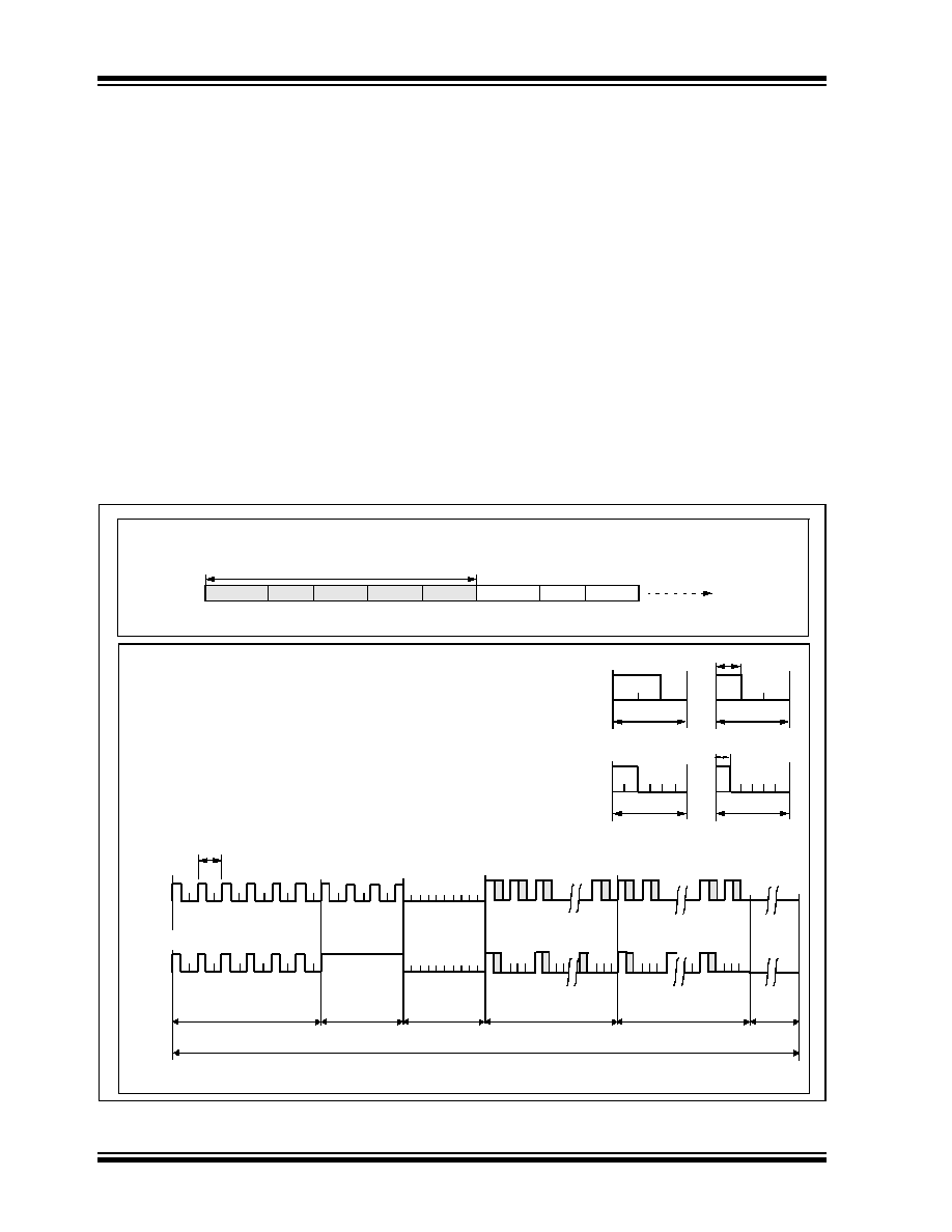
TRANSMITTED WORD
4.1
Transmission Format (PWM)
The HCS361 transmission is made up of several parts
(Figure 4-1 and Figure 4-2). Each transmission is
begun with a preamble and a header, followed by the
encrypted and then the fixed data. The actual data is
67 bits which consists of 32 bits of encrypted data and
35 bits of fixed data. Each transmission is followed by
a guard period before another transmission can begin.
Refer to Table 8-6 and Table 8-6 for transmission tim-
ing specifications. The encrypted portion provides up to
four billion changing code combinations and includes
the function bits (based on which buttons were acti-
vated) along with the synchronization counter value
and discrimination value. The non-encrypted portion is
comprised of the CRC bits, V
LOW
bits, the function bits
and the 28/32-bit serial number. The encrypted and
non-encrypted sections combined increase the number
of combinations to 1.47 x 10
20
.
4.2
Code Word Organization
The HCS361 transmits a 67-bit code word when a but-
ton is pressed. The 67-bit word is constructed from a
Fixed Code portion and an Encrypted Code portion
(Figure 3-2).
The Encrypted Data is generated from 4 function bits,
2 user bits, overflow bit, Independent mode bit, and 8
serial number bits, and the 16-bit synchronization value
(Figure 8-4).
The Non-encrypted Code Data is made up of V
LOW
bit, 2 CRC bits, 4 function bits, and the 28-bit serial
number. If the extended serial number (32 bits) is
selected, the 4 function code bits will not be transmit-
ted.
FIGURE 4-1:
PWM Transmission Format (MOD = 0)
T
BP
=6
X
T
E
Duty Cycle: 1/6-2/6
CODE WORD:
TRANSMISSION SEQUENCE:
Preamble Header Encrypt
Fixed
Guard
1st CODE WORD
Preamble Header Encrypt
(TXWAK=1)
T
BP
LOGIC 0
LOGIC 1
Duty Cycle: 1/3-2/3
(TXWAK=0)
T
BP
=3
X
T
E
LOGIC 0
T
BP
LOGIC 1
T
E
T
E
Code Word
Guard
Time
SPM=1
SPM=0
18xT
E
Preamble
10xT
E
Header
Encrypted Portion
Fixed Code Portion
T
BP
1
6
10
10xT
E
Sync
TXWAK=0
TXWAK=1
33% Duty Cycle
Pulse
�
2002 Microchip Technology Inc.
DS40146E-page 13
HCS361
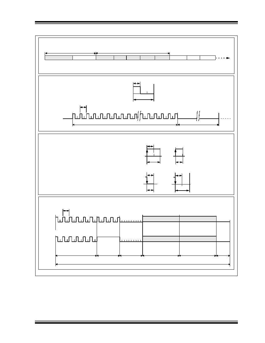
FIGURE 4-2:
VPWM TRANSMISSION FORMAT (MOD = 1)
VPWM BIT ENCODING:
VPWM TRANSMISSION SEQUENCE:
WAKE-UP (TXWAK=1)
Preamble Header Encrypt Fixed
Guard
Dead Time
1st CODE WORD
Preamble Header Encrypt
T
BP
Code Word
Guard
Time
SPM=1
SPM=0
18xT
E
Preamble
10xT
E
Header
Encrypted Portion
Fixed Code Portion
T
BP
1
6
10
LOGIC 0
LOGIC 1
on Transition Low to High
T
BP
LOGIC 0
T
BP
LOGIC 1
T
E
33% Duty Cycle Wake-Up sequence 250xT
E
on Transition High to Low
2
X
T
E
WAKE-UP:
T
E
T
BP
T
E
CODE WORD:
T
BP
1
84
T
BP
T
E
Dead Time 258xT
E
2
X
T
E
10xT
E
Sync
Pulse

HCS361
DS40146E-page 14
�
2002 Microchip Technology Inc.
5.0
SPECIAL FEATURES
5.1
Code Word Completion
Code word completion is an automatic feature that
ensures that the entire code word is transmitted, even
if the button is released before the transmission is com-
plete and that a minimum of two words are completed.
The HCS361 encoder powers itself up when a button is
pushed and powers itself down after the current trans-
mission is finished, if the user has already released the
button. If the button is held down beyond the time for
two transmissions, then multiple transmissions will
result. The HCS361 transmits at least two transmis-
sions before powering down. If another button is acti-
vated during a transmission, the active transmission
will be aborted and the new code will be generated
using the new button information.
5.2
Blank Alternate Code Word
Federal Communications Commission (FCC) part 15
rules specify the limits on fundamental power and
harmonics that can be transmitted. Power is calculated
on the worst case average power transmitted in a 100
ms window. It is therefore advantageous to minimize
the duty cycle of the transmitted word. This can be
achieved by minimizing the duty cycle of the individual
bits and by blanking out consecutive words. Blank
Alternate Code Word (BACW) is used for reducing the
average power of a transmission (Figure 5-1). This is a
selectable feature. Using the BACW allows the user to
transmit a higher amplitude transmission if the
transmission length is shorter. The FCC puts
constraints on the average power that can be
transmitted by a device, and BACW effectively
prevents continuous transmission by only allowing the
transmission of every second word. This reduces the
average power transmitted and hence, assists in FCC
approval of a transmitter device.
5.3
CRC (Cycle Redundancy Check)
Bits
The CRC bits are calculated on the 65 previously trans-
mitted bits. The CRC bits can be used by the receiver
to check the data integrity before processing starts. The
CRC can detect all single bit and 66% of double bit
errors. The CRC is computed as follows:
EQUATION 5-1:
CRC Calculation
and
with
and
Di
n
the nth transmission bit 0 � n � 64
FIGURE 5-1:
BLANK ALTERNATE CODE WORD (BACW)
Note: The CRC may be wrong when the battery
voltage is around either of the V
LOW
trip
points. This may happen because V
LOW
is
sampled twice each transmission, once for
the CRC calculation (PWM is low) and once
when V
LOW
is transmitted (PWM is high).
V
DD
tends to move slightly during a transmis-
sion which could lead to a different value for
V
LOW
being used for the CRC calculation
and the transmission
. Work around: If the CRC calculation is incor-
rect, recalculate for the opposite value of
V
LOW
.
CRC 1
[ ]
n
1
+
CRC 0
[ ]
n
Di
n
=
CRC 0
[ ]
n
1
+
CRC 0
[ ]
n
Di
n
(
)
CRC 1
[ ]
n
=
CRC 1 0
,
[
]
0
0
=
Code Word
BRS = 0
BRS = 1
A
2A
Time
Code Word
Code Word
Code Word
Amplitude
�
2002 Microchip Technology Inc.
DS40146E-page 15
HCS361
5.4
Auto-shutoff
The Auto-shutoff function automatically stops the
device from transmitting if a button inadvertently gets
pressed for a long period of time. This will prevent the
device from draining the battery if a button gets
pressed while the transmitter is in a pocket or purse.
This function can be enabled or disabled and is
selected by setting or clearing the time-out bit
(Section 3.5.13). Setting this bit will enable the function
(turn Auto-shutoff function on) and clearing the bit will
disable the function. Time-out period is approximately
25 seconds.
5.5
V
LOW
: Voltage LOW Indicator
The V
LOW
bit is transmitted with every transmission
(Figure 3-2) and will be transmitted as a one if the
operating voltage has dropped below the low voltage
trip point, typically 3.8V at 25�C. This V
LOW
signal is
transmitted so the receiver can give an indication to the
user that the transmitter battery is low.
5.6
LED Output Operation
During normal transmission the LED output is LOW
while the data is being transmitted and high during the
guard time. Two voltage indications are combined into
one bit: V
LOW
. Table 5-1 indicates the operation value
of V
LOW
while data is being transmitted.
FIGURE 5-2:
V
LOW
Trip Point VS.
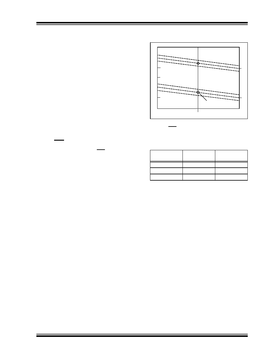
Temperature
If the supply voltage drops below the low voltage trip
point, the LED output will be toggled at approximately
1Hz during the transmission.
TABLE 5-1:
V
LOW
AND LED VS. V
DD
*See also FLASH operating modes.
Approximate
Supply Voltage
Vlow Bit
LED Operation*
Max
3.8V
0
Normal
3.8V
2.2V 1
Flashing
2.2V
Min
0
Normal
3.5
2V
-40
25
85
V
LOW
=0
Nominal Trip Point
3.8V
V
LOW
=1
V
LOW
=0
Nominal Trip
Point
4.5
4
3.5
3
2.5
2
1.5
HCS361
DS40146E-page 16
�
2002 Microchip Technology Inc.
6.0
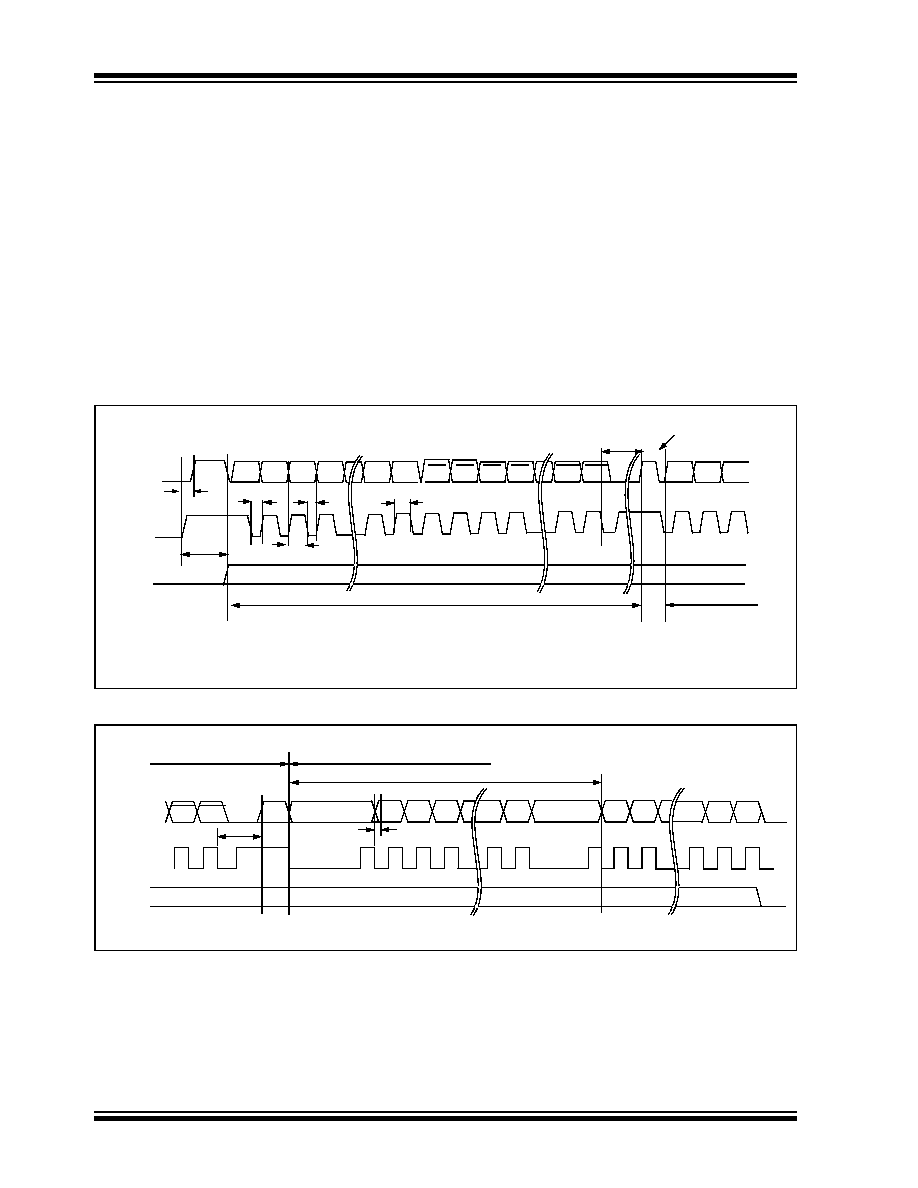
PROGRAMMING THE HCS361
When using the HCS361 in a system, the user will have
to program some parameters into the device including
the serial number and the secret key before it can be
used. The programming cycle allows the user to input
all 192 bits in a serial data stream, which are then
stored internally in EEPROM. Programming will be
initiated by forcing the PWM line high, after the S3 line
has been held high for the appropriate length of time.
S0 should be held low during the entire program cycle.
The S1 line on the HCS361 part needs to be set or
cleared depending on the LS bit of the memory map
(Key 0) before the key is clocked in to the HCS361. S1
must remain at this level for the duration of the pro-
gramming cycle. The device can then be programmed
by clocking in 16 bits at a time, followed by the word's
complement using S3 or S2 as the clock line and PWM
as the data in line. After each 16-bit word is loaded, a
programming delay is required for the internal program
cycle to complete. An Acknowledge bit can be read
back after the programming delay (T
WC
). After the first
word and its complement have been downloaded, an
automatic bulk write is performed. This delay can take
up to Twc. At the end of the programming cycle, the
device can be verified (Figure 6-1) by reading back the
EEPROM. Reading is done by clocking the S3 line and
reading the data bits on PWM. For security reasons, it
is not possible to execute a Verify function without first
programming the EEPROM. A Verify operation can
only be done once, immediately following the Pro-
gram cycle.
FIGURE 6-1:
Programming Waveforms
FIGURE 6-2:
Verify Waveforms
The V
DD
pin must be taken to ground after a program/verify cycle.
DATA
Enter Program
Mode
(Data)
(Clock)
Bit 1
Bit 2
Bit 3
Bit 14 Bit 15
Bit 16 Bit 17
T
1
T
2
Repeat for each word
T
CLKH
T
CLKL
T
WC
T
DS
S2/S3
Data for Word 0 (KEY_0)
Data for Word 1
T
DH
Bit 0
Bit 1
Bit 2
Bit 3
Bit 14 Bit 15
S1
Bit 0
Bit 0 of Word0
Note 1: Unused button inputs to be held to ground during the entire programming sequence.
2: The V
DD
pin must be taken to ground after a Program/Verify cycle.
Acknowledge Pulse
DATA
(Clock)
(Data)
Note: A Verify sequence is performed only once immediately after the Program cycle.
End of Programming Cycle
Beginning of Verify Cycle
Bit 1 Bit 2
Bit 3
Bit 15
Bit 14
Bit 16 Bit 17
Bit190 Bit191
T
WC
Data from Word0
T
DV
S2/S3
Bit 0
Bit191
Bit190
S1
Ack

�
2002 Microchip Technology Inc.
DS40146E-page 17
HCS361
TABLE 6-3:
PROGRAMMING/VERIFY TIMING REQUIREMENTS
Note 1: Typical values - not tested in production.
V
DD
= 5.0V
�
10%
25
�
C
�
5
�
C
Parameter
Symbol
Min.
Max.
Units
Program mode setup time
T
2
0
4.0
ms
Hold time 1
T
1
9.0
--
ms
Program cycle time
T
WC
50
--
ms
Clock low time
T
CLKL
50
--
�
s
Clock high time
T
CLKH
50
--
�
s
Data setup time
T
DS
0
--
�
s
(1)
Data hold time
T
DH
30
--
�
s
(1)
Data out valid time
T
DV
--
30
�
s
(1)
HCS361
DS40146E-page 18
�
2002 Microchip Technology Inc.
7.0
INTEGRATING THE HCS361
INTO A SYSTEM
Use of the HCS361 in a system requires a compatible
decoder. This decoder is typically a microcontroller with
compatible firmware. Microchip will provide (via a
license agreement) firmware routines that accept
transmissions from the HCS361 and decrypt the
hopping code portion of the data stream. These
routines provide system designers the means to
develop their own decoding system.
7.1
Learning a Transmitter to a
Receiver
A transmitter must first be 'learned' by a decoder before
its use is allowed in the system. Several learning strat-
egies are possible, Figure 7-1 details a typical learn
sequence. Core to each, the decoder must minimally
store each learned transmitter's serial number and cur-
rent synchronization counter value in EEPROM. Addi-
tionally, the decoder typically stores each transmitter's
unique crypt key. The maximum number of learned
transmitters will therefore be relative to the available
EEPROM.
A transmitter's serial number is transmitted in the clear
but the synchronization counter only exists in the code
word's encrypted portion. The decoder obtains the
counter value by decrypting using the same key used
to encrypt the information. The K
EE
L
OQ
algorithm is a
symmetrical block cipher so the encryption and decryp-
tion keys are identical and referred to generally as the
crypt key. The encoder receives its crypt key during
manufacturing. The decoder is programmed with the
ability to generate a crypt key as well as all but one
required input to the key generation routine; typically
the transmitter's serial number.
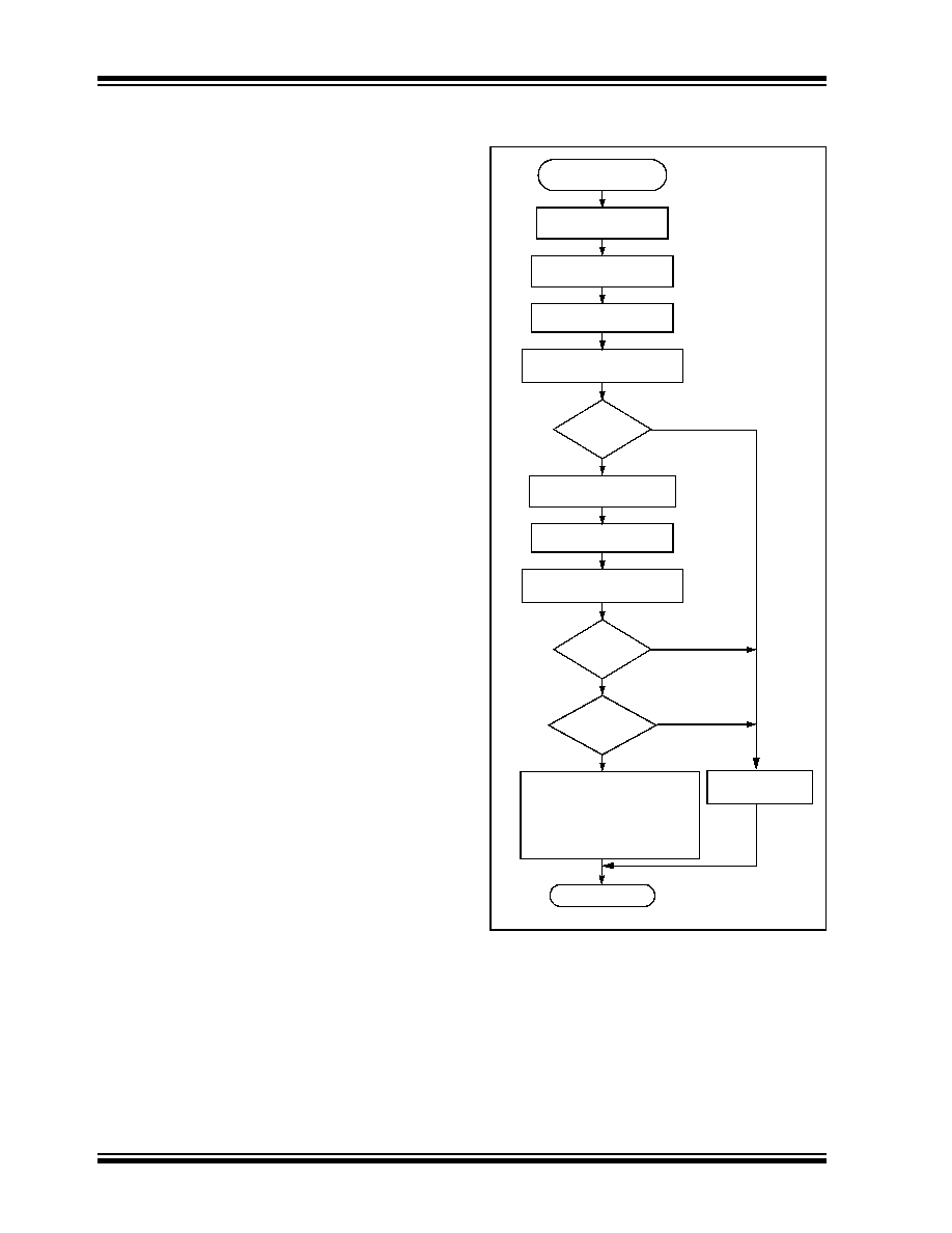
Figure 7-1 summarizes a typical learn sequence. The
decoder receives and authenticates a first transmis-
sion; first button press. Authentication involves gener-
ating the appropriate crypt key, decrypting, validating
the correct key usage via the discrimination bits and
buffering the counter value. A second transmission is
received and authenticated. A final check verifies the
counter values were sequential; consecutive button
presses. If the learn sequence is successfully com-
plete, the decoder stores the learned transmitter's
serial number, current synchronization counter value
and appropriate crypt key. From now on the crypt key
will be retrieved from EEPROM during normal opera-
tion instead of recalculating it for each transmission
received.
Certain learning strategies have been patented and
care must be taken not to infringe.
FIGURE 7-1:
TYPICAL LEARN
SEQUENCE
Enter Learn
Mode
Wait for Reception
of a Valid Code
Generate Key
from Serial Number
Use Generated Key
to Decrypt
Compare Discrimination
Value with Fixed Value
Equal
Wait for Reception
of Second Valid Code
Compare Discrimination
Value with Fixed Value
Use Generated Key
to Decrypt
Equal
Counters
Encryption key
Serial number
Synchronization counter
Sequential
?
?
?
Exit
Learn successful Store:
Learn
Unsuccessful
No
No
No
Yes
Yes
Yes
�
2002 Microchip Technology Inc.
DS40146E-page 19
HCS361
7.2
Decoder Operation
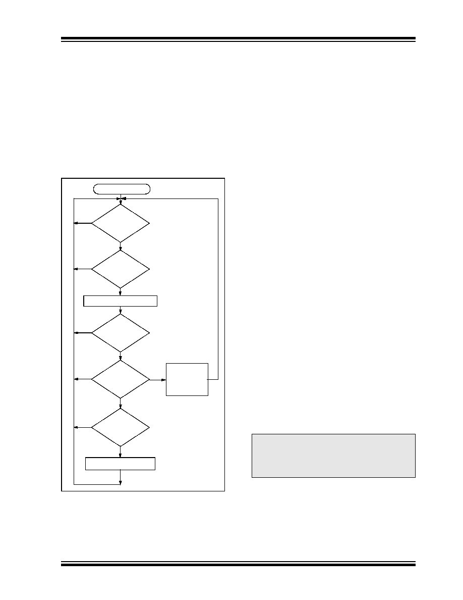
Figure 7-2 summarizes normal decoder operation. The
decoder waits until a transmission is received. The
received serial number is compared to the EEPROM
table of learned transmitters to first determine if this
transmitter's use is allowed in the system. If from a
learned transmitter, the transmission is decrypted
using the stored crypt key and authenticated via the
discrimination bits for appropriate crypt key usage. If
the decryption was valid the synchronization value is
evaluated.
FIGURE 7-2:
TYPICAL DECODER
OPERATION
7.3
Synchronization with Decoder
(Evaluating the Counter)
The K
EE
L
OQ
technology patent scope includes a
sophisticated synchronization technique that does not
require the calculation and storage of future codes. The
technique securely blocks invalid transmissions while
providing transparent resynchronization to transmitters
inadvertently activated away from the receiver.
Figure 7-3 shows a 3-partition, rotating synchronization
window. The size of each window is optional but the
technique is fundamental. Each time a transmission is
authenticated, the intended function is executed and
the transmission's synchronization counter value is
stored in EEPROM. From the currently stored counter
value there is an initial "Single Operation" forward win-
dow of 16 codes. If the difference between a received
synchronization counter and the last stored counter is
within 16, the intended function will be executed on the
single button press and the new synchronization
counter will be stored. Storing the new synchronization
counter value effectively rotates the entire synchroniza-
tion window.
A "Double Operation" (resynchronization) window fur-
ther exists from the Single Operation window up to 32K
codes forward of the currently stored counter value. It
is referred to as "Double Operation" because a trans-
mission with synchronization counter value in this win-
dow will require an additional, sequential counter
transmission prior to executing the intended function.
Upon receiving the sequential transmission the
decoder executes the intended function and stores the
synchronization counter value. This resynchronization
occurs transparently to the user as it is human nature
to press the button a second time if the first was unsuc-
cessful.
The third window is a "Blocked Window" ranging from
the double operation window to the currently stored
synchronization counter value. Any transmission with
synchronization counter value within this window will
be ignored. This window excludes previously used,
perhaps code-grabbed transmissions from accessing
the system.
?
Transmission
Received
Does
Serial Number
Match
?
Decrypt Transmission
Is
Decryption
Valid
?
Is
Counter
Within 16
?
Is
Counter
Within 32K
?
Update
Counter
Execute
Command
Save Counter
in Temp Location
Start
No
No
No
No
Yes
Yes
Yes
Yes
Yes
No
and
No
Note:
The synchronization method described in
this section is only a typical implementation
and because it is usually implemented in
firmware, it can be altered to fit the needs
of a particular system.

HCS361
DS40146E-page 20
�
2002 Microchip Technology Inc.
FIGURE 7-3:
SYNCHRONIZATION WINDOW
Blocked
Entire Window
rotates to eliminate
use of previously
used codes
Single Operation
Window
Window
(32K Codes)
(16 Codes)
Double Operation
(resynchronization)
Window
(32K Codes)
Stored
Synchronization
Counter Value

�
2002 Microchip Technology Inc.
DS40146E-page 21
HCS361
8.0
ELECTRICAL CHARACTERISTICS
TABLE 8-1:
ABSOLUTE MAXIMUM RATINGS
TABLE 8-2:
DC CHARACTERISTICS
Symbol
Item
Rating
Units
V
DD
Supply voltage
-0.3 to 6.9
V
V
IN
Input voltage
-0.3 to V
DD
+ 0.3
V
V
OUT
Output voltage
-0.3 to V
DD
+ 0.3
V
I
OUT
Max output current
25
mA
T
STG
Storage temperature
-55 to +125
�C (Note)
T
LSOL
Lead soldering temp
300
�C (Note)
V
ESD
ESD rating
4000
V
Note:
Stresses above those listed under "ABSOLUTE MAXIMUM RATINGS" may cause permanent damage to the
device.
Commercial
(C): Tamb = 0
�
C to +70
�
C
Industrial
(I): Tamb = -40
�
C to +85
�
C
2.0V < V
DD
< 3.3
3.0 < V
DD
< 6.6
Parameter
Sym.
Min
Typ
1
Max
Min
Typ
1
Max
Unit
Conditions
Operating current (avg)
I
CC
0.3
1.2
0.7
1.6
mA V
DD
= 3.3V
V
DD
= 6.6V
Standby current
I
CCS
0.1
1.0
0.1
1.0
�
A
Auto-shutoff current
2,3
I
CCS
40
75
160
350
�
A
High level Input voltage
V
IH
0.55V
DD
V
DD
+0.3 0.55V
DD
V
DD
+0.3 V
Low level input voltage
V
IL
-0.3
0.15V
DD
-0.3
0.15V
DD
V
High level output voltage
V
OH
0.7V
DD
0.7V
DD
V
I
OH
= -1.0 mA, V
DD
= 2.0V
I
OH
= -2.0 mA, V
DD
= 6.6V
Low level output voltage
V
OL
0.08V
DD
0.08V
DD
V
I
OL
= 1.0 mA, V
DD
= 2.0V
I
OL
= 2.0 mA, V
DD
= 6.6V
LED sink current
I
LED
0.15
1.0
4.0
0.15
1.0
4.0
mA V
LED
4
= 1.5V, V
DD
= 6.6V
Pull-Down
Resistance; S0-S3
R
S
0-3
40
60
80
40
60
80
K
V
DD
= 4.0V
Pull-Down
Resistance; PWM
R
PWM
80
120
160
80
120
160
K
V
DD
= 4.0V
Note 1: Typical values are at 25
�
C.
2: Auto-shutoff current specification does not include the current through the input pull-down resistors.
3: Auto-shutoff current is periodically sampled and not 100% tested
4: V
LED
is the voltage between the V
DD
pin and the LED pin.
HCS361
DS40146E-page 22
�
2002 Microchip Technology Inc.
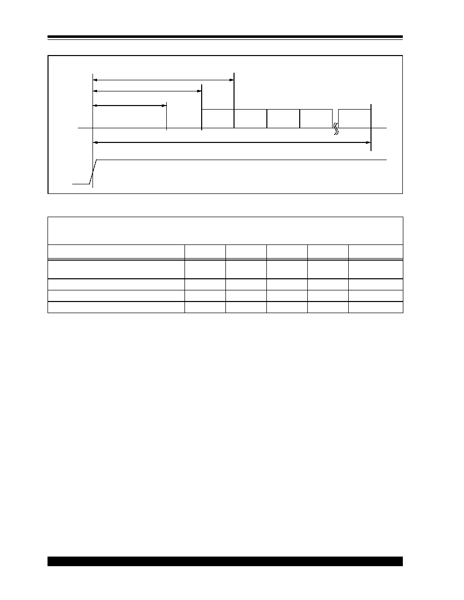
FIGURE 8-1:
POWER-UP AND TRANSMIT TIMING
TABLE 8-3:
POWER-UP AND TRANSMIT TIMING REQUIREMENTS
V
DD
= +2.0 to 6.6V
Commercial
(C): Tamb = 0
�
C to +70
�
C
Industrial
(I): Tamb = -40
�
C to +85
�
C
Parameter
Symbol
Min
Max
Unit
Remarks
Time to second button press
T
BP
10 + Code
Word Time
26 + Code
Word Time
ms
(Note 1)
Transmit delay from button detect
T
TD
4.5
26
ms
(Note 2)
Debounce delay
T
DB
4
13
ms
Auto-shutoff time-out period
T
TO
15
35
s
(Note 3)
Note 1: T
BP
is the time in which a second button can be pressed without completion of the first code word and the
intention was to press the combination of buttons.
2: Transmit delay maximum value if the previous transmission was successfully transmitted.
3: The Auto-shutoff time-out period is not tested.
Button Press
Sn
Detect
T
DB
Output
T
TD
Multiple Code Word Transmission
T
TO
Code
Word
1
Code
Word
2
Code
Word
3
Code
Word
n
T
BP
Code
Word
4
PWM
Input
Button
�
2002 Microchip Technology Inc.
DS40146E-page 23
HCS361
FIGURE 8-2:
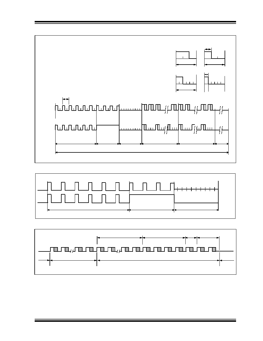
PWM FORMAT SUMMARY (MOD = 0)
FIGURE 8-3:
PWM PREAMBLE/HEADER FORMAT (MOD=0)
FIGURE 8-4:
PWM DATA FORMAT (MOD=0)
T
BP
Code Word
Guard
Time
Duty Cycle: 1/6-2/6
SPM=1
SPM=0
18xT
E
Preamble
10xT
E
Header
Encrypted Portion
Fixed Code Portion
T
BP
CODE WORD:
1
6
10
(TXWAK=1)
T
BP
LOGIC 0
LOGIC 1
Duty Cycle: 1/3-2/3
(TXWAK=0)
T
BP
=3
X
T
E
LOGIC 0
T
BP
LOGIC 1
T
E
T
E
TXWAK=0
TXWAK=1
33% Duty Cycle
10xT
E
Sync
Pulse
SPM = 0
SPM = 1
10xT
E
Header
28xT
E
Preamble
10xT
E
Sync Pulse
Bit 0
Bit 1
Header
Bit 30 Bit 31 Bit 32 Bit 33
Bit 58 Bit 59
Fixed Portion of Transmission
Encrypted Portion
Guard
LSB
LSB
MSB
MSB
S3
S0
S1
S2
V
LOW
CRC0 CRC1
Time
Serial Number
Function Code
Status
Bit 60 Bit 61 Bit 62 Bit 63 Bit 64 Bit 65
CRC
Bit 66
of Transmission
HCS361
DS40146E-page 24
�
2002 Microchip Technology Inc.
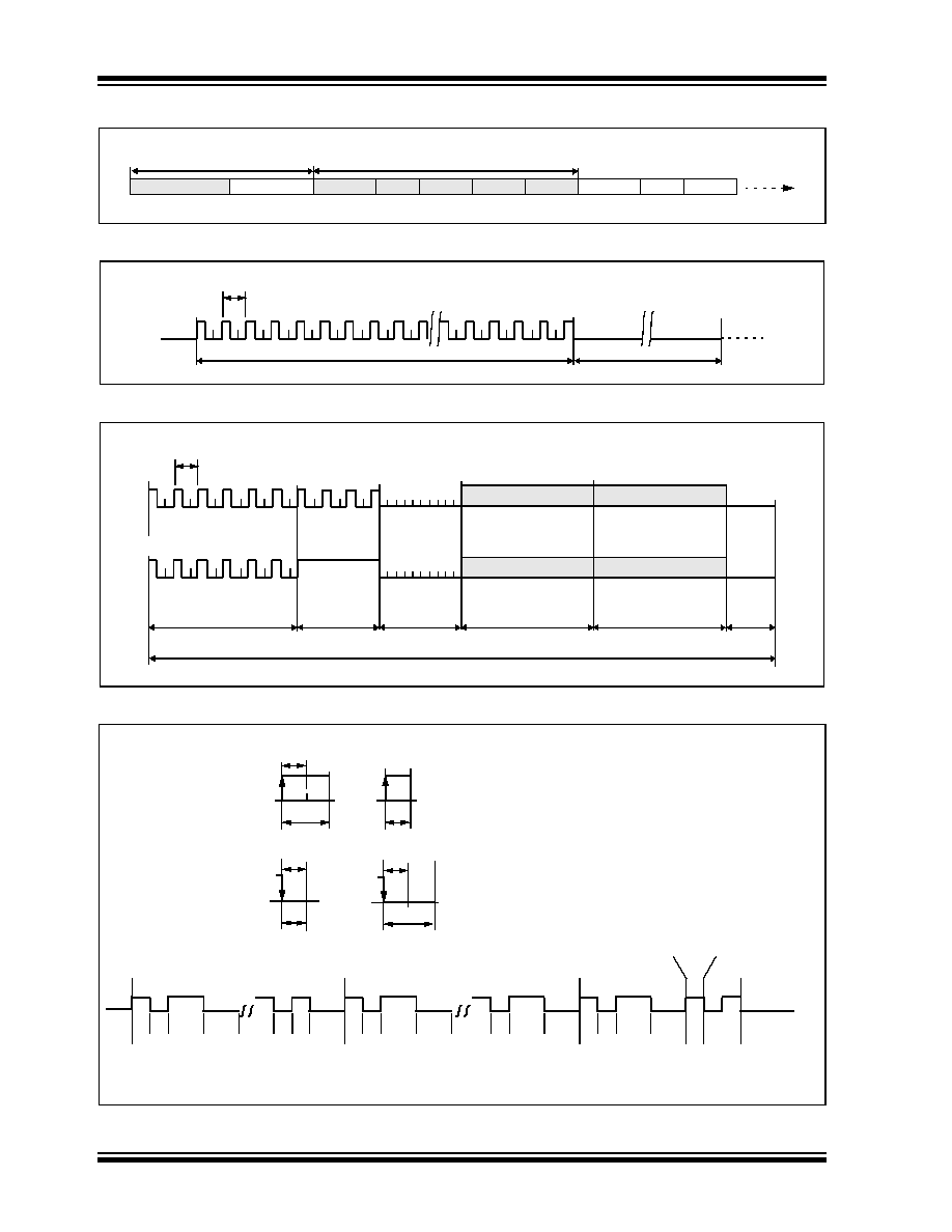
FIGURE 8-5:
VPWM FORMAT SUMMARY (MOD = 1)
FIGURE 8-6:
VPWM WAKE-UP FORMAT (MOD=1)
FIGURE 8-7:
VPWM PREAMBLE/HEADER FORMAT (MOD=1)
FIGURE 8-8:
VPWM DATA WORD FORMAT (MOD=1)
WAKE-UP (TXWAK=1)
Preamble Sync
Encrypt
Fixed
Guard
Dead Time
1st CODE WORD
Preamble Sync Encrypt
33% Duty Cycle Wake-Up sequence 250xT
E
T
BP
1
84
Dead Time 258xT
E
Code Word
Guard
Time
SPM=1
SPM=0
18xT
E
Preamble
10xT
E
Header
Encrypted Portion
Fixed Code Portion
T
BP
1
6
10
10xT
E
Sync
Pulse
1 0
0
1
0 1
2
3
1 0 1
1
28 29 30 31
1 0
0
1
32 33
34
35
1 0
0
1
56 57
58
59
1 0
0
1
60 61
62
63
1 0
64 65
1
66
Encrypted Data
Serial Number
Function Code
V
LOW
CRC
Note:
The bit values are only shown as an example.
Bit
T
BP
LOGIC 0
LOGIC 1
on Transition Low to High
T
BP
LOGIC 0
T
BP
LOGIC 1
T
E
on Transition High to Low
2
X
T
E
T
E
T
BP
T
E

�
2002 Microchip Technology Inc.
DS40146E-page 25
HCS361
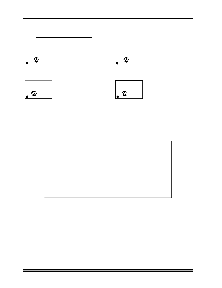
FIGURE 8-9:
HCS361 NORMALIZED TE VS. TEMP
0.8
1.7
1.6
1.5
1.4
1.3
1.2
1.1
1.0
0.9
0.7
0.6
T
E
Min.
T
E
Max.
V
DD
LEGEND
= 2.0V
= 3.0V
= 6.0V
Typical
T
E
Temperature �C
-50 -40 -30 -20 -10 0
10 20 30 40 50 60 70 80 90

HCS361
DS40146E-page 26
�
2002 Microchip Technology Inc.
TABLE 8-4:
TIMING PARAMETERS: PWM MODE (TXWAK=0)
TABLE 8-5:
TIMING PARAMETERS: PWM MODE (TXWAK=1)
V
DD
= +2.0 to 6.6V
Commercial (C):Tamb = 0
�
C to +70
�
C
Industrial
(I):Tamb = -40
�
C to +85
�
C
Code Words Transmitted
BSEL = 0
BSEL = 1
Symbol
Characteristic
Min
Typ.
Max.
Min.
Typ.
Max.
Units
T
E
Basic pulse element
260
400
620
130
200
310
�
s
T
BP
PWM bit pulse width
3
3
T
E
T
P
Preamble duration
28
28
T
E
T
S
Sync Pulse duration
10
10
T
E
T
H
Header duration
10
10
T
E
T
HOP
Hopping code duration
96
96
T
E
T
FIX
Fixed code duration
105
105
T
E
T
G
Guard Time
18
34
T
E
Total Transmit Time
267
283
T
E
Total Transmit Time
69.4
106.8
165.5
36.7
56.6
87.7
ms
PWM data rate
1282
833
538
2564
1667
1075
bps
Note:
The timing parameters are not tested but derived from the oscillator clock.
V
DD
= +2.0 to 6.6V
Commercial (C):Tamb = 0
�
C to +70
�
C
Industrial
(I):Tamb = -40
�
C to +85
�
C
Code Words Transmitted
BSEL = 0
BSEL = 1
Symbol
Characteristic
Min
Typ.
Max.
Min.
Typ.
Max.
Units
T
E
Basic pulse element
130
200
310
65
100
155
�
s
T
BP
PWM bit pulse width
6
6
T
E
T
P
Preamble duration
28
28
T
E
T
S
Sync Pulse duration
10
10
T
E
T
H
Header duration
10
10
T
E
T
HOP
Hopping code duration
192
192
T
E
T
FIX
Fixed code duration
210
210
T
E
T
G
Guard Time
34
66
T
E
Total Transmit Time
484
516
T
E
Total Transmit Time
62.9
96.8
150.0
33.5
51.6
79.9
ms
PWM data rate
1282
833
538
2564
1667
1075
bps
Note:
The timing parameters are not tested but derived from the oscillator clock.

�
2002 Microchip Technology Inc.
DS40146E-page 27
HCS361
TABLE 8-6:
TIMING PARAMETERS: VPWM MODE (BSEL=0)
TABLE 8-7:
TIMING PARAMETERS: VPWM MODE (BSEL=1)
V
DD
= +2.0 to 6.6V
Commercial
(C): Tamb = 0
�
C to +70
�
C
Industrial
(I): Tamb = -40
�
C to +85
�
C
Code Words Transmitted
Shortest
Longest
Symbol
Characteristic
Min
Typ.
Max.
Min.
Typ.
Max.
Units
T
E
Basic pulse element
260
400
620
260
400
620
�
s
T
P
Preamble duration
28
28
T
E
T
S
Sync Pulse duration
10
10
T
E
T
H
Header duration
10
10
T
E
T
HOP
Hopping code duration
32
64
T
E
T
FIX
Fixed code duration
35
70
T
E
T
G
Guard Time
114
114
T
E
Total Transmit Time
229
296
T
E
Total Transmit Time
59.5
91.6
141.9
76.9
118.4
183.5
ms
VPWM data rate
3846
2500
1613
3846
2500
1613
bps
Note:
The timing parameters are not tested but derived from the oscillator clock.
V
DD
= +2.0 to 6.6V
Commercial
(C): Tamb = 0
�
C to +70
�
C
Industrial
(I): Tamb = -40
�
C to +85
�
C
Code Words Transmitted
Shortest
Longest
Symbol
Characteristic
Min
Typ.
Max.
Min.
Typ.
Max.
Units
T
E
Basic pulse element
130
200
310
130
200
310
�
s
T
P
Preamble duration
28
28
T
E
T
S
Sync Pulse duration
10
10
T
E
T
H
Header duration
10
10
T
E
T
HOP
Hopping code duration
32
64
T
E
T
FIX
Fixed code duration
35
70
T
E
T
G
Guard Time
226
226
T
E
Total Transmit Time
341
408
T
E
Total Transmit Time
44.3
68.2
105.7
53.0
81.6
126.4
ms
VPWM data rate
7692
5000
3226
7692
5000
3226
bps
Note:
The timing parameters are not tested but derived from the oscillator clock.
HCS361
DS40146E-page 28
�
2002 Microchip Technology Inc.
9.0
PACKAGING INFORMATION
9.1
Package Marking Information
8-Lead PDIP (300 mil)
Example
8-Lead SOIC (150 mil)
Example
XXXXXXXX
XXXXXNNN
YYWW
HCS361
XXXXXNNN
0025
XXXXXXX
XXXYYWW
NNN
HCS361
XXX0025
NNN
Legend: XX...X
Customer specific information*
Y
Year code (last digit of calendar year)
YY
Year code (last 2 digits of calendar year)
WW
Week code (week of January 1 is week `01')
NNN
Alphanumeric traceability code
Note:
In the event the full Microchip part number cannot be marked on one line, it will
be carried over to the next line thus limiting the number of available characters
for customer specific information.
*
Standard PICmicro device marking consists of Microchip part number, year code, week code, and
traceability code. For PICmicro device marking beyond this, certain price adders apply. Please check
with your Microchip Sales Office. For QTP devices, any special marking adders are included in QTP
price.
�
2002 Microchip Technology Inc.
DS40146E-page 29
HCS361
9.2
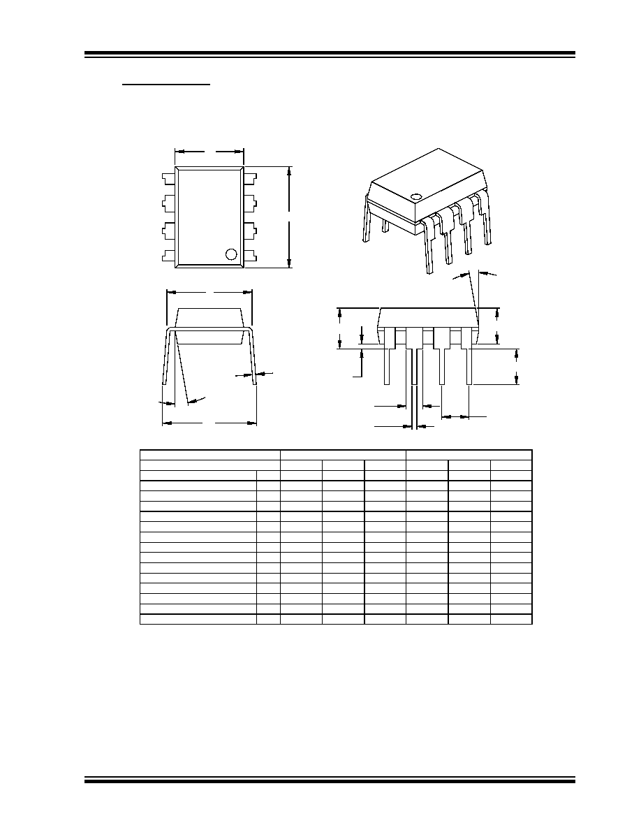
Package Details
8-Lead Plastic Dual In-line (P) - 300 mil (PDIP)
B1
B
A1
A
L
A2
p
E
eB
c
E1
n
D
1
2
Units
INCHES*
MILLIMETERS
Dimension Limits
MIN
NOM
MAX
MIN
NOM
MAX
Number of Pins
n
8
8
Pitch
p
.100
2.54
Top to Seating Plane
A
.140
.155
.170
3.56
3.94
4.32
Molded Package Thickness
A2
.115
.130
.145
2.92
3.30
3.68
Base to Seating Plane
A1
.015
0.38
Shoulder to Shoulder Width
E
.300
.313
.325
7.62
7.94
8.26
Molded Package Width
E1
.240
.250
.260
6.10
6.35
6.60
Overall Length
D
.360
.373
.385
9.14
9.46
9.78
Tip to Seating Plane
L
.125
.130
.135
3.18
3.30
3.43
Lead Thickness
c
.008
.012
.015
0.20
0.29
0.38
Upper Lead Width
B1
.045
.058
.070
1.14
1.46
1.78
Lower Lead Width
B
.014
.018
.022
0.36
0.46
0.56
Overall Row Spacing
�
eB
.310
.370
.430
7.87
9.40
10.92
Mold Draft Angle Top
5
10
15
5
10
15
Mold Draft Angle Bottom
5
10
15
5
10
15
* Controlling Parameter
Notes:
Dimensions D and E1 do not include mold flash or protrusions. Mold flash or protrusions shall not exceed
JEDEC Equivalent: MS-001
Drawing No. C04-018
.010" (0.254mm) per side.
� Significant Characteristic

HCS361
DS40146E-page 30
�
2002 Microchip Technology Inc.
8-Lead Plastic Small Outline (SN) - Narrow, 150 mil (SOIC)
Foot Angle
0
4
8
0
4
8
15
12
0
15
12
0
Mold Draft Angle Bottom
15
12
0
15
12
0
Mold Draft Angle Top
0.51
0.42
0.33
.020
.017
.013
B
Lead Width
0.25
0.23
0.20
.010
.009
.008
c
Lead Thickness
0.76
0.62
0.48
.030
.025
.019
L
Foot Length
0.51
0.38
0.25
.020
.015
.010
h
Chamfer Distance
5.00
4.90
4.80
.197
.193
.189
D
Overall Length
3.99
3.91
3.71
.157
.154
.146
E1
Molded Package Width
6.20
6.02
5.79
.244
.237
.228
E
Overall Width
0.25
0.18
0.10
.010
.007
.004
A1
Standoff
�
1.55
1.42
1.32
.061
.056
.052
A2
Molded Package Thickness
1.75
1.55
1.35
.069
.061
.053
A
Overall Height
1.27
.050
p
Pitch
8
8
n
Number of Pins
MAX
NOM
MIN
MAX
NOM
MIN
Dimension Limits
MILLIMETERS
INCHES*
Units
2
1
D
n
p
B
E
E1
h
L
c
45
�
A2
A
A1
* Controlling Parameter
Notes:
Dimensions D and E1 do not include mold flash or protrusions. Mold flash or protrusions shall not exceed
.010" (0.254mm) per side.
JEDEC Equivalent: MS-012
Drawing No. C04-057
� Significant Characteristic

�
2002 Microchip Technology Inc.
DS40146E-page 31
HCS361
ON-LINE SUPPORT
Microchip provides on-line support on the Microchip
World Wide Web (WWW) site.
The web site is used by Microchip as a means to make
files and information easily available to customers. To
view the site, the user must have access to the Internet
and a web browser, such as Netscape or Microsoft
Explorer. Files are also available for FTP download
from our FTP site.
Connecting to the Microchip Internet Web Site
The Microchip web site is available by using your
favorite Internet browser to attach to:
www.microchip.com
The file transfer site is available by using an FTP ser-
vice to connect to:
ftp://ftp.microchip.com
The web site and file transfer site provide a variety of
services. Users may download files for the latest
Development Tools, Data Sheets, Application Notes,
User's Guides, Articles and Sample Programs. A vari-
ety of Microchip specific business information is also
available, including listings of Microchip sales offices,
distributors and factory representatives. Other data
available for consideration is:
� Latest Microchip Press Releases
� Technical Support Section with Frequently Asked
Questions
� Design Tips
� Device Errata
� Job Postings
� Microchip Consultant Program Member Listing
� Links to other useful web sites related to
Microchip Products
� Conferences for products, Development Systems,
technical information and more
� Listing of seminars and events
Systems Information and Upgrade Hot Line
The Systems Information and Upgrade Line provides
system users a listing of the latest versions of all of
Microchip's development systems software products.
Plus, this line provides information on how customers
can receive any currently available upgrade kits.The
Hot Line Numbers are:
1-800-755-2345 for U.S. and most of Canada, and
1-480-792-7302 for the rest of the world.

HCS361
DS40146E-page 32
�
2002 Microchip Technology Inc.
READER RESPONSE
It is our intention to provide you with the best documentation possible to ensure successful use of your Microchip prod-
uct. If you wish to provide your comments on organization, clarity, subject matter, and ways in which our documentation
can better serve you, please FAX your comments to the Technical Publications Manager at (480) 792-4150.
Please list the following information, and use this outline to provide us with your comments about this Data Sheet.
To:
Technical Publications Manager
RE:
Reader Response
Total Pages Sent
From: Name
Company
Address
City / State / ZIP / Country
Telephone: (_______) _________ - _________
Application (optional):
Would you like a reply? Y N
Device:
Literature Number:
Questions:
FAX: (______) _________ - _________
DS40146E
HCS361
1.
What are the best features of this document?
2.
How does this document meet your hardware and software development needs?
3.
Do you find the organization of this data sheet easy to follow? If not, why?
4.
What additions to the data sheet do you think would enhance the structure and subject?
5.
What deletions from the data sheet could be made without affecting the overall usefulness?
6.
Is there any incorrect or misleading information (what and where)?
7.
How would you improve this document?
8.
How would you improve our software, systems, and silicon products?

�
2002 Microchip Technology Inc.
DS40146E-page 33
HCS361
HCS361 PRODUCT IDENTIFICATION SYSTEM
To order or obtain information, e.g., on pricing or delivery, refer to the factory or the listed sales office.
Sales and Support
Package:
P = Plastic DIP (300 mil Body), 8-lead
SN = Plastic SOIC (150 mil Body), 8-lead
Temperature
Blank = 0�C to +70�C
Range:
I
= �40�C to +85�C
Device:
HCS361
Code Hopping Encoder
HCS361T
Code Hopping Encoder (Tape and Reel)
HCS361
--
/P
Data Sheets
Products supported by a preliminary Data Sheet may have an errata sheet describing minor operational differences and recom-
mended workarounds. To determine if an errata sheet exists for a particular device, please contact one of the following:
1.
Your local Microchip sales office
2.
The Microchip Corporate Literature Center U.S. FAX: (480) 792-7277
3.
The Microchip Worldwide Site (www.microchip.com)
Please specify which device, revision of silicon and Data Sheet (include Literature #) you are using.
New Customer Notification System
Register on our web site (www.microchip.com/cn) to receive the most current information on our products.

HCS361
DS40146E-page 34
�
2002 Microchip Technology Inc.
NOTES:

�
2002 Microchip Technology Inc.
DS40146E - page 35
Information contained in this publication regarding device
applications and the like is intended through suggestion only
and may be superseded by updates. It is your responsibility to
ensure that your application meets with your specifications.
No representation or warranty is given and no liability is
assumed by Microchip Technology Incorporated with respect
to the accuracy or use of such information, or infringement of
patents or other intellectual property rights arising from such
use or otherwise. Use of Microchip's products as critical com-
ponents in life support systems is not authorized except with
express written approval by Microchip. No licenses are con-
veyed, implicitly or otherwise, under any intellectual property
rights.
Trademarks
The Microchip name and logo, the Microchip logo, FilterLab,
K
EE
L
OQ
, MPLAB, PIC, PICmicro, PICMASTER, PICSTART,
PRO MATE, SEEVAL and The Embedded Control Solutions
Company are registered trademarks of Microchip Technology
Incorporated in the U.S.A. and other countries.
dsPIC, ECONOMONITOR, FanSense, FlexROM, fuzzyLAB,
In-Circuit Serial Programming, ICSP, ICEPIC, microID,
microPort, Migratable Memory, MPASM, MPLIB, MPLINK,
MPSIM, MXDEV, PICC, PICDEM, PICDEM.net, rfPIC, Select
Mode and Total Endurance are trademarks of Microchip
Technology Incorporated in the U.S.A.
Serialized Quick Turn Programming (SQTP) is a service mark
of Microchip Technology Incorporated in the U.S.A.
All other trademarks mentioned herein are property of their
respective companies.
� 2002, Microchip Technology Incorporated, Printed in the
U.S.A., All Rights Reserved.
Printed on recycled paper.
Microchip received QS-9000 quality system
certification for its worldwide headquarters,
design and wafer fabrication facilities in
Chandler and Tempe, Arizona in July 1999. The
Company's quality system processes and
procedures are QS-9000 compliant for its
PICmicro
�
8-bit MCUs, K
EE
L
OQ
�
code hopping
devices, Serial EEPROMs and microperipheral
products. In addition, Microchip's quality
system for the design and manufacture of
development systems is ISO 9001 certified.
Microchip's Secure Data Products are covered by some or all of the following patents:
Code hopping encoder patents issued in Europe, U.S.A., and R.S.A. -- U.S.A.: 5,517,187; Europe: 0459781; R.S.A.: ZA93/4726
Secure learning patents issued in the U.S.A. and R.S.A. -- U.S.A.: 5,686,904; R.S.A.: 95/5429

DS40146E-page 36
�
2002 Microchip Technology Inc.
AMERICAS
Corporate Office
2355 West Chandler Blvd.
Chandler, AZ 85224-6199
Tel: 480-792-7200 Fax: 480-792-7277
Technical Support: 480-792-7627
Web Address: http://www.microchip.com
Rocky Mountain
2355 West Chandler Blvd.
Chandler, AZ 85224-6199
Tel: 480-792-7966 Fax: 480-792-7456
Atlanta
500 Sugar Mill Road, Suite 200B
Atlanta, GA 30350
Tel: 770-640-0034 Fax: 770-640-0307
Boston
2 Lan Drive, Suite 120
Westford, MA 01886
Tel: 978-692-3848 Fax: 978-692-3821
Chicago
333 Pierce Road, Suite 180
Itasca, IL 60143
Tel: 630-285-0071 Fax: 630-285-0075
Dallas
4570 Westgrove Drive, Suite 160
Addison, TX 75001
Tel: 972-818-7423 Fax: 972-818-2924
Detroit
Tri-Atria Office Building
32255 Northwestern Highway, Suite 190
Farmington Hills, MI 48334
Tel: 248-538-2250 Fax: 248-538-2260
Kokomo
2767 S. Albright Road
Kokomo, Indiana 46902
Tel: 765-864-8360 Fax: 765-864-8387
Los Angeles
18201 Von Karman, Suite 1090
Irvine, CA 92612
Tel: 949-263-1888 Fax: 949-263-1338
New York
150 Motor Parkway, Suite 202
Hauppauge, NY 11788
Tel: 631-273-5305 Fax: 631-273-5335
San Jose
Microchip Technology Inc.
2107 North First Street, Suite 590
San Jose, CA 95131
Tel: 408-436-7950 Fax: 408-436-7955
Toronto
6285 Northam Drive, Suite 108
Mississauga, Ontario L4V 1X5, Canada
Tel: 905-673-0699 Fax: 905-673-6509
ASIA/PACIFIC
Australia
Microchip Technology Australia Pty Ltd
Suite 22, 41 Rawson Street
Epping 2121, NSW
Australia
Tel: 61-2-9868-6733 Fax: 61-2-9868-6755
China - Beijing
Microchip Technology Consulting (Shanghai)
Co., Ltd., Beijing Liaison Office
Unit 915
Bei Hai Wan Tai Bldg.
No. 6 Chaoyangmen Beidajie
Beijing, 100027, No. China
Tel: 86-10-85282100 Fax: 86-10-85282104
China - Chengdu
Microchip Technology Consulting (Shanghai)
Co., Ltd., Chengdu Liaison Office
Rm. 2401, 24th Floor,
Ming Xing Financial Tower
No. 88 TIDU Street
Chengdu 610016, China
Tel: 86-28-6766200 Fax: 86-28-6766599
China - Fuzhou
Microchip Technology Consulting (Shanghai)
Co., Ltd., Fuzhou Liaison Office
Unit 28F, World Trade Plaza
No. 71 Wusi Road
Fuzhou 350001, China
Tel: 86-591-7503506 Fax: 86-591-7503521
China - Shanghai
Microchip Technology Consulting (Shanghai)
Co., Ltd.
Room 701, Bldg. B
Far East International Plaza
No. 317 Xian Xia Road
Shanghai, 200051
Tel: 86-21-6275-5700 Fax: 86-21-6275-5060
China - Shenzhen
Microchip Technology Consulting (Shanghai)
Co., Ltd., Shenzhen Liaison Office
Rm. 1315, 13/F, Shenzhen Kerry Centre,
Renminnan Lu
Shenzhen 518001, China
Tel: 86-755-2350361 Fax: 86-755-2366086
Hong Kong
Microchip Technology Hongkong Ltd.
Unit 901-6, Tower 2, Metroplaza
223 Hing Fong Road
Kwai Fong, N.T., Hong Kong
Tel: 852-2401-1200 Fax: 852-2401-3431
India
Microchip Technology Inc.
India Liaison Office
Divyasree Chambers
1 Floor, Wing A (A3/A4)
No. 11, O'Shaugnessey Road
Bangalore, 560 025, India
Tel: 91-80-2290061 Fax: 91-80-2290062
Japan
Microchip Technology Japan K.K.
Benex S-1 6F
3-18-20, Shinyokohama
Kohoku-Ku, Yokohama-shi
Kanagawa, 222-0033, Japan
Tel: 81-45-471- 6166 Fax: 81-45-471-6122
Korea
Microchip Technology Korea
168-1, Youngbo Bldg. 3 Floor
Samsung-Dong, Kangnam-Ku
Seoul, Korea 135-882
Tel: 82-2-554-7200 Fax: 82-2-558-5934
Singapore
Microchip Technology Singapore Pte Ltd.
200 Middle Road
#07-02 Prime Centre
Singapore, 188980
Tel: 65-334-8870 Fax: 65-334-8850
Taiwan
Microchip Technology Taiwan
11F-3, No. 207
Tung Hua North Road
Taipei, 105, Taiwan
Tel: 886-2-2717-7175 Fax: 886-2-2545-0139
EUROPE
Denmark
Microchip Technology Nordic ApS
Regus Business Centre
Lautrup hoj 1-3
Ballerup DK-2750 Denmark
Tel: 45 4420 9895 Fax: 45 4420 9910
France
Microchip Technology SARL
Parc d'Activite du Moulin de Massy
43 Rue du Saule Trapu
Batiment A - ler Etage
91300 Massy, France
Tel: 33-1-69-53-63-20 Fax: 33-1-69-30-90-79
Germany
Microchip Technology GmbH
Gustav-Heinemann Ring 125
D-81739 Munich, Germany
Tel: 49-89-627-144 0 Fax: 49-89-627-144-44
Italy
Microchip Technology SRL
Centro Direzionale Colleoni
Palazzo Taurus 1 V. Le Colleoni 1
20041 Agrate Brianza
Milan, Italy
Tel: 39-039-65791-1 Fax: 39-039-6899883
United Kingdom
Arizona Microchip Technology Ltd.
505 Eskdale Road
Winnersh Triangle
Wokingham
Berkshire, England RG41 5TU
Tel: 44 118 921 5869 Fax: 44-118 921-5820
01/18/02
W
ORLDWIDE
S
ALES
AND
S
ERVICE