
2002 Microchip Technology Inc.
Preliminary
DS40035C
HCS473
Data Sheet
Code Hopping Encoder and Transponder

DS40035C - page ii
Preliminary
2002 Microchip Technology Inc.
Information contained in this publication regarding device
applications and the like is intended through suggestion only
and may be superseded by updates. It is your responsibility to
ensure that your application meets with your specifications.
No representation or warranty is given and no liability is
assumed by Microchip Technology Incorporated with respect
to the accuracy or use of such information, or infringement of
patents or other intellectual property rights arising from such
use or otherwise. Use of Microchip's products as critical com-
ponents in life support systems is not authorized except with
express written approval by Microchip. No licenses are con-
veyed, implicitly or otherwise, under any intellectual property
rights.
Trademarks
The Microchip name and logo, the Microchip logo, K
EE
L
OQ
,
MPLAB, PIC, PICmicro, PICSTART and PRO MATE are
registered trademarks of Microchip Technology Incorporated
in the U.S.A. and other countries.
FilterLab, micro
ID, MXDEV, MXLAB, PICMASTER, SEEVAL
and The Embedded Control Solutions Company are
registered trademarks of Microchip Technology Incorporated
in the U.S.A.
dsPIC, dsPICDEM.net, ECONOMONITOR, FanSense,
FlexROM, fuzzyLAB, In-Circuit Serial Programming, ICSP,
ICEPIC, microPort, Migratable Memory, MPASM, MPLIB,
MPLINK, MPSIM, PICC, PICDEM, PICDEM.net, rfPIC, Select
Mode and Total Endurance are trademarks of Microchip
Technology Incorporated in the U.S.A. and other countries.
Serialized Quick Turn Programming (SQTP) is a service mark
of Microchip Technology Incorporated in the U.S.A.
All other trademarks mentioned herein are property of their
respective companies.
� 2002, Microchip Technology Incorporated, Printed in the
U.S.A., All Rights Reserved.
Printed on recycled paper.
Microchip received QS-9000 quality system
certification for its worldwide headquarters,
design and wafer fabrication facilities in
Chandler and Tempe, Arizona in July 1999
and Mountain View, California in March 2002.
The Company's quality system processes and
procedures are QS-9000 compliant for its
PICmicro
�
8-bit MCUs, K
EE
L
OQ
�
code hopping
devices, Serial EEPROMs, microperipherals,
non-volatile memory and analog products. In
addition, Microchip's quality system for the
design and manufacture of development
systems is ISO 9001 certified.
Note the following details of the code protection feature on Microchip devices:
�
Microchip products meet the specification contained in their particular Microchip Data Sheet.
�
Microchip believes that its family of products is one of the most secure families of its kind on the market today, when used in the
intended manner and under normal conditions.
�
There are dishonest and possibly illegal methods used to breach the code protection feature. All of these methods, to our knowl-
edge, require using the Microchip products in a manner outside the operating specifications contained in Microchip's Data
Sheets. Most likely, the person doing so is engaged in theft of intellectual property.
�
Microchip is willing to work with the customer who is concerned about the integrity of their code.
�
Neither Microchip nor any other semiconductor manufacturer can guarantee the security of their code. Code protection does not
mean that we are guaranteeing the product as "unbreakable."
Code protection is constantly evolving. We at Microchip are committed to continuously improving the code protection features of our
products.

2002 Microchip Technology Inc.
Preliminary
DS40035C-page 1
HCS473
FEATURES
Encoder Security
� Read protected 64-bit encoder key
� 69-bit transmission length
� 60-bit, read protected seed for secure learning
� Programmable 32-bit serial number
� Non-volatile 16/20-bit synchronization counter
Encoder Operation
� 2.05V to 5.5V operation
� Four switch inputs � up to 15 functions codes
� PWM or Manchester modulation
� Selectable Baud Rate (416 - 5,000 bps)
� Transmissions include button queuing information
� PLL interface
Transponder Security
� 2 read protected 64-bit Challenge/Response keys
� Two IFF encryption algorithms
� 16/32-bit Challenge/Response
� Separate Vehicle ID and Token ID
� 2 vehicles supported
� CRC on all communication
Transponder Operation
� Three sensitive transponder inputs
� Bi-directional transponder communication
� Transponder in/RF out operation
� Anticollision of multiple transponders
� Intelligent damping for high Q-factor LC-circuits
� Low battery operation
� Passive proximity activation
� 64-bit secure user EEPROM
� Fast reaction time
Peripherals
� Low Voltage Detector
� On-board RC oscillator with
�10% variation
Package Types
Block Diagram
Typical Applications
� Passive entry systems
� Automotive remote entry systems
� Automotive alarm systems
� Automotive immobilizers
� Gate and garage openers
� Electronic door locks (Home/Office/Hotel)
� Burglar alarm systems
� Proximity access control
� Passive proximity authentication
8
14
1
2
3
4
13
12
11
S0
S1
S2
S3/RFEN
V
DD
LED
DATA
V
SS
PDIP, SOIC
HCS473
V
DDT
LCX
LCY
V
SST
LCCOM
LCZ
5
6
7
10
9
Wake-up
Control
Low
Voltage
Detector
3 Input Transponder
Circuitry
S0
S1
Internal
Oscillator
EEPROM
RESET and
Power
Control
V
DD
V
SS
Control
Logic
LED
DATA
S2
S3/
RFEN
LED
Driver
Data
Output
LCX
LCY
LCZ
V
DDT
LCCOM
V
SST
K
EE
L
OQ�
3-Axis Transcoder

HCS473
DS40035C-page 2
Preliminary
2002 Microchip Technology Inc.
Table of Contents
1.0
General Description ..................................................................................................................................................................... 3
2.0
Device Description ...................................................................................................................................................................... 5
3.0
Device Operation ....................................................................................................................................................................... 11
4.0
Programming Specification ....................................................................................................................................................... 37
5.0
Integrating the HCS473 Into A System ..................................................................................................................................... 39
6.0
Development Support................................................................................................................................................................. 43
7.0
Electrical Characteristics ........................................................................................................................................................... 49
8.0
Packaging Information................................................................................................................................................................ 57
INDEX .................................................................................................................................................................................................. 61
On-Line Support................................................................................................................................................................................... 62
Systems Information and Upgrade Hot Line ........................................................................................................................................ 62
Reader Response ................................................................................................................................................................................ 63
Product Identification System............................................................................................................................................................... 64
TO OUR VALUED CUSTOMERS
It is our intention to provide our valued customers with the best documentation possible to ensure successful use of your Microchip
products. To this end, we will continue to improve our publications to better suit your needs. Our publications will be refined and
enhanced as new volumes and updates are introduced.
If you have any questions or comments regarding this publication, please contact the Marketing Communications Department via
E-mail at docerrors@mail.microchip.com or fax the Reader Response Form in the back of this data sheet to (480) 792-4150.
We welcome your feedback.
Most Current Data Sheet
To obtain the most up-to-date version of this data sheet, please register at our Worldwide Web site at:
http://www.microchip.com
You can determine the version of a data sheet by examining its literature number found on the bottom outside corner of any page.
The last character of the literature number is the version number, (e.g., DS30000A is version A of document DS30000).
Errata
An errata sheet, describing minor operational differences from the data sheet and recommended workarounds, may exist for current
devices. As device/documentation issues become known to us, we will publish an errata sheet. The errata will specify the revision
of silicon and revision of document to which it applies.
To determine if an errata sheet exists for a particular device, please check with one of the following:
� Microchip's Worldwide Web site; http://www.microchip.com
� Your local Microchip sales office (see last page)
� The Microchip Corporate Literature Center; U.S. FAX: (480) 792-7277
When contacting a sales office or the literature center, please specify which device, revision of silicon and data sheet (include liter-
ature number) you are using.
Customer Notification System
Register on our web site at www.microchip.com/cn to receive the most current information on all of our products.

2002 Microchip Technology Inc.
Preliminary
DS40035C-page 3
HCS473
1.0
GENERAL DESCRIPTION
The HCS473 combines the patented K
EE
L
OQ
code
hopping technology and bi-directional transponder
challenge-and-response security into a single chip
solution for logical and physical access control.
The three-input transponder interface allows the com-
bination of three orthogonal transponder antennas,
eliminating the directionality associated with traditional
single antenna transponder systems.
When used as a code hopping encoder, the HCS473 is
well suited to keyless entry systems; vehicle and
garage door access in particular. The same HCS473
can also be used as a secure bi-directional transponder
for contactless authentication. These capabilities make
the HCS473 ideal for combined secure access control
and identification applications, dramatically reducing
the cost of hybrid transmitter/transponder solutions.
1.1
System Overview
1.1.1
KEY TERMS
The following is a list of key terms used throughout this
data sheet. For additional information on terminology,
please refer to the K
EE
L
OQ
introductory Technical Brief
(TB003).
� AGC - Automatic Gain Control.
� Anticollision - A scheme whereby transponders
in the same field can be addressed individually,
preventing simultaneous response to a command
(Section 3.2.1.4).
� Button Status - Indicates what button input(s)
activated the transmission. Encompasses the 4
button status bits S3, S2, S1 and S0 (Figure 3-2).
� Code Hopping - A method by which a code,
viewed externally to the system, appears to
change unpredictably each time it is transmitted
(Section 1.2.3).
� Code word - A block of data that is repeatedly
transmitted upon button activation (Figure 3-2).
� Crypto key - A unique and secret 64-bit number
used to encrypt and decrypt data. In a symmetri-
cal block cipher such as the K
EE
L
OQ
algorithm,
the encryption and decryption keys are equal and
will therefore be referred to generally as the
crypto key.
� Decoder - A device that decodes data received
from an encoder.
� Decryption algorithm - A recipe whereby data
scrambled by an encryption algorithm can be
unscrambled using the same crypto key.
� Device Identifier - 16-bit value used to uniquely
select one of multiple transponders for communi-
cation.
� Encoder - A device that generates and encodes
data.
� Encryption Algorithm - A recipe whereby data is
scrambled using a crypto key. The data can only
be interpreted by the respective decryption algo-
rithm using the same crypto key.
� IFF - Identify Friend or Foe, a classic authentica-
tion method (Section 3.2.3.3).
� Learn - Learning involves the receiver calculating
the transmitter's appropriate crypto key, decrypt-
ing the received hopping code and storing the
serial number, synchronization counter value and
crypto key in EEPROM (Section 5.1). The
K
EE
L
OQ
product family facilitates several learning
strategies to be implemented on the decoder. The
following are examples of what can be done.
� Simple Learning
The receiver uses a fixed crypto key, common to
all components of all systems by the same manu-
facturer, to decrypt the received code word's
encrypted portion.
� Normal Learning
The receiver uses information transmitted during
normal operation to derive the crypto key and
decrypt the received code word's encrypted por-
tion.
� Secure Learn
The transmitter is activated through a special but-
ton combination to transmit a stored 60-bit seed
value used to derive the transmitter's crypto key.
The receiver uses this seed value to calculate the
same crypto key and decrypt the received code
word's encrypted portion.
� LF - Low Frequency. For HCS473 purposes, LF
refers to a typical 125 kHz frequency.
� Manufacturer's code � A unique and secret 64-
bit number used to generate unique encoder
crypto keys. Each encoder is programmed with a
crypto key that is a function of the manufacturer's
code. Each decoder is programmed with the man-
ufacturer code itself.
� Proximity Activation - A method whereby an
encoder automatically initiates a transmission in
response to detecting an inductive field
(Section 3.1.1.2).
� PKE - Passive Keyless Entry.
� RKE - Remote Keyless Entry.
� Transmission - A data stream consisting of
repeating code words.
� Transcoder - Device combining unidirectional
transmitter capabilities with bi-directional authenti-
cation capabilities.
� Transponder - A transmitter-receiver activated
for transmission by reception of a predetermined
signal.

HCS473
DS40035C-page 4
Preliminary
2002 Microchip Technology Inc.
� Transponder Reader (Reader, for short) - A
device that authenticates a transponder using bi-
directional communication.
� Transport code - An access code, `password'
known only by the manufacturer, allowing write
access to certain secure device memory areas
(Section 3.2.3.2).
1.2
Encoder Overview
The HCS473 code hopping transcoder is designed
specifically for passive entry systems; particularly vehi-
cle access. The transcoder portion of a passive entry
system is integrated into a fob, carried by the user and
operated to gain access to a vehicle or restricted area.
The HCS473 is meant to be a cost-effective yet secure
solution to such systems, requiring very few external
components (Figure 2-1).
1.2.1
LOW-END SYSTEM SECURITY
RISKS
Most low-end keyless entry transmitters are given a
fixed identification code that is transmitted every time a
button is pushed. The number of unique identification
codes in a low-end system is usually a relatively small
number. These shortcomings provide an opportunity
for a sophisticated thief to create a device that `grabs'
a transmission and retransmits it later, or a device that
quickly `scans' all possible identification codes until the
correct one is found.
1.2.2
HCS473 SECURITY
The HCS473, on the other hand, employs the K
EE
L
OQ
code hopping technology coupled with a transmission
length of 69 bits to virtually eliminate the use of code
`grabbing' or code `scanning'. The high security level of
the HCS473 is based on the patented K
EE
L
OQ
technol-
ogy. A block cipher based on a block length of 32 bits
and a key length of 64 bits is used. The algorithm
obscures the information in such a way that even if the
transmission's pre-encrypted information differs by
only one bit from that of the previous transmission, sta-
tistically greater than 50 percent of the transmission's
encrypted result will change.
1.2.3
HCS473 HOPPING CODE
The 16-bit synchronization counter is the basis behind
the transmitted code word changing for each transmis-
sion; it increments each time a button is pressed.
Once the device detects a button press, it reads the
button inputs and updates the synchronization counter.
The synchronization counter and crypto key are input
to the encryption algorithm and the output is 32 bits of
encrypted information. This encrypted data will change
with every button press, its value appearing externally
to `randomly hop around', hence it is referred to as the
hopping portion of the code word. The 32-bit hopping
code is combined with the button information and serial
number to form the code word transmitted to the
receiver. The code word format is explained in greater
detail in Section 3.1.2.
1.3
Identify Friend or Foe (IFF)
Overview
Validation of a transponder first involves an authenti-
cating device sending a random challenge to the
device. The transponder then replies with a calculated
response that is a function of the received challenge
and its stored crypto key. The authenticating device,
transponder reader, performs the same calculation and
compares it to the transponder's response. If they
match, the transponder is identified as valid and the
transponder reader can take appropriate action.
The HCS473's IFF response is generated using one of
two possible crypto keys. The authenticating device
precedes the challenge with a three bit field dictating
which key to use in calculating the response.
The bi-directional communication path required for IFF
is typically inductive for short range (<10cm) transpon-
der applications with an inductive challenge and induc-
tive response. Longer range (~1.5m) passive entry
applications still transmit using the LF inductive path
but the response is transmitted RF.
2002 Microchip Technology Inc.
Preliminary
DS40035C-page 5
HCS473
2.0
DEVICE DESCRIPTION
The HCS473 is designed for small package outline,
cost-sensitive applications by minimizing the number of
external components required for RKE and PKE appli-
cations.
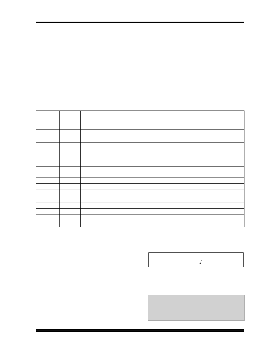
Figure 2-1 shows a typical 3-axis HCS473 RKE/PKE
application.
� The switch inputs have internal pull-down resis-
tors and integrated debouncing allowing a switch
to be directly connected to the inputs.
The transponder circuitry requires only the addition of
external LC-resonant circuits for inductive communica-
tion capability.
� The open-drain LED output allows an external
resistor for customization of LED brightness - and
current consumption.
� The DATA output can be directly connected to the
RF circuit or connected in conjunction with S3/
RFEN to a PLL.
2.1
Pinout Overview
A description of pinouts for the HCS473 can be found
in Table 2-1.
TABLE 2-1:
PINOUT SUMMARY
2.2
LF Antenna Considerations
A typical magnetic low frequency sensor (receiving
antenna) consists of a parallel inductor-capacitor circuit
that is sensitive to an externally applied magnetic sig-
nal. This LC circuit is tuned to resonate at the source
signal's base frequency. The real-time voltage across
the sensor represents the presence and strength of the
surrounding magnetic field. By amplitude modulating
the source's magnetic field, it is possible to transfer
data over short distances. This communication
approach is successfully used with distances up to 1.8
meters, depending on transmission strengths and sen-
sor sensitivity. Two key factors that greatly affect com-
munication range are:
1.
Sensor tuning
2.
A properly tuned sensor's relative sensitivity
An LC antenna's component values may be initially cal-
culated using the following equation. "Initially" because
there are many factors affecting component selection.
It is not this data sheet's purpose to present in-depth
details regarding LC antenna and their tuning. Please
refer to "Low Frequency Magnetic Transmitter Design
Application Note", AN232, for appropriate LF antenna
design details.
Pin Name
Pin
Number
Description
S0
1
Button input pin with Schmitt Trigger detector and internal pull-down resistor (Figure 2-3).
S1
2
Button input pin with Schmitt Trigger detector and internal pull-down resistor (Figure 2-3).
S2
3
Button input pin with Schmitt Trigger detector and internal pull-down resistor (Figure 2-3).
S3/RFEN
4
Multi-purpose input/output pin (Figure 2-4).
� Button input pin with Schmitt Trigger detector and internal pull-down resistor.
� RFEN output driver.
V
DDT
5
Transponder supply voltage. Regulated voltage output for strong inductive field.
LCX
6
Sensitive transponder input X (Figure 2-7). A strong signal on this pin is internally regulated
and supplied on V
DD
for low-battery operation/recharging.
LCY
7
Sensitive transponder input Y (Figure 2-7)
LCZ
8
Sensitive transponder input Z (Figure 2-7)
LCCOM
9
Transponder bias output (Figure 2-7)
V
SST
10
Transponder ground reference, must be connected to V
SS
.
V
SS
11
Ground reference
DATA
12
Transmission data output (Figure 2-5)
LED
13
Open drain LED output (Figure 2-6)
V
DD
14
Positive supply voltage
Note:
Microchip also has a confidential Applica-
tion Note on Magnetic Sensors (AN832C).
Contact Microchip for a Non-Disclosure
Agreement in order to obtain this applica-
tion note.
2F
1
LC
-----------
=
HCS473
DS40035C-page 6
Preliminary
2002 Microchip Technology Inc.
FIGURE 2-1:
HCS473 3-AXIS
APPLICATION
FIGURE 2-2:
HCS473 1-AXIS
APPLICATION
FIGURE 2-3:
S0/S1/S2 PIN DIAGRAM
FIGURE 2-4:
S3/RFEN PIN DIAGRAM
FIGURE 2-5:
DATA PIN DIAGRAM
RF
Circuit
HCS473
S0
S1
S2
V
DDT
LCX
LCY
V
DD
LED
DATA
V
SS
V
SST
LCCOM
LCZ
S3/RFEN
1
�F
100nF
V
DD
680pF
L
X
L
Y
L
Z
C
X
C
Y
C
Z
Note:
The 680pF capacitor prevents device instability - self
resonance.
RF
Circuit
HCS473
S0
S1
S2
V
DDT
LCX
LCY
V
DD
LED
DATA
V
SS
V
SST
LCCOM
LCZ
S3/RFEN
1
�F
100nF
V
DD
660 pF
100
L
X
C
X
100
Note:
Connect unused LC antenna inputs to LCCOM
through a 100
resistor for proper bias conditions.
R
PD
S0, S1, S2
Inputs
S3 Input/
RFEN
RFEN Output
V
DD
R
PD
NFET
PFET
Note:
R
PD
is disabled when driving RFEN.
V
DD
RDATA
DATA
NFET
PFET
DATA OUT
Note:
RDATA is disabled when the DATA line is driven.

2002 Microchip Technology Inc.
Preliminary
DS40035C-page 7
HCS473
FIGURE 2-6:
LED PIN DIAGRAM
FIGURE 2-7:
LCCOM/LCX/LCY/LCZ/
VSST PIN DIAGRAM
2.3
Architectural Overview
2.3.1
WAKE-UP LOGIC
The HCS473 automatically goes into a low-power
Standby mode once connected to a supply voltage.
Power is supplied to the minimum circuitry required to
detect a wake-up condition; button activation or LC sig-
nal detection.
The HCS473 will wake from Low-power mode when a
button input is pulled high or a signal is detected on a
LC low frequency antenna input pin. Waking involves
powering the main logic circuitry that controls device
operation. The button and transponder inputs are then
sampled to determine which input activated the device.
A button input activation places the device into Encoder
mode. A signal detected on the transponder input
places the device into Transponder mode. Encoder
mode has priority over Transponder mode such that
communication on the transponder input would be
ignored or perhaps interrupted if it occurred simulta-
neously to a button activation; ignored until the button
input is released.
2.3.2
ENCODER INTERFACE
Using the four button inputs, up to 15 unique control
codes may be transmitted.
LED
HV
Detect
Program
Weak
LED
V
DD
Mode
LCX/LCY/
LCZ Inputs
RECTIFIER and
REGULATOR
V
SST
10V
100
LC
Input
AMP
DET
and
DAMP
LCX
only
10V
100
BIAS
CURRENT
LCCOM
CLAMP
R
DAMP
Note:
S3 may not be used as a button input if the
RFEN option is enabled.

HCS473
DS40035C-page 8
Preliminary
2002 Microchip Technology Inc.
2.3.3
TRANSPONDER INTERFACE
The transponder interface on the HCS473 consists of
the following:
� The internal transponder circuitry has separate
power supply (V
DDT
) and ground (V
SST
) connec-
tions.
- The V
DDT
pin supplies power to the transpon-
der circuitry and also outputs a regulated volt-
age if the LCX antenna input is receiving a
strong signal; transponder is placed in a
strong LF field.
- The V
SST
pin supplies the ground reference
to the transponder circuitry and must be con-
nected to the V
SS
pin.
� LF input amplifier and envelope detector to detect
and shape the incoming low frequency excitation
signal.
� Three sensitive transponder inputs with over-volt-
age protection (LCX, LCY, LCZ).
� Incoming LF energy rectification and regulation on
the LCX input to supplement the supply voltage in
low-battery transponder instances.
� 10V zener input protection from excessive
antenna voltage resulting when proximate to very
strong magnetic fields.
� LCCOM pin used to bias the transponder reso-
nant circuits for best sensitivity.
� LF antenna clamping transistors for inductive
responses back to the transponder reader. The
antenna ends are shorted together, `clamped',
dissipating the oscillatory energy. The reader
detects this as a momentary load on its excitation
antenna.
� Damping transistors to increase LF communica-
tion reliability when using high Q-factor LC anten-
nae.
The LCCOM pin functions to bias the LCX, LCY, and
LCZ AGC amplifier inputs. The amplifier gain control
sets the optimum level of amplification in respect to the
incoming signal strength. The signal then passes
through an envelope detector before interpretation in
the logic circuit.
A block diagram of the transponder circuit is shown in
Figure 2-8.
FIGURE 2-8:
HCS473 TRANSPONDER
CIRCUIT
2.3.4
INTERNAL EEPROM
The HCS473 has an on-board non-volatile EEPROM
which is used to store:
� configuration options
- encryption keys
- serial number
- vehicle ID's
- baud rates
- ... see Section 3.1.4 and Section 3.2.1
� 64 bits of user memory
� synchronization counter.
All options are programmable during production, but
many of the security related options are programmable
only during production and are further read protected.
The user area allows storage of general purpose infor-
mation and is accessible only through the transponder
communication path.
During every EEPROM write, the device ensures that
the internal programming voltage is at an acceptable
level prior to performing the EEPROM write.
Rectifier/
Regulator
V
CCT
Noise
Filter
Signal In
Damp/Clamp
Control
LCX
LCY
LCZ
LCCOM

2002 Microchip Technology Inc.
Preliminary
DS40035C-page 9
HCS473
2.3.5
INTERNAL RC OSCILLATOR
The HCS473 runs on an internal RC oscillator. The
internal oscillator may vary �10% over the device's
rated voltage and temperature range for commercial
temperature devices. A certain percentage of indus-
trial temperature devices vary further on the slow side,
-20%, when used at higher voltages (V
DD
> 3.5V) and
cold temperature. The LF and RF communication
timing values are subject to these variations.
2.3.6
LOW VOLTAGE DETECTOR
The HCS473's battery voltage detector detects when
the supply voltage drops below a predetermined value.
The value is selected by the Low Voltage Trip Point
Select (VLOWSEL) configuration option (Section 3.3).
The low voltage detector result is included in encoder
transmissions (VLOW) allowing the receiver to indicate
when the transmitter battery is low (Section 3.1.4.6).
The HCS473 also indicates a low battery condition by
changing the LED operation (Section 3.1.5).
2.3.7
THE S3/RFEN PIN
The S3/RFEN pin may be used as a button input or RF
enable output to a compatible PLL. Select between S3
button input and RFEN functionality with the RFEN
configuration option (Table 2-2).
TABLE 2-2:
RFEN OPTION
RFEN
Resulting S3/RFEN Configuration
0
S3 button input pin with Schmitt Trigger
detector and internal pull-down resistor.
1
RFEN output driver.
S3 may not be used as a button input if the
RFEN option is enabled

HCS473
DS40035C-page 10
Preliminary
2002 Microchip Technology Inc.
NOTES:

2002 Microchip Technology Inc.
Preliminary
DS40035C-page 11
HCS473
3.0
DEVICE OPERATION
HCS473 operation depends on how the device is acti-
vated. The device exits Low-power mode either when a
switch input is pulled high or when a signal is detected
on an LC antenna input pin. Once activated, the device
determines the source of the activation and enters
Encoder mode or Transponder mode.
A button input activation places the device into Encoder
mode. A signal detected on the transponder input
places the device into Transponder mode. Encoder
mode has priority over Transponder mode such that
communication on the transponder input would be
ignored or perhaps interrupted if it occurred simulta-
neously to a button activation; ignored until the button
input is released.
3.1
Encoder mode
3.1.1
ENCODER ACTIVATION
3.1.1.1
Button Activation
The main way to enter Encoder mode is when the
wake-up circuit detects a button input activation; button
input transition from GND to V
DD
. The HCS473 control
logic wakes and delays a nominal switch debounce
time (T
DB
) prior to sampling the button inputs. The but-
ton input states, cumulatively called the button status,
determine whether the HCS473 transmits a code hop-
ping or seed transmission.
The transmission begins a time T
PU
after activation. It
consists of a stream of code words transmitted as long
as the switch input is held high or until a selectable
TSEL timeout occurs (see Section 3.1.4.16 for TSEL
options). A timeout returns the device to Low-power
mode, protecting the battery in case a button is stuck.
Additional button activations during a transmission will
immediately reset the HCS473, perhaps leaving the
current code word incomplete. The device will start a
new transmission which includes the updated button
status value.
Buttons removed during a transmission will have no
effect unless no buttons remain activated. If no button
activations remain, the minimum number of complete
code words will be completed (see Section 3.1.4.15 for
MTX options) and the device will return to Low Power
mode.
3.1.1.2
Proximity Activation
A second way to enter Encoder mode is if the proximity
activation option (PXMA) is enabled and the wake-up
circuit detects a wake-up sequence on an LC antenna
input pin. This form of activation is called Proximity
Activation as a code hopping transmission would be ini-
tiated when the device was proximate to a LF field.
3.1.2
TRANSMITTED CODE WORD
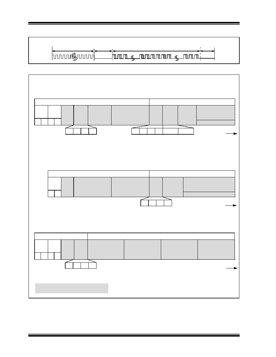
The HCS473 transmits a 69-bit code word in response
to a button activation or proximity activation, Figure 3-
1. The code word content varies with the two unique
transmission types; Hopping or Seed.
3.1.2.1
Hopping Code Word
Hopping code words are those transmitted during nor-
mal operation. Each Hopping code word contains a
preamble, header, 32 bits of encrypted data and up to
37 bits of fixed value data followed by a guard period
before another code word begins.
� The 32 bits of Encrypted Data include button sta-
tus bits, discrimination bits and the synchroniza-
tion counter value. The inclusion/omission of
overflow bits and size of both synchronization
counter and discrimination bit fields vary with the
CNTSEL option, Figure 3-2 and Section 3.1.4.5.
� The 37 bits of Fixed Code Data include queue
bits (if enabled), CRC bits, low voltage status and
serial number. The inclusion/omission of button
status and size of the serial number field vary with
the XSER option, Figure 3-2 and Section 3.1.4.3.
3.1.2.2
Seed Code Word
Seed code words are required when the system imple-
ments secure key generation. Seed transmissions are
activated when the button inputs match the value spec-
ified by the seed button code configuration option
(SDBT), Section 3.1.4.9.
Each Seed code word contains a preamble, header
and up to 69 bits of fixed data followed by a guard
period before another code word begins.
� The 69 bits of Fixed Code Data include queue
bits (if enabled), CRC bits, low voltage status, but-
ton status and the 60-bit seed value, Figure 3-2.
.
Note:
For additional information on K
EE
L
OQ
the-
ory and implementation, please refer to the
K
EE
L
OQ
introductory Technical Brief
(TB003).
HCS473
DS40035C-page 12
Preliminary
2002 Microchip Technology Inc.
FIGURE 3-1:
GENERAL CODE WORD FORMAT
FIGURE 3-2:
CODE WORD ORGANIZATION
Preamble
Header
Guard
Time
Data Bits
S2
S1
S0 S3
Synchronization
Counter
Synchronization
Counter
LSb
V
LOW
1-Bit
Fixed Code Portion (35 Bits)
CRC
2 Bits
V
LOW
1-Bit
SER 1
Most Sig 16 Bits
SER 0
Least Sig 16 Bits
BUT
4 Bits
DISCRIM
8 Bits
20 Bits
20
0
Hopping Code Portion Message (32 Bits)
C1 C0
MSb
67 Data bits
Transmitted LSb first.
Hopping Code:
Fixed Code Portion (37 Bits)
QUE
2 Bits
CRC
2 Bits
BUT
4 Bits
S2
S1
S0 S3
SER 0
Least Sig16 Bits
BUT
4 Bits
Counter
Overflow
2 Bits
DISCRIM
10 Bits
Synchronization
16 Bits
Counter
15
0
S2
S1
S0 S3
OVR1
OVR0
Hopping Code Portion Message (32 Bits)
Q1 Q0 C1 C0
MSb
LSb
69 Data bits
Transmitted LSb first.
SER 1
12 MSb's
Hopping Code:
CRC
2 Bits
V
LOW
1-Bit
BUT
4 Bits
SDVAL3
12 Most Sig Bits
1
1
1
1
SDVAL2
16 Bits
SDVAL1
16 Bits
SDVAL0
16 Least Sig Bits
C1 C0
LSb
MSb
Shaded 65 bits included in CRC calculation
69 Data bits
Transmitted LSb first.
Fixed Code Portion (9 Bits)
Seed Value (60 Bits)
Seed Code:
20-bit Synchronization Counter (CNTSEL=1)
16-bit Synchronization Counter (CNTSEL=0)
32-bit Serial Number (XSER = 1)
28-bit Serial Number (XSER = 0)
Button Queuing enabled (QUEN=1)
Button Queuing disabled (QUEN=0)
Queuing enabled (QUE = 1)
S2
S1
S0 S3
QUE
2 Bits
Q1 Q0
2002 Microchip Technology Inc.
Preliminary
DS40035C-page 13
HCS473
3.1.3
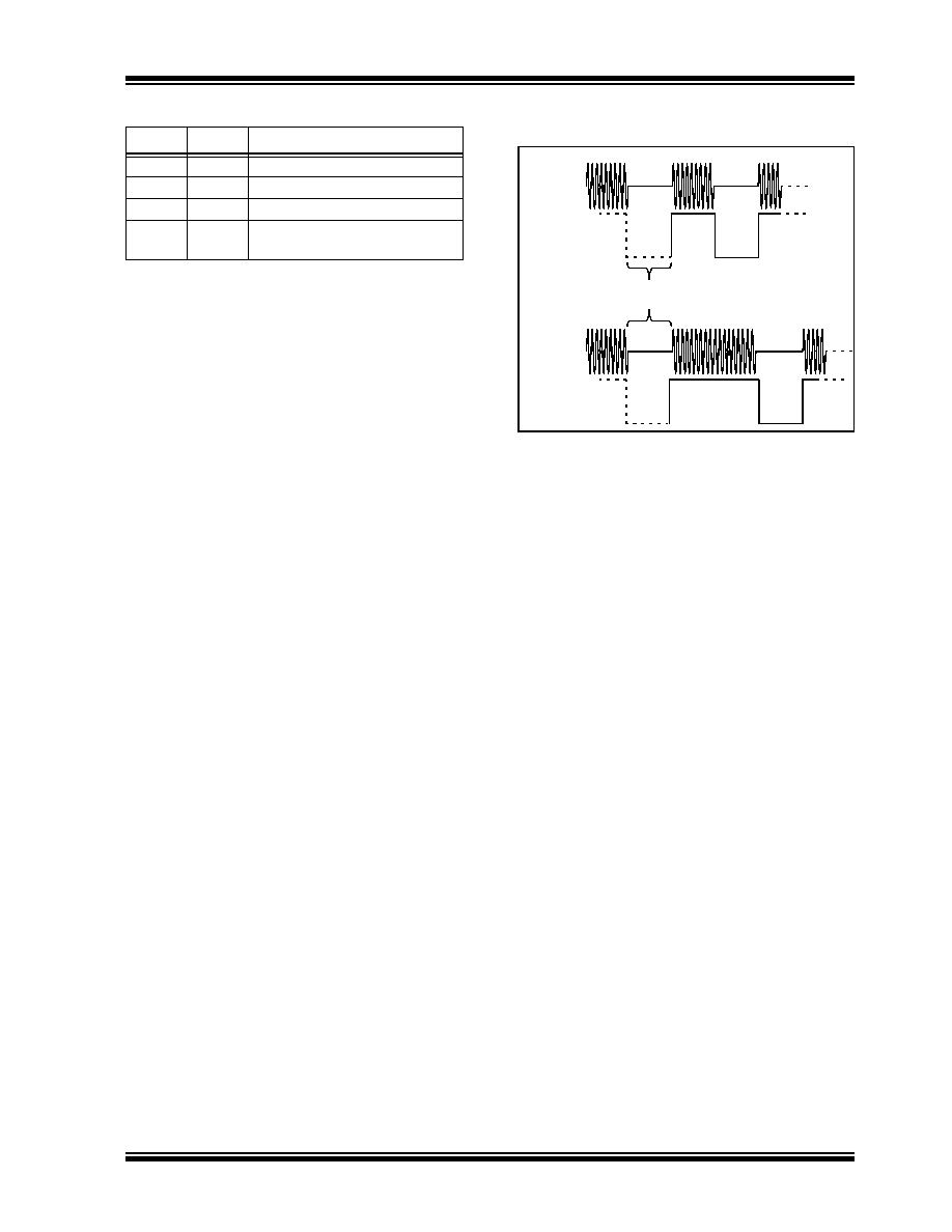
CODE HOPPING MODULATION
FORMAT
The data modulation format is selectable between
Pulse Width Modulation (PWM) and Manchester using
the modulation select (MSEL) configuration option.
Regardless of the modulation format, each code word
contains a leading preamble and a synchronization
header to wake the receiver and provide synchroniza-
tion events for the receive routine. Each code word also
contains a trailing guard time to separate code words.
Manchester encoding further includes a leading data `1'
START pulse and closing 1 RFT
E
STOP pulse around
each data block.
The same code word repeats as long as the same input
pins remain active, until a timeout occurs or a delayed
seed transmission is activated.
The modulated data timing is typically referred to in
multiples of a basic Timing Element (RFT
E
). `RF' T
E
because the DATA pin output is typically sent through a
RF transmitter to the decoder or transponder reader.
RFT
E
may be selected using the RF Transmission
Baud Rate (RFBSL) configuration option
(Section 3.1.4.13).
FIGURE 3-3:
PWM TRANSMISSION FORMAT (MSEL = 0)
FIGURE 3-4:
MANCHESTER TRANSMISSION FORMAT (MSEL = 1)
TOTAL TRANSMISSION
:
Preamble Sync Encrypt
Fixed
Guard
1 CODE WORD
Preamble Sync
Encrypt
LOGIC "1"
Guard
Time
Preamble
Encrypted
Portion
Fixed Code
Portion
LOGIC "0"
Header
T
E
T
E
T
E
CODE WORD
TOTAL TRANSMISSION:
CODE WORD
Guard
Header
Encrypted
Fixed Code
START bit
STOP bit
Time
Portion
Portion
bit 0 bit 1 bit 2
LOGIC "0"
LOGIC "1"
T
E
T
E
Preamble
Preamble Sync Encrypt
Fixed
Guard
1 CODE WORD
Preamble Sync
Encrypt

HCS473
DS40035C-page 14
Preliminary
2002 Microchip Technology Inc.
3.1.4
ENCODER MODE OPTIONS
The following HCS473 configuration options configure
transmission characteristics of the information exiting
the DATA pin:
� Modulation select (MSEL)
� Header select (HSEL)
� Extended serial number (XSER)
� Queue counter enable (QUEN)
� Counter select (CNTSEL)
� Low voltage trip point (VLOWSEL)
� PLL interface select (AFSK)
� RF enable output (RFEN)
� Seed button code (SDBT)
� Time before Seed (SDTM)
� Limited Seed (SDLM)
� Seed mode (SDMD)
� RF baud rate select (RFBSL)
� Guard time select (GSEL)
� Minimum code words (MTX)
� Timeout select (TSEL)
� Long preamble enable (LPRE)
� Long preamble length (LPRL)
� Preamble duty cycle (PRD)
The following sections detail each configuration's avail-
able options. All timing values specified are subject to
the specified oscillator variation.
3.1.4.1
Modulation Format (MSEL)
The Modulation format option selects the modulation
format for data output from the DATA pin; most often
transmitted via RF.
MSEL options:
� Pulse Width Modulation (PWM), Figure 3-3
� Manchester Modulation, Figure 3-4
3.1.4.2
Header Select (HSEL)
The synchronization header is typically used by the
receiver to adjust bit sampling appropriate to the trans-
mitter's current speed; as the transmitter's RC oscilla-
tor varies with temperature and voltage, so will the
transmission's timing.
HSEL options:
� 4 RF
TE
� 10 RF
TE
3.1.4.3
Extended Serial Number (XSER)
The Extended Serial Number option determines
whether the HCS473 transmits a 28 or 32-bit serial
number.
When configured for a 28-bit serial number, the Most
Significant nibble of the 32 bits reserved for the serial
number is replaced with a copy of the 4-bit button sta-
tus, Figure 3-2.
XSER options:
� 28-bit serial number
� 32-bit serial number
3.1.4.4
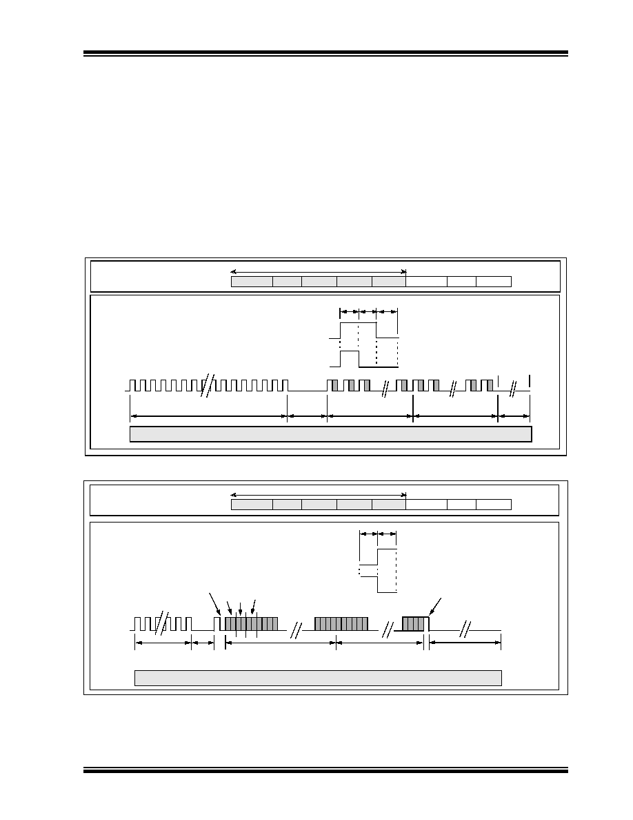
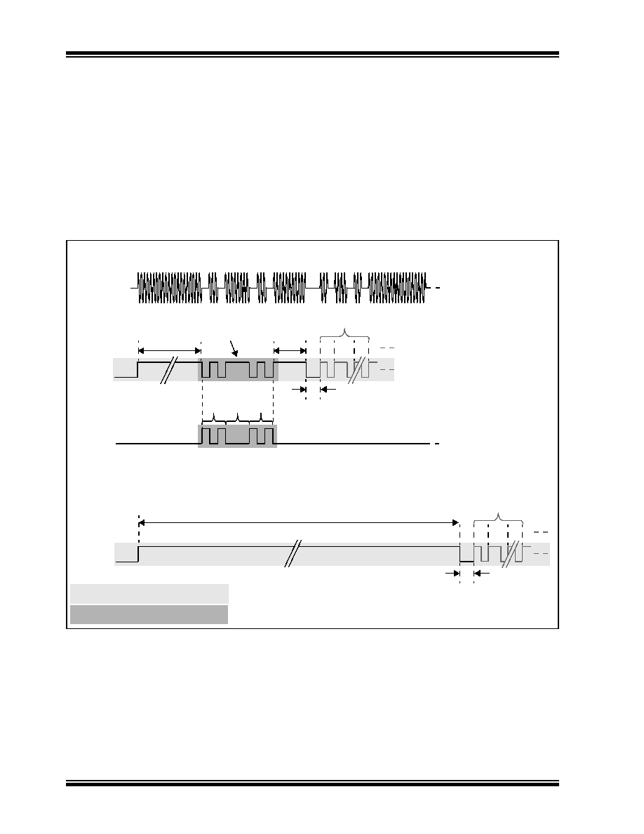
Queue Counter (QUEN)
The QUE counter can be used to request secondary
decoder functions using only a single transmitter but-
ton. Typically a decoder must keep track of incoming
transmissions to determine when a double button press
occurs, perhaps an unlock all doors request. The QUE
counter removes this burden from the decoder by
counting multiple button presses and including the
QUE counter value in the last two bits of the 69-bit code
word, (Figure 3-2). If QUEN is disabled, the transmis-
sion will consist only of 67 bits as the QUE bits field is
not transmitted.
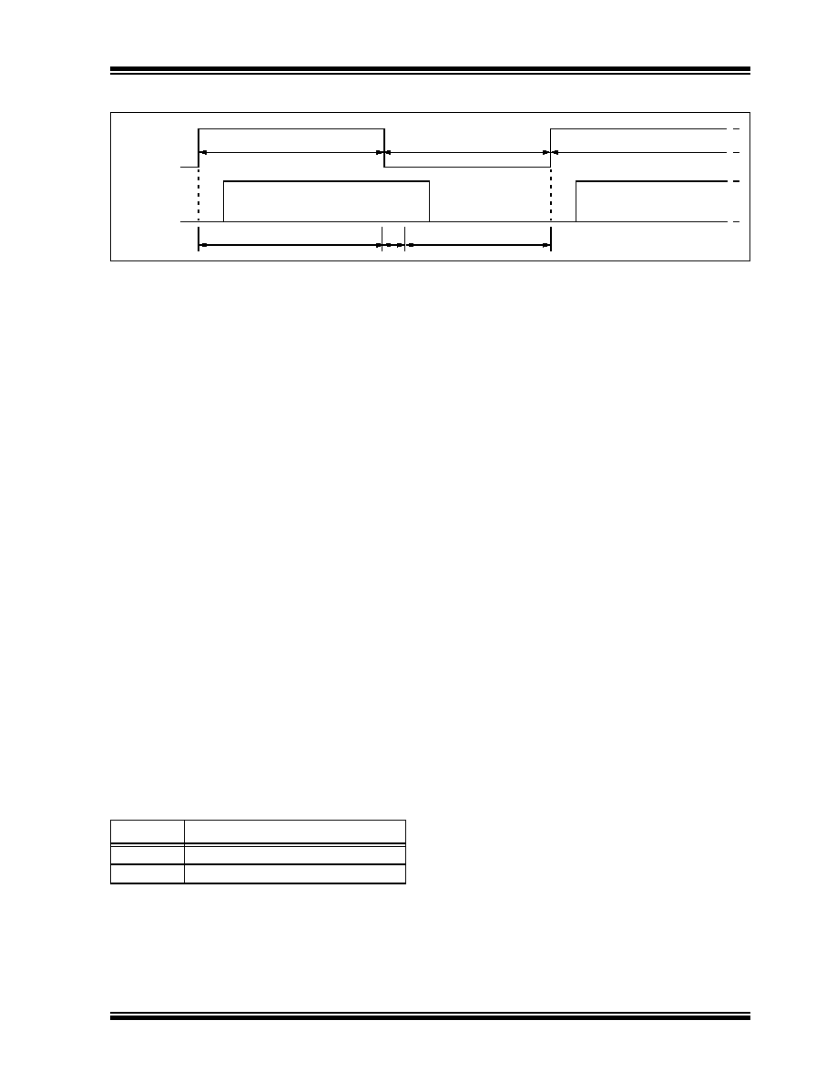
Que counter functionality is enabled with the QUEN
configuration option. The 2-bit QUE counter is incre-
mented each time an active button input is released for
at least the Debounce Time (T
DB
), then re-activated
(button pressed again) within the Queue Time (T
QUE
),
Figure 3-5. The counter increments up from 0 to a max-
imum of 3, returning to 0 only after a different button
activation or after button activations spaced greater
than the Queue Time (T
QUE
) apart.
The current transmission aborts, after completing the
minimum number of code words (Section 3.1.4.15),
when the active button inputs are released. A button re-
activation within the queue time (T
QUE
) then initiates a
new transmission (new synchronization counter,
encrypted data) using the updated QUE value. Button
combinations are queued the same as individual but-
tons.
2002 Microchip Technology Inc.
Preliminary
DS40035C-page 15
HCS473
FIGURE 3-5:
QUE COUNTER TIMING DIAGRAM
3.1.4.5
Counter Select (CNTSEL)
The counter select option selects between a 16-bit or
20-bit counter. This option changes the way the 32-bit
hopping portion is constructed, as indicated in
Figure 3-2. The 16-bit counter format additionally
includes two overflow bits for increasing the synchroni-
zation counter range, see Section 3.1.7.
CNTSEL options:
� 16-bit synchronization counter
� 20-bit synchronization counter
3.1.4.6
Low Voltage Trip Point Select
(VLOWSEL)
The HCS473's battery voltage detector detects when
the supply voltage drops below a predetermined value.
The value is selected by the Low Voltage Trip Point
Select (VLOWSEL) configuration option (Table 3-6).
VLOWSEL options:
� 2.2V trip point
� 3.3V trip point
The low voltage detector result (VLOW) is included in
Hopping code transmissions allowing the receiver to
indicate when the transmitter battery is low (Figure 3-
2). The HCS473 also indicates a low battery condition
by changing the LED operation (Section 3.1.5).
The HCS473 samples the internal low voltage detector
at the end of each code word's first preamble bit. The
transmitted VLOW status will be a `0' as long as the low
voltage detector indicates V
DD
is above the selected
low voltage trip point. VLOW will change to a `1' if V
DD
drops below the selected low voltage trip point.
TABLE 3-1:
VLOW STATUS BIT
3.1.4.7
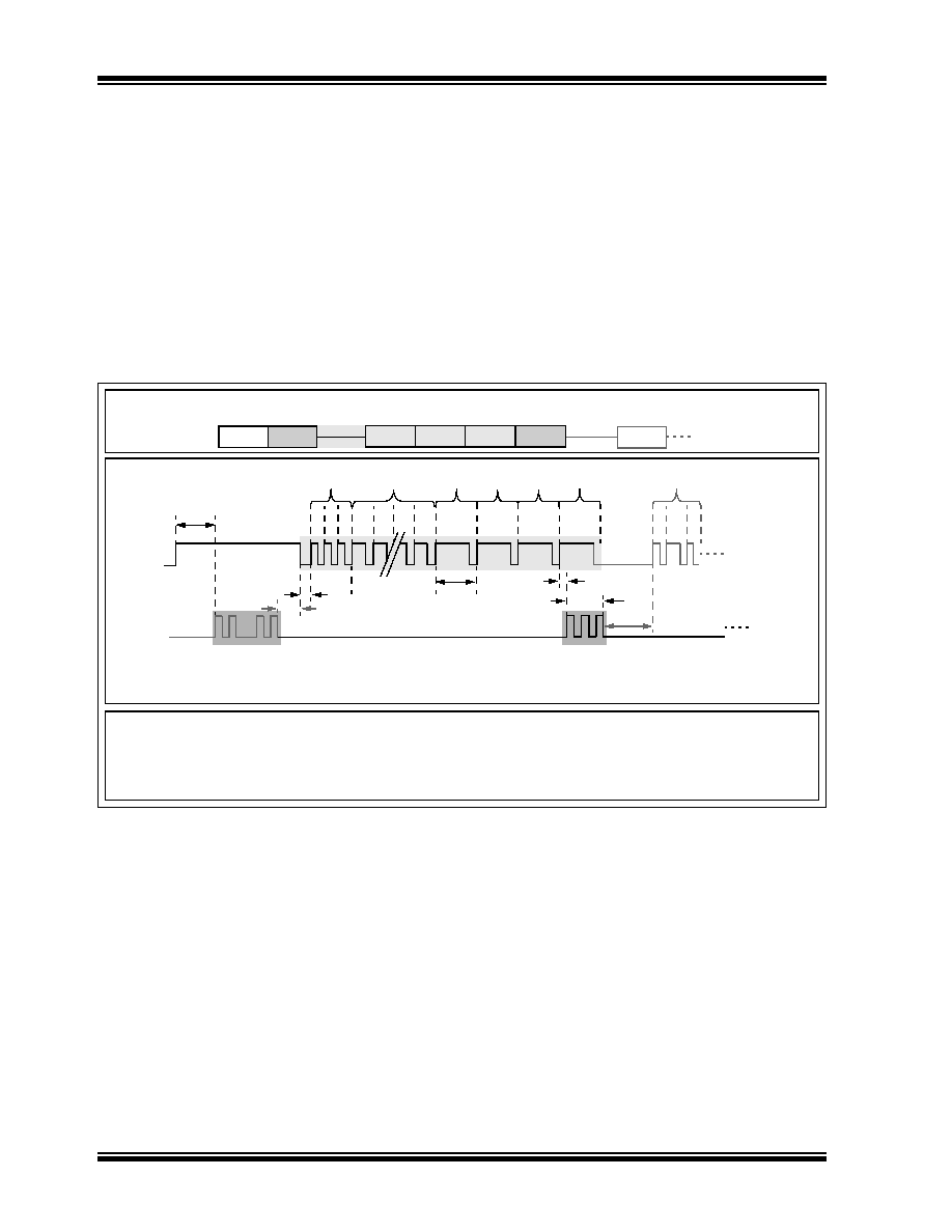
PLL Interface Select (PLLSEL)
The S3/RFEN pin may be configured as an RF enable
output to an RF PLL. The pin's behavior is coordinated
with the DATA pin to activate a typical PLL in either
ASK or FSK mode.
The PLL Interface (PLLSEL) configuration option con-
trols the output as shown for Encoder operation in
Figure 3-6. Please refer to Section 3.2.8 for RFEN
behavior during LF communication.
PLLSEL options:
� ASK PLL Setup
� FSK PLL Setup
3.1.4.8
RF Enable Output (RFEN)
The S3/RFEN pin of the HCS473 can be configured to
function as an RF enable output signal. When enabled,
the pin is driven high whenever data is transmitted
through the DATA pin; the S3/RFEN pin can therefore
not be used as an input in this configuration. The RF
enable option bit functions in conjunction with the PLL
interface select option, PLLSEL.
RFEN options:
� S3/RFEN pin functions as S3 switch input only
� S3/RFEN pin functions as RFEN output only
t
T
DB
Button Input
Sx
Code Words
Transmitted
T
DB
t T
QUE
QUE1:0 = 00
2
Synch CNT = X
Transmission:
QUE1:0 = 01
2
Synch CNT = X+1
Transmission:
T
DB
1st Button Press
All Buttons Released
2nd Button Press
VLOW
Description
0
V
DD
is above selected trip voltage
1
V
DD
is below selected trip voltage
HCS473
DS40035C-page 16
Preliminary
2002 Microchip Technology Inc.
FIGURE 3-6:
ENCODER OPERATION: RF ENABLE/ASK/FSK OPTIONS
3.1.4.9
SEED Button Code (SDBT)
SDBT selects which switch input(s) activate a seed
transmission. Seed transmissions are disabled by
clearing all 4 bits. If a button combination is pressed
that matches the 4-bit SDBT value, a seed code word
is transmitted as configured by the SDTM, SDLM and
SDMD options (see following sections).
The binary bit order is S3-S2-S1-S0. For example, if
you want the combination of S2 and S0 to activate a
seed transmission, use SDBT=0101
2.
SDBT options:
� Seed is transmitted when SDBT flags match the
button input flags
� SDBT = 0000
2
disables seed capability.
3.1.4.10
Time Before Seed (SDTM)
The time before seed option selects the delay from
device activation until the seed code words are trans-
mitted. If the delay is not zero, the HCS473 transmits
hopping code words until the selected time, then trans-
mits seed code words.
As code words are always completed, the seed code
word begins the first code word after the specified time.
SDTM options:
� 0s - seed code words begin immediately
� 0.8s
� 1.6s
� 3.2s
3.1.4.11
Limited Seed (SDLM)
The limited seed option may be used to disable seed
transmission capability after a configurable number of
transmitter activations; limiting a transmitter's ability to
be learned into a receiver. Specifically, seed transmis-
sions are disabled when the synchronization counter's
LSB increments from 7Fh to 80h.
SDLM options:
� unlimited seed capability
� limited seed capability - counter value dependent
3.1.4.12
SEED Mode (SDMD)
The Seed mode option selects between User and Pro-
duction seed modes. Production mode functions as a
special time before seed case (SDTM).
With Production mode enabled, a seed button code
activation triggers MTX hopping code words followed
by MTX seed code words. Production mode functional-
ity is disabled when the synchronization counter's LSB
increments from 7Fh to 80h.
SDMD options:
� User
� Production
3.1.4.13
RF Baud Rate Select (RFBSL)
The timing of code word data modulated on the DATA
pin is referred to in multiples of a basic Timing Element
RFT
E
. `RF' T
E
because the DATA pin output is typically
sent through a RF transmitter to the decoder or tran-
sponder reader.
RFT
E
may be selected using the RF Baud Rate Select
(RFBSL) configuration option. RF
TE
accuracy is sub-
ject to the oscillator variation over temperature and
voltage.
RFBSL options:
� 100
�s RFT
E
� 200
�s RFT
E
� 400
�s RFT
E
� 800
�s RFT
E
SWITCH
S3/RFEN
DATA
S3/RFEN
DATA
T
PLL
ASK:
T
PU
Code Word
Code Word
Code Word
Code Word
Code Word
Code Word
Code Word
Code Word
FSK:
Note:
Configuring S3/RFEN as RFEN (see
Section 3.1.4.8) prevents the use of S3 to
trigger a seed transmission.
2002 Microchip Technology Inc.
Preliminary
DS40035C-page 17
HCS473
3.1.4.14
Guard Time Select (GSEL)
The guard time (T
G
) select option determines the time
between consecutive code words when no data is
transmitted. The guard time may be selected in conjuc-
tion with the RF baud rate and preamble duty cycle to
control time-averaged power output for transmitter cer-
tification.
GSEL options:
� 3 RF
TE
� 6.4 ms
� 51.2 ms
� 102.4 ms
3.1.4.15
Minimum Code Words (MTX)
The Minimum Code Words (MTX) configuration option
determines the minimum number of code words trans-
mitted when a momentary switch input is taken high for
more than T
PU
, or when a proximity activation occurs.
MTX options:
� 1 code word
� 2 code words
� 4 code words
� 8 code words
3.1.4.16
Timeout Select (TSEL)
The HCS473's Timeout function prevents battery drain
should a switch input remain high (stuck button) longer
than the selectable TSEL time. After the TSEL time, the
device will return to Low-power mode.
The device will stop transmitting in Low-power mode
but there will be leakage across the stuck button input's
internal pull-down resistor. The current draw will there-
fore be higher than if no button were stuck.
TSEL options:
� 4s
� 8s
� 16s
� 32s
3.1.4.17
Long Preamble Enable (LPRE)
Enabling the Long Preamble configuration option
extends the first code word's preamble to a `long' pre-
amble time LPRL
;
allowing the receiver more time to
wake and bias before the data bits arrive. The longer
preamble will be a square wave at the selected RFT
E
.
Subsequent code words begin with the standard pre-
amble length.
LPRE options:
� Standard 16 high pulse preamble
� Long preamble, duration defined by LPRL
3.1.4.18
Long Preamble Length (LPRL)
The long preamble length option selects the first code
word's preamble length when the long preamble option
(LPRE) is enabled. Only the first code word begins with
the long preamble, subsequent code words begin with
the standard 16 high pulses preamble.
LPRL options:
� 75 ms
� 100 ms
3.1.4.19
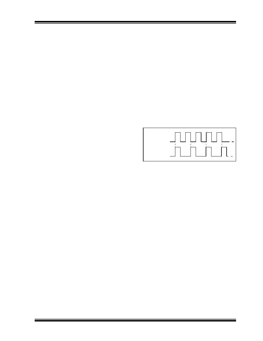
Preamble Duty Cycle (PRD)
The preamble duty cycle can be set to either 33% or
50% to limit the average power transmitted, Figure 3-7.
PRD options:
� 50% Duty Cycle
� 33% Duty Cycle
FIGURE 3-7:
PREAMBLE FORMATS
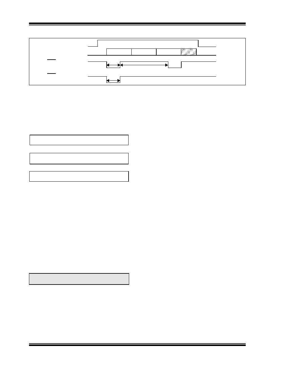
3.1.5
LED OPERATION
The LED pin output varies depending on whether the
device V
DD
is greater than V
LOWSEL
(a good battery) or
below V
LOWSEL
(a flat battery).
The LED pin will periodically be driven low as long as
the device is transmitting and the battery is good. If the
supply voltage drops below the specified V
LOWSEL
trip
point, the LED pin will be driven low only once for any
given device activation so long as the low battery con-
dition remains (Figure 3-8). If the battery voltage recov-
ers during the transmission, the LED will begin blinking
again.
T
E
T
E
T
E
2T
E
33% Duty Cycle
50% Duty Cycle
HCS473
DS40035C-page 18
Preliminary
2002 Microchip Technology Inc.
FIGURE 3-8:
LED OPERATION
3.1.6
CYCLE REDUNDANCY CHECK
(CRC)
The decoder can use the CRC bits to check the data
integrity before processing begins. The CRC is calcu-
lated on the previously transmitted bits (Figure 3-2),
detecting all single bit and 66% of all double bit errors.
EQUATION 3-1:
CRC CALCULATION
and
with
and Di
n
the nth transmission bit 0
n 64
3.1.7
COUNTER OVERFLOW BITS
(OVR1, OVR0)
The Counter Overflow Bits may be utilized to increase
the 16-bit synchronization counter range from the nom-
inal 65,535 to 131,070 or 196,605. The bits do not exist
when the device is configured for 20-bit counter opera-
tion.
The bits must be programmed during production as `1's
to be utilized. OVR0 is cleared the first time the syn-
chronization counter wraps from FFFFh to 0000h.
OVR1 is cleared the second time the synchronization
counter wraps to zero. The two bits remain at `0' after
all subsequent counter wraps.
3.1.8
DISCRIMINATION VALUE (DISC)
The Discrimination Value is typically used by the
decoder in a post-decryption check. It may be any
value, but in a typical system it will be programmed
equal to the Least Significant bits of the serial number.
The discrimination bits are part of the information that
form the encrypted portion of the transmission
(Figure 3-2). After the receiver has decrypted a trans-
mission, the discrimination bits are checked against the
receiver's stored value to verify that the decryption pro-
cess was valid; appropriate decryption key was used. If
the discrimination value was programmed as the LSb's
of the serial number then it may merely be compared to
the respective bits of the received serial number.
The discrimination bit field size varies with the counter
select (CNTSEL) option (Figure 3-2).
3.2
Transponder Mode
The HCS473's Transponder mode allows it to function
as a bi-directional communication transponder. Com-
mands are received on the LC pins, responses may be
returned on either the LC pins or DATA pin for short
range LF or long range RF responses, respectively.
Transponder mode capabilities include:
� A bi-directional challenge and response sequence
for IFF validation.
� Read selected EEPROM areas.
� Write selected EEPROM areas.
� Request a code hopping transmission.
� Proximity Activation of a code hopping transmis-
sion.
� Address an individual transponder when multiple
units are within the LF field; device selection for
anticollision communication purposes.
SWITCH Sx
LED -
DATA
T
LEDON
T
LEDOFF
Code Word
Code Word
Code Word
T
LEDON
V
DD
>V
LOWSEL
(good battery)
LED - V
DD
V
LOWSEL
(flat battery)
Note:
See Section 4.0, Programming Specs, for
information on programming OVR bits.
CRC 1
[ ]
n 1
+
CRC 0
[ ]
n
Di
n
=
CRC 0
[ ]
n 1
+
CRC 0
[ ]
n
Di
n
(
) CRC 1
[ ]
n
=
CRC 1 0
,
[
]
0
0
=

2002 Microchip Technology Inc.
Preliminary
DS40035C-page 19
HCS473
3.2.1
TRANSPONDER OPTIONS
The following HCS473 configuration options influence
the device behavior when in Transponder mode:
� Preamble length select (TPRLS)
� LF Demodulator (LFDEMOD)
� LF Baud rate select (LFBSL)
� Anticollision (ACOL)
� Proximity Activation (PXMA)
� Intelligent Damping (DAMP)
� LC response Enable (LCRSP)
� RF response Enable (RFRSP)
� Skip Field Acknowledge (SKIPACK)
The following sections describe these options in detail.
3.2.1.1
Transponder Preamble Length
Select (TPRLS)
Data responses through the DATA pin use the format
determined by the Encoder mode options, with one
exception/option to shorten the response time. The
response's preamble can be reduced to 4 high pulses
by setting the transponder preamble length select
option. This only affects the responses as a result of
transponder communication (proximity activation trans-
missions included), not responses resulting from but-
ton input activations. The 4 high pulse short preamble
will be at the same duty cycle defined by the preamble
duty cycle Encoder mode option (PRD).
TABLE 3-2:
TRANSPONDER PREAMBLE
LENGTH SELECT (TPRLS)
3.2.1.2
LF Demodulator (LFDEMOD)
The HCS473 has a LF Demodulator mode useful for
debugging antenna hardware.
Enabling LFDEMOD limits the device to demodulator
only mode. After receiving an appropriate wake-up
sequence, the device enters a loop demodulating the
signal on the LC pins and outputting the resulting digital
representation on the LED pin. The HCS473 remains in
this mode until no edges are detected on the LC pins
for T
DEMOD
, upon which it will return to Low-power
mode; requiring another wake-up sequence to further
demodulate data.
The demodulated signal on the LED pin is accurate to
within +/-10
�s of the signal on the LC pins. The injected
signal will have baud rate limitations based on the
HCS473's internal filter charge and discharge times,
Section 3.2.6.
The filter times discussed in Section 3.2.6 will be easily
seen in Demodulator mode. The internal filter delay
may be isolated by communicating to the HCS473
inputting the digital signal into LCX and observing the
signal plus internal filter delays on the LED pin.
LFDEMOD options:
� Disabled - device functions normally
� Enabled - device demodulates signal on LC pins,
outputting digital result on the LED pin.
3.2.1.3
LF Baud Rate Select (LFBSL)
The LF Baud rate select option allows the user to adjust
the basic pulse width element (LF
TE
) used for tran-
sponder communication.
LFBSL options:
� 100
�s LF
TE
� 200
�s LF
TE
� 400
�s LF
TE
� 800
�s LF
TE
All communication to and from the HCS473 through the
LC transponder pins will use the selected LF
TE
. RF
acknowledges to LF communication, through the DATA
pin, will also use the selected LF
TE
.
3.2.1.4
Anticollision (ACOL)
Multiple transponders in the same inductive field will
simultaneously respond to inductive commands.
Enabling anticollision prevents multiple HCS473
responses from 'colliding'. Hence the term `anticolli-
sion.'
When anticollision (ACOL) is enabled, the first com-
mand received after the device wakes must be either
the SELECT TRANSPONDER or ANTICOLLISION
OFFcommand before the HCS473 will respond to any
other command.
The ANTICOLLISION OFF command may be used to
temporarily bypass anticollision requirements for a sin-
gle communication sequence. It allows communication
with an anticollision enabled HCS473 if the VID and
TID are not known (perhaps during a learning
sequence). See Section 3.2.3.7 for further anticollision
off details.
The SELECT TRANSPONDER command allows the
addressing of and communication to an individual
HCS473, regardless if multiple devices are in the field
(Section 3.2.3.1).
Note:
The long preamble enable Encoder mode
option (LPRE) holds priority over the tran-
sponder preamble length option.
TPLS
LPRE
Description
0
0
Normal - 16 high pulses
X
1
Long - LPRL determines length
1
0
Short - 4 high pulses
Note:
Damping is disabled when in Demodulator
mode.

HCS473
DS40035C-page 20
Preliminary
2002 Microchip Technology Inc.
The HCS473 anticollision method is that all devices
trained to a given vehicle will have the same 12-bit
vehicle identifier (VID); Most Significant 12 bits of the
device identifier, Table 3-3. The device identifier of up
to 16 transponders trained to access a given vehicle
will differ only in the 4 LSb's. These 4 bits are referred
to as the token identifier (TID).
TABLE 3-3:
DEVICE ID
The vehicle ID associates the HCS473 with a given
vehicle and the token ID makes it a uniquely address-
able (selectable) 1 of 16 possible devices authorized to
access the vehicle.
Two unique device identifiers are available allowing the
HCS473 to be used with two different vehicles. The
HCS473 responds if the presented VID and TID match
either of the two programmed identifiers.
SELECT TRANSPONDER may still be performed on
devices not configured to require anticollision; commu-
nication can still be isolated to one of multiple devices
in the field. Equally, the same devices will respond to all
command sequences not preceded by the SELECT
TRANSPONDER sequence.
3.2.1.5
Proximity Activation (PXMA)
Enabling the Proximity Activation configuration option
allows the HCS473 to transmit a hopping code trans-
mission in response to detecting an appropriate wake-
up pulse on an LC input pin.
The HCS473 sends a wake-up sequence Acknowl-
edge in response to detecting the LF field (Figure 3-
11). The device then waits T
CMD
for the LF field's falling
edge followed by the normal T
CMD
window waiting for a
transponder command to begin. If no command is
received, a code hopping transmission is generated
and the minimum code words (set with MTX option) are
transmitted. When the transmission completes, the
HCS473 waits a T
CMD
window for a new command to
begin. If no command is received the device returns to
SLEEP.
Proximity activations are not repeatedly activated when
the device is in the presence of a continuous LF field
(computer monitor, tv,...). The HCS473 must receive an
appropriate wake-up sequence to activate each trans-
mission.
The button status used in the proximity activated code
hopping transmission clears the S0, S1, S2 and S3 but-
ton status flags.
3.2.1.6
Intelligent Damping (DAMP)
A high Q-factor LC antenna circuit connected to the
HCS473 will continue to resonate after a strong LF field
is removed, slowly decaying. The slow decay makes
fast communication near the reader difficult as the
resulting extended high time makes the following low
time disappear.
The Intelligent damping option enables a pulsed, resis-
tive short from the LC pins to LCCOM when the
HCS473 is expecting the incoming LC signal level to go
low. These pulses damp the antenna, dissipating reso-
nant energy for a quicker decay time when the field is
switched off.
The damping pulses are applied between the LCCOM
pin and the individual LC pins, starting 1.2 LF
TE
from
detecting the bit's rising edge and repeating until the
LC input goes low. Damp pulse width is 6
�s, beginning
every 44
�s as shown in Figure 3-9.
FIGURE 3-9:
INTELLIGENT DAMPING
3.2.1.7
Response Options (RFRSP,
LCRSP)
HCS473 responses may optionally be returned on the
DATA pin for long-range RF responses and/or LC pins
for short-range LF responses (Table 3-4). Responses
include both Acknowledge sequences and data
responses.
The options controlling the response path are:
� LC response option (LCRSP)
� RF response option (RFRSP)
If both RF and LF responses are enabled, Acknowl-
edge pulses will occur simultaneously on the DATA and
LC pins; using the LF
TE
baud rate (Figure 3-11,
Figure 3-19). Data responses will not occur simulta-
neously. The RF response on the DATA pin will occur
first (following the designated Encoder mode format),
immediately followed by the LF response on the LC
pins (Figure 3-20).
16-bit Device ID (DEVID)
15
14
13
12
11
10
9
8
7
6
5
4
3
2
1
0
VID
TID
11 10 9
8
7
6 5 4 3 2 1 0 3 2 1 0
Note:
Damping will not reduce the HCS473 inter-
nal LF analog filter discharge time, T
FILTF
(Section 3.2.6).
T
DAMP
LC Output
Level
Field on
LC pins
No Damping
With Damping
Damping Pulses
Signal
2002 Microchip Technology Inc.
Preliminary
DS40035C-page 21
HCS473
TABLE 3-4:
HCS473 RESPONSE OPTIONS
3.2.1.8
Skip Field Acknowledge (SKIPACK)
The initial Field Acknowledge sequence, occurring dur-
ing the wake-up pulse, may be disabled by enabling the
Skip Field Acknowledge configuration option (SKI-
PACK=1). Omitting the ACK slightly minimizes a
HCS473's average communication current draw, but
conversely will increase average authentication time as
the wake-up pulse must then be the maximum start-up
filter charge time, T
SF
MAX
.
3.2.2
TRANSPONDER COMMUNICATION
Data to and from the HCS473 is always sent Least Sig-
nificant bit first. The data length and modulation format
vary with the particular command sequence and the
transmission path.
3.2.2.1
LC Communication Format
Commands from the transponder reader to the
HCS473 as well as the responses from the HCS473
over the low frequency path (LC pins) are Pulse Posi-
tion Modulated (PPM) according to Figure 3-10.
Communication from the transponder reader to a
HCS473 is via the reader amplitude shifting a 125kHz
low frequency (LF) field.
LF responses back to the transponder reader are
achieved by the HCS473 applying a low-resistance
short from the LC pins to LCCOM (configuration option
LCRSP enables LF talkback). This short across the
antenna inputs is detected by the reader as a load on
its 125kHz transmitting antenna.
See Section 5.4 for further details on inductive commu-
nication principles.
FIGURE 3-10:
LC PIN PULSE POSITION
MODULATION (PPM)
3.2.2.2
RF DATA Communication Format
The RF responses on the DATA pin vary with the infor-
mation being returned.
� Acknowledge responses are based on the LF
TE
.
� Data code words responses are based on the
RF
TE
, using the format determined by the
Encoder mode options, Section 3.1.4.
3.2.2.3
Wake-up Sequence
The transponder reader initiates each communication
sequence by turning on the low frequency field, then
waits for a HCS473 to Acknowledge the field.
The HCS473 enters Transponder Mode after detecting
a signal on any LC low frequency antenna input pin that
has remained high for at least the start-up filter time
T
SF
, Table 7-5. The device then responds with a Field
Acknowledge sequence indicating that it has detected
the LF field, is in Transponder Mode and is ready to
receive commands (Figure 3-11). The wake-up pulse's
falling edge must then occur within T
CMD
of the end of
the Field Acknowledge sequence.
The Field Acknowledge sequence may optionally be
disabled by enabling the Skip Field ACK configuration
option, Section 3.2.1.8.
In both cases, the first command bit must begin within
T
CMD
of the wake-up pulse's falling edge or the
HCS473 will return to Low Power mode.
RFRSP
LCRSP
Description
0
0
No response
0
1
Response over the LC pins
1
0
Response through the DATA pin
1
1
Response through the DATA pin
first and then the LC pins
START or
previous bit
1LF
TE
2LF
TE
`0'
`1'
1LF
TE
1LF
TE
Digital
Representation
125kHz
Digital
Representation
125kHz
HCS473
DS40035C-page 22
Preliminary
2002 Microchip Technology Inc.
3.2.2.4
Command Sequence
The transponder reader follows the HCS473's Field
Acknowledge by sending the desired 3-bit command,
3-bit option or address, associated data and CRC;
each as required. LF commands are Pulse Position
Modulated (PPM) as shown in Figure 3-10. The last bit
(CRC bit) should be followed by leaving the field on for
T
FINH
.
T
FINH
should be appropriately adjusted to receive con-
secutive commands or LF responses. See
Section 3.2.4 and Section 3.2.5 for LF response and
consecutive command considerations.
FIGURE 3-11:
HCS473 TRANSPONDER WAKE-UP SEQUENCE
Communication from reader to HCS473
Communication from HCS473 to reader
SKIPACK = 1 - Field Acknowledge is not sent
Inductive
(LC)
T
SF
Command
T
CMD
T
SF
MAX
SKIPACK = 0 - Field Acknowledge sent when device wakes
Inductive
(LC)
RF
Response
(DATA)
125kHz Field
(on LC pins)
T
CMD
bit0
bit1
bit2
Command
bit
0
bit
1
bit
2
T
CMD
3LF
TE
3LF
TE
3LF
TE
3LF
TE
Simultaneous LF
Acknowledge
(LFRSP=1)
RF Acknowledge
(RFRSP=1)

2002 Microchip Technology Inc.
Preliminary
DS40035C-page 23
HCS473
3.2.3
TRANSPONDER COMMANDS
TABLE 3-5:
LIST OF AVAILABLE TRANSPONDER COMMANDS
Command
Option
Description
Select Transponder
(Section 3.2.3.1)
000
2
-
Select HCS473, used to isolate communication to a single HCS473
Present Transport Code
(1)
(Section 3.2.3.2)
001
2
-
Used to gain write access to the device EEPROM memory locations
Identify Friend or Foe (IFF)
(1)
(Section 3.2.3.3)
010
2
000
2
32-bit IFF using the Transponder Key
001
2
16-bit IFF using the Transponder Key
010
2
32-bit IFF using the Encoder Key
011
2
16-bit IFF using the Encoder Key
Read EEPROM
(1)
(Section 3.2.3.4)
100
2
000
2
Read 16-bit User EEPROM 0
001
2
Read 16-bit User EEPROM 1
010
2
Read 16-bit User EEPROM 2
011
2
Read 16-bit User EEPROM 3
100
2
Read Most Significant 16 bits of the Serial Number
101
2
Read Least Significant 16 bits of the Serial Number
110
2
Read 16-bit Device Identifier #1 (12-bit Vehicle ID #1 and 4-bit Token ID #1)
111
2
Read 16-bit Device Identifier #2 (12-bit Vehicle ID #2 and 4-bit Token ID #1)
Write EEPROM
(1) (2)
(Section 3.2.3.5)
101
2
000
2
Write 16-bit User EEPROM 0
001
2
Write 16-bit User EEPROM 1
010
2
Write 16-bit User EEPROM 2
011
2
Write 16-bit User EEPROM 3
100
2
Write Most Significant 16 bits of the Serial Number
101
2
Write Least Significant 16 bits of the Serial Number
110
2
Write 16-bit Device Identifier #1 (12-bit Vehicle ID #1 and 4-bit Token ID #1)
111
2
Write 16-bit Device Identifier #2 (12-bit Vehicle ID #2 and 4-bit Token ID #1)
Request Hopping Code
(1)
(Section 3.2.3.6)
110
2
-
Request Hopping Code transmission
Anticollision OFF
(Section 3.2.3.7)
111
2
-
Temporarily bypass a HCS473's anticollision requirements.
Note 1: Command must be preceded by successful Select Transponder or Anticollision Off sequence if anticolli-
sion is enabled.
2: A successful Present Transport Code sequence must first occur to gain write access.
HCS473
DS40035C-page 24
Preliminary
2002 Microchip Technology Inc.
3.2.3.1
SELECT TRANSPONDER
The SELECT TRANSPONDER sequence must imme-
diately follow the HCS473 wake-up. A 12-bit Vehicle ID
(VID) follows the 3-bit command. The 4-bit Token ID
(TID) is sent by pulsing the field to identify which tran-
sponder should respond.
The HCS473 counts each time the field is pulsed (6
LF
TE
period), the first pulse setting the counter equal to
0. If the VID matched, the HCS473 will send an
Acknowledge when the TID matches the counter. Any
further TID pulses after the Acknowledge occurs will
deselect the device, putting it back to SLEEP - again
requires a wake-up sequence to communicate.
Any HCS473 that did not match both the presented VID
and TID will return to SLEEP, unselected, remaining
that way until the next wake-up pulse occurs.
The next command must begin T
TSCMD
after the
Acknowledge. If the LC input is high a point T
TSCMD
MIN
after the Acknowledge ends, the HCS473 will return to
SLEEP, unselected, assuming the transponder reader
is sending additional TID pulse(s) to select a different
device. A device of any TID value may therefore be
uniquely selected, regardless if a device with lower TID
has already acknowledged.
FIGURE 3-12:
TRANSPONDER SELECT SEQUENCE (RF RESPONSE EXAMPLE)
T
SF
ACK
CMD
VID
T
CMD
`000
2
'
TID
T
TSCMD
12 bits
`0
'
`0
'
`0
'
LSb
Command
MSb
TID=0
bit0
bit1
12-Bit
bit1
1
VID
MSb
LSb
ACK
Transponder Select ACK
bit10
1-16
Pulses
CMD
`XXX'
TID=1
TID=2
TID=3
5 LF
TE
6 LF
TE
bit0
bit1
bit2
T
TSCMD
Next
Command
Example for TID='0011'
T
TSACK
WAKE ACK
Inductive In
(LC Pins)
RF Response
(DATA Pin)
T
CMD
T
CMD
16-bit Device Identifier = [ 12-bit Vehicle ID ] [ 4-bit Token ID ]
bi
t5
bi
t6
bi
t7
bi
t8
bi
t9
bi
t10
bi
t1
1
bi
t12
bi
t13
bi
t14
bi
t15
bi
t4
bi
t3
bi
t2
bi
t1
bi
t0
MSb
LSb
bi
t1
bi
t2
bi
t3
bi
t4
bi
t5
bi
t6
bi
t7
bi
t8
bi
t9
bi
t10
bi
t1
1
bi
t0
bi
t3
bi
t2
bi
t1
bi
t0
MSb
LSb
MSb
LSb
DID
TID
VID
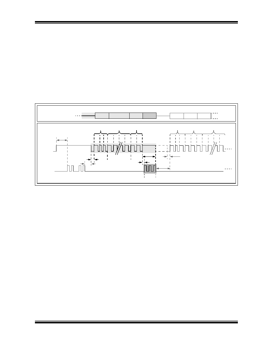
2002 Microchip Technology Inc.
Preliminary
DS40035C-page 25
HCS473
3.2.3.2
PRESENT TRANSPORT CODE
Prior to modifying the device EEPROM, the correct 32-
bit transport code (password) must be presented to
gain write access. This is done with the PRESENT
TRANSPORT CODE command followed by the 32-bit
transport code and CRC calculated on the 3-bit com-
mand and 32 bits of data.
The HCS473 will return an Acknowledge if the trans-
port code matches the value programmed in produc-
tion; write access has been granted.
The next command (usually a write) must begin T
CMD
after the Acknowledge, Figure 3-13.
The present transport code sequence must precede a
write sequence but not necessarily immediately. Per-
haps all four user memory locations will be written and
verified. The present transport code sequence must
precede only the first write to gain write access. The
system may then alternately write and read (verify)
multiple memory locations. Write access remains until
the next time the device returns to Low Power mode -
communication error or T
CMD
time out without receiving
another command.
FIGURE 3-13:
PRESENT TRANSPORT CODE SEQUENCE (RF RESPONSE EXAMPLE)
T
SF
ACK
CMD
TCODE
T
CMD
`001
2
'
CRC
2 bits
32 bits
`1'
`0' `0'
LSb
Command
MSb
CRC0
CRC1
CRC
bit0
bit1
32-Bit
bit31
Transport
MSb
LSb
ACK
Transport ACK
T
TPACK
bit30
CMD
ADR
DATA
T
CMD
WRITE Sequence
`1'
`0'
`1'
bi
t0
bi
t1
bi
t2
Address
Command
bit0
bit1
16-Bit
bit15
Write Data
bit14
T
CMD
Write
Wake Sequence
or
Previous Command
Response
Inductive In
(LC Pins)
RF Response
(DATA Pin)
T
CMD
T
CMD
5 LF
TE
T
CMD
T
FINH
MSb
LSb
HCS473
DS40035C-page 26
Preliminary
2002 Microchip Technology Inc.
3.2.3.3
IFF CHALLENGE AND RESPONSE
The HCS473 can perform a 16-bit or 32-bit challenge
and response (IFF) based on the K
EE
L
OQ
encryption
algorithm.
The transponder reader follows the 3-bit IFF command
with one of four possible options indicating a 16 or 32-
bit challenge and whether to use the encoder or tran-
sponder crypto key to create the response (Table 3-5).
The 3-bit option is followed by the appropriate 16 or 32-
bit challenge; typically a random number. The
sequence ends with a CRC calculated over the com-
mand, option and challenge bits, (Figure 3-14).
The HCS473 encrypts the challenge using the desig-
nated crypto key and responds with a 32-bit result. The
reader authenticates the response by decrypting it and
verifying it matches the original challenge.
If 16-bit IFF is selected, the 32-bit response consists of
two copies of the 16-bit challenge.
RFRSP determines if the response will be transmitted
on the DATA pin. If enabled, the response will follow the
selected Encoder mode code hopping format with the
hopping code replaced with the 32-bit response. The
transmissions will contain a button code of `0000'.
LFRSP determines if the response will be transmitted
on the LC pins. The LC pin response will be the 32-bit
result, modulated PPM format.
If both RFRSP and LFRSP are enabled, the HCS473
will send the response on the DATA pin immediately fol-
lowed by the PPM response on the LC pins. Refer to
Section 3.2.1.7 for further response path details.
The next command must begin T
CMD
after the
response.
FIGURE 3-14:
IFF SEQUENCE (RF RESPONSE EXAMPLE)
T
SF
ACK
CMD
OPT
CHAL
T
CMD
`010
2
' 3 bits
16/32
CRC
2 bits
T
IFF
RESPONSE
bits
`0'
`1'
`0'
bit0
bit1
LSb
MS
b
bit2
Option
Command
MS
b
LSb
CRC0
CRC1
CRC
T
FINH
Preamble
Header
IFF Response
(32 bit
s)
Fixe
d Cod
e
T
IFF
RF Response (RFRSP=1)
bit0
bit1
16/32-Bit
bit15/31
Challenge
MS
b
LSb
Optional Next
Command
T
CMD
LF must remain on if following
with consecutive command
Wake Sequence
or
Previous Command
Response
Inductive In
(LC Pins)
RF Response
(DATA Pin)
T
CMD
T
CMD
or if waiting for LF response
MS
b
LSb

2002 Microchip Technology Inc.
Preliminary
DS40035C-page 27
HCS473
3.2.3.4
READ Command
The transponder reader follows the 3-bit READ com-
mand with one of eight possible 3-bit address options
indicating which 16-bit EEPROM word to retrieve
(Table 3-5) and a 2-bit CRC calculated over the com-
mand and address bits.
The HCS473 retrieves the data and returns the 16-bit
response by creating a 32-bit value containing two cop-
ies of the response (Figure 3-15).
RFRSP determines if the response will be transmitted
on the DATA pin. If enabled, the response will follow the
selected Encoder mode code hopping format with the
hopping code replaced with the 32-bit response. The
transmissions will contain a button code of `0000'.
LFRSP determines if the response will be transmitted
on the LC pins. The LC pin response will be the 32-bit
result, modulated PPM format.
If both RFRSP and LFRSP are enabled, the HCS473
will send the response on the DATA pin immediately fol-
lowed by the PPM response on the LC pins. Refer to
Section 3.2.1.7 for further response path details.
The following locations are available to read:
� The 64-bit general purpose user EEPROM.
� The 32-bit serial number. The serial number is
also transmitted in each code hopping transmis-
sion.
� The16-bit device identifiers #1 and #2.
The next command must begin T
CMD
after the read
response.
FIGURE 3-15:
READ SEQUENCE (RF RESPONSE EXAMPLE)
T
SF
ACK
CMD
ADR
CRC
T
CMD
`100
2
'
3 bits 2 bits
T
READ
RESPONSE
`0'
`0'
`1'
bit0
bit1
LSb
MSb
bit2
Address
Command
MSb
LSb
CRC0
CRC1
CRC
T
FINH
Preamble
Header
Read Dat
a
(32 bit
s)
Fixed Code
T
READ
RF Response
Inductive In
RF Response (RFRSP=1)
Wake Sequence
or
Previous Command
Response
Optional Next
Command
T
CMD
bit0
bit1
bit2
Next
Command
T
CMD
T
CMD
(LC Pins)
(DATA Pin)
T
CMD
T
CMD
LF must remain on if following
with consecutive command
or if waiting for LF response
MSb
LSb
HCS473
DS40035C-page 28
Preliminary
2002 Microchip Technology Inc.
3.2.3.5
WRITE Command
The transponder reader follows the 3-bit WRITE com-
mand with one of eight possible 3-bit address options
indicating which 16-bit EEPROM word to write to
(Table 3-5) and a 2-bit CRC calculated over the com-
mand, address and data bits.
The HCS473 will attempt to write the value into
EEPROM, responding with an Acknowledge sequence
if successful (Figure 3-15).
The following locations are available to write:
� The 64-bit general purpose user EEPROM.
� The 32-bit serial number.
� The16-bit Device Identifiers #1 and #2.
A Transport Code, write access password, protects the
memory locations from undesired modification. The
reader must precede the Write sequence with a suc-
cessful PRESENT TRANSPORT CODE sequence.
Only a correct match with the transport code pro-
grammed during production will allow write access to
the memory locations.
The next command must begin T
CMD
after the write
Acknowledge.
The PRESENT TRANSPORT CODE sequence must
precede a WRITE sequence but not necessarily imme-
diately. Perhaps all four user memory locations will be
written and verified. The PRESENT TRANSPORT
CODE sequence must precede only the first write. The
system may then alternately write and read (verify)
multiple memory locations. Write access status
remains until the next time the device returns to sleep -
communication error or T
CMD
without receiving another
command.
FIGURE 3-16:
WRITE SEQUENCE (RF RESPONSE EXAMPLE)
T
CMD
bit0
bit1
bit2
Next
Command
T
CMD
Inductive In
(LC Pins)
CMD
ADR
DATA
T
CMD
`101
2
'
3 bits 16 bits
ACK
CRC
2 bits
T
WRT
`1'
`0'
`1'
bit0
bit1
LSb
MSb
bit2
Address
Command
MSb
LSb
CRC0
CRC1
CRC
T
FINH
T
WRT
Write ACK
bit0
bit1
16-Bit
bit15
Write Data
MSb
LSb
bit14
Optional Next
Command
T
CMD
T
CMD
RF Response
(DATA Pin)
T
CMD
LF must remain on if following
with consecutive command
or if waiting for LF response
5 LF
TE
Sequence
Previous Command
Sequence
Previous Command
MSb
LSb
2002 Microchip Technology Inc.
Preliminary
DS40035C-page 29
HCS473
3.2.3.6
REQUEST HOPPING CODE
COMMAND
The REQUEST HOPPING CODE command tells the
HCS473 to increment the synchronization counter and
build the 32-bit code hopping portion of the encoder
code word.
A delay of T
HOP
occurs while the HCS473 increments
the counter (updating EEPROM values) and encrypts
the response.
RFRSP determines if the response will be transmitted
on the DATA pin. If enabled, the response will be a sin-
gle K
EE
L
OQ
code hopping code word, based on
Encoder mode options. The code word will contain a
button code of `0000
2
', indicating the transmission did
not result from a button press.
LFRSP determines if the response will be transmitted
on the LC pins. The LC pin response will be the 32-bit
hopping portion of the code word, modulated PPM for-
mat.
If both RFRSP and LFRSP are enabled, the HCS473
will send the response on the DATA pin immediately fol-
lowed by the PPM response on the LC pins. Refer to
Section 3.2.1.7 for further response path details.
The next command must begin T
CMD
after the code
hopping response.
FIGURE 3-17:
REQUEST HOPPING CODE SEQUENCE (RF RESPONSE EXAMPLE)
Fixed Code
T
SF
ACK
CMD
CRC
T
CMD
`110
2
'
2 bits
T
HOP
RESPONSE
`0'
`1'
`1'
LSb
Command
MS
b
CRC0
CRC1
CRC
T
FINH
Preamble
Header
Hop Code
(32 bit
s)
T
HOP
RF Response (RFRSP=1)
Optional Next
Command
T
CMD
bit0
bit1
bit2
Next
Command
T
CMD
T
CMD
Inductive In
(LC Pins)
RF Response
(DATA Pin)
T
CMD
T
CMD
LF must remain on if following
with consecutive command
or if waiting for LF response
Wake Sequence
or
Previous Command
Response
MS
b
LSb
HCS473
DS40035C-page 30
Preliminary
2002 Microchip Technology Inc.
3.2.3.7
ANTI-COLLISION OFF
Anticollision is enabled/disabled for a given device by
the ACOL configuration option. The ANTICOLLISION
OFF command may be used to temporarily bypass
anticollision requirements for a single communication
sequence. It allows communication to an anticollision
enabled HCS473 if the VID and TID are not known
(perhaps during a learning sequence).
The command must immediately follow the wake-up
sequence, Figure 3-18. The HCS473 acknowledges
the command receipt, then reacts to all commands
even if the anticollision (ACOL) configuration option is
enabled and a SELECT TRANSPONDER sequence
has not been performed.
The next command must begin T
CMD
after the
Acknowledge.
The HCS473 remains in this anticollision off state until
the next time the device returns to SLEEP - communi-
cation error or T
CMD
without receiving another com-
mand. Multiple commands may therefore be sent
without sending the ANTICOLLISION OFF command
prior to each command.
FIGURE 3-18:
ANTICOLLISION OFF SEQUENCE (RF RESPONSE EXAMPLE)
3.2.4
LF RESPONSE CONSIDERATIONS
As LF responses are transmitted by the HCS473 plac-
ing a short across the LC antenna inputs, dissipating
the antenna resonance, the transponder reader must
still be sending the 125 kHz field for LF responses to
work. The low frequency field on-time (T
FINH
) must
therefore be approriately adjusted to receive an LF
Acknowledge sequence or LF data response, Figure 3-
19 and Figure 3-20.
3.2.5
CONSECUTIVE COMMAND
CONSIDERATIONS
Transponder commands may consecutively follow one
another to minimize communication time as the wake-
up sequence, device selection, anticollision off and
transport code presentation need not be repeated for
every command.
Consideration must be given to how long the transpon-
der reader keeps the LF signal on after the last data
bit's rising edge (T
FINH
) when a command sequence...
� will be followed by another command sequence
� will result in a LF response
The reason is that the HCS473's analog LF antenna
input circuitry will return to Low-power mode when the
125 kHz field remains absent; requiring a new wake-up
sequence to continue communication.
The HCS473's analog section will never return to Low-
power mode during any T
CMD
window waiting for an LC
input communication edge, so long as the LF signal
existed up to the beginning of the T
CMD
window.
Please refer to Figure 3-19 and Figure 3-20 for exam-
ples on adjusting T
FINH
for consecutive commands and
LF responses.
3.2.6
LF COMMUNICATION ANALOG
DELAYS
LF communication edge delays result from the
HCS473's internal analog circuit as well as the external
LC resonant antennas, Figure 3-21.
The rising and falling edge delays inherent to the
HCS473's internal filtering are known and specified in
Table 7-5, T
FILTR
and T
FILTF
.
The cumulative rising and falling edge delays inherent
to both the series LC transmitting antenna and parallel
LC receiving antennas are design dependent, not a
HCS473 specification.
CMD
CRC
T
CMD
`111
2
'
2 bits
T
CMD
`1'
`1'
`1'
LSb
Command
MSb
CRC0
CRC1
CRC
ACK
T
FINH
ACOL Off ACK
T
AOACK
WAKE ACK
CMD
`XXX'
bit0
bit1
bit2
Next
Command
T
CMD
Inductive In
(LC Pins)
T
SF
ACK
RF Response
(DATA Pin)
T
CMD
T
CMD
5 LF
TE
T
CMD
Next
Command
MSb
LSb
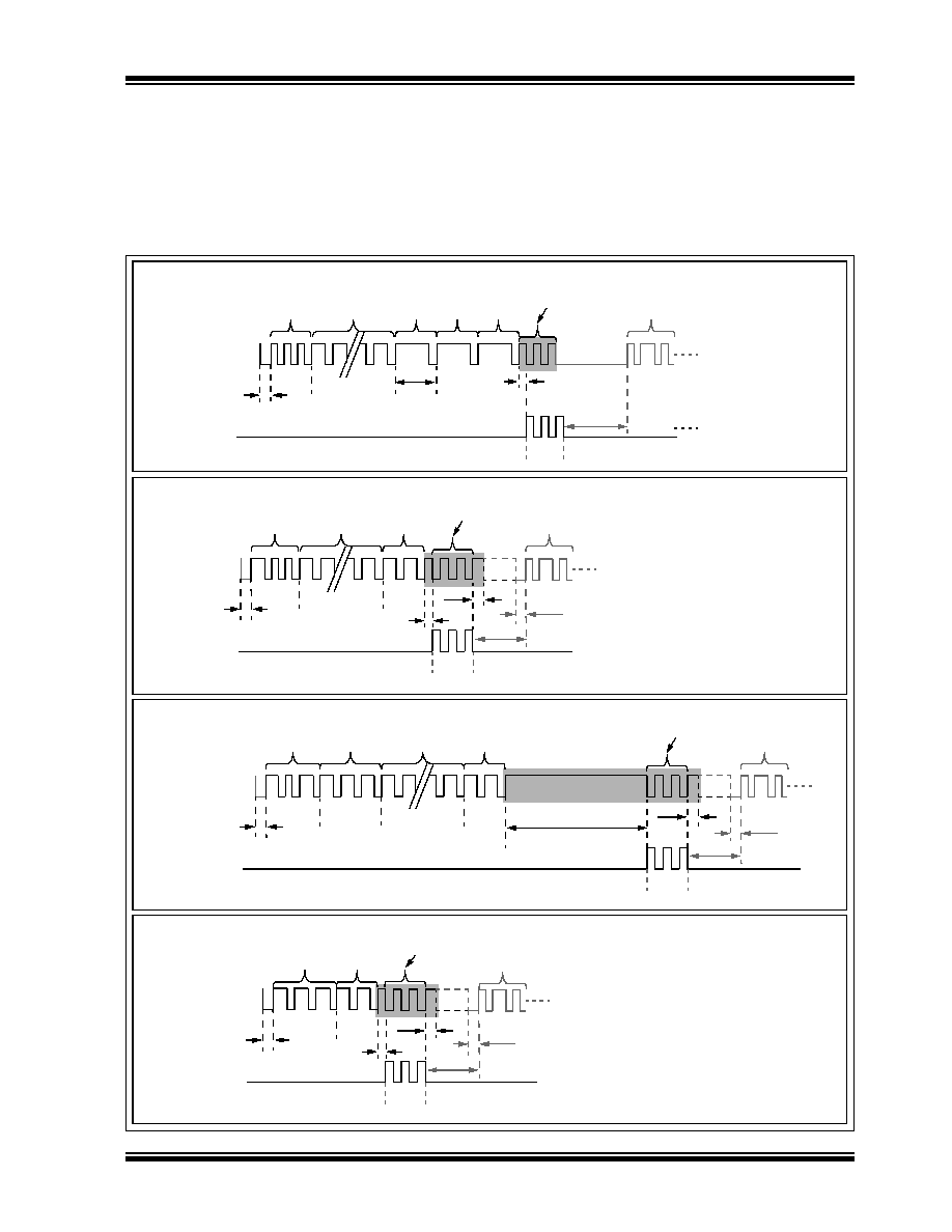
2002 Microchip Technology Inc.
Preliminary
DS40035C-page 31
HCS473
Table 7-5 timing values are compensated only for
HCS473 internal filter delays. The transponder reader
designer must compensate communication timing
accordingly for the cumulative antenna delays.
Use LF Demodulator mode to see the effects of the
internal filters and the LC antennae, Section 3.2.1.2.
It must be clearly understood that the HCS473 core
does not see the LF field immediately upon the base
station turning it on, nor does it immediately detect its
removal. If the internal analog delay and cumulative
antenna delays are greater than a given low time, the
HCS473 will obviously never "see" the low.
FIGURE 3-19:
LF ACK RESPONSE ADJUSTMENTS (LFRSP=1)
T
AOACK
LSb
Command
MS
b
CRC
MS
b
LSb
Transport ACK
T
TPACK
Inductive
(LC Pins)
RF Response
(DATA Pin)
T
CMD
Present Transport Code Sequence
Inductive
(LC Pins)
LSb
MS
b
Address
Command
MS
b
LSb
CRC
T
WRT
Write ACK
16-Bit
Write Data
MS
b
LSb
RF Response
(DATA Pin)
T
CMD
Write Sequence
LSb
Command
MSb
CRC
ACOL Off ACK
Inductive
(LC Pins)
RF Response
(DATA Pin)
T
CMD
32-Bit
Transport
Anticollision Off Sequence
T
FINH
T
FINH
T
FINH
Next
Command
T
CMD
Next
Command
T
CMD
Next
Command
T
CMD
5 LF
TE
5 LF
TE
5 LF
TE
T
CMD
T
CMD
T
CMD
Simultaneous
LF ACK
Simultaneous
LF ACK
Simultaneous
LF ACK
Transponder Select Sequence
LSb
Command
MSb
TID=0
12-Bit
VID
MSb
LSb
Transponder Select ACK
TID=1
TID=2
6 LF
TE
T
TSCMD
Next
Command
T
TSACK
Inductive
(LC Pins)
RF Response
(DATA Pin)
T
CMD
Simultaneous
LF ACK
MSb
LSb
MSb
LSb
MS
b
LSb
5 LF
TE
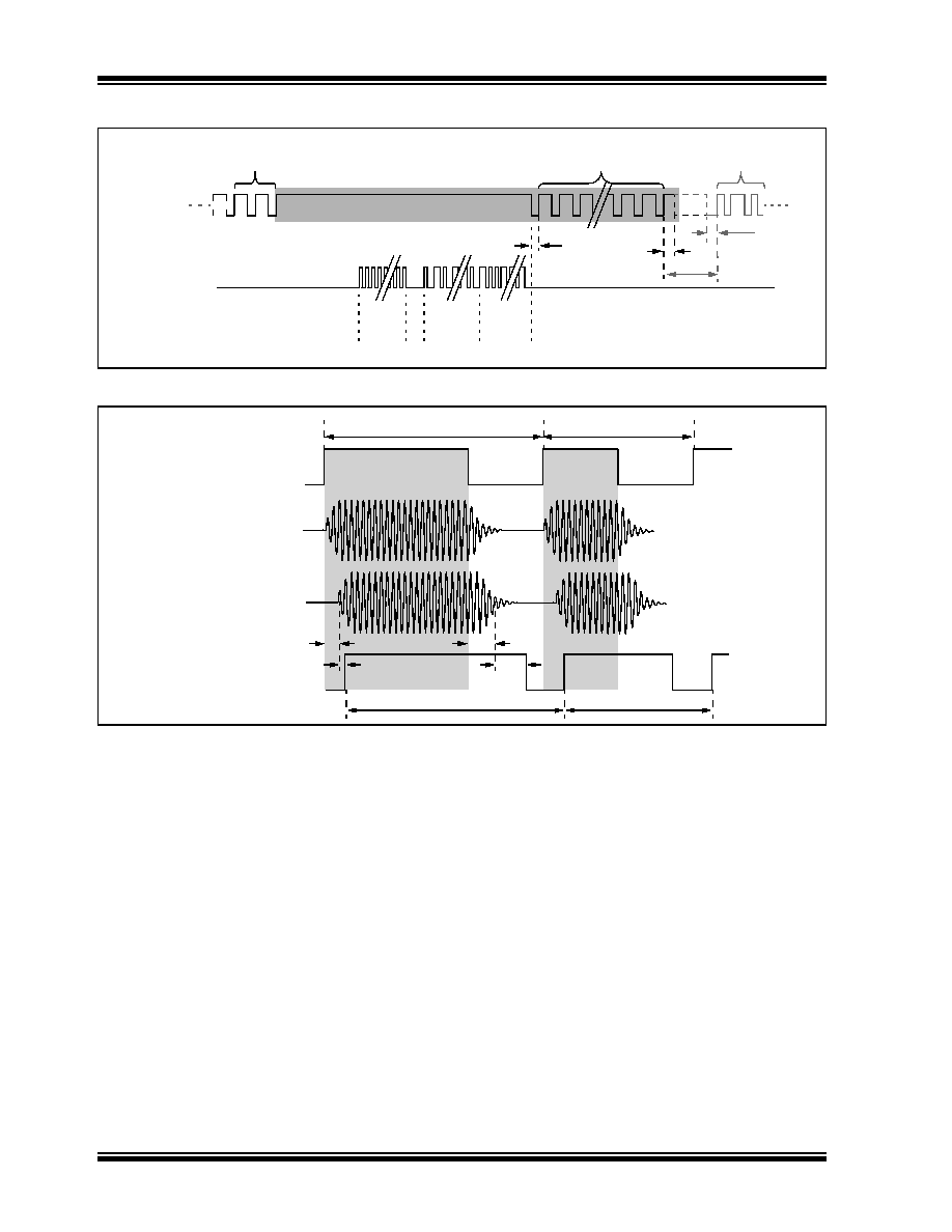
HCS473
DS40035C-page 32
Preliminary
2002 Microchip Technology Inc.
FIGURE 3-20:
LF DATA RESPONSE ADJUSTMENTS (LFRSP=1)
FIGURE 3-21:
LF COMMUNICATION ANALOG DELAYS
3.2.7
RECEIVE STABILITY -
CALCULATING COMMUNICATION
T
E
The HCS473's internal oscillator may vary �10% over
the device's rated voltage and temperature range for
commercial temperature devices. A certain percentage
of industrial temperature devices vary further on the
slow side, -20%, when used at higher voltages (V
DD
>
3.5V) and cold temperature. When the internal oscilla-
tor varies, both its transmitted T
E
and expected T
E
when receiving will vary.
The HCS473 receive capability is ensured over a �10%
oscillator variance, with receive capability no longer
robust as oscillator variance approaches �15%. Indus-
trial devices operating at V
DD
voltages greater than
3.5V (and cold temperature) are therefore not guaran-
teed to be able to properly receive when communicated
to using an exact T
E
. When designing for these specific
operating conditions, the system designer must imple-
ment a method to adjust communication timing to the
speed of the HCS473.
Communication reliability with the transponder may be
improved by the transponder reader calculating the
HCS473's T
E
from the Field Acknowledge sequence
and using this exact time element in communication to
and in reception routines from the transponder.
Always begin and end the time measurement on rising
edges. Whether LF or RF, the falling edge decay rates
may vary but the rising edge relationships should
remain consistent. A common T
E
calculation method
would be to time an 8T
E
sequence from the first Field
Acknowledge, then divide the value down to determine
the single T
E
value. An 8 T
E
measurement will give
good resolution and may be easily right-shifted (divide
by 2) three times for the math portion of the calculation
(Figure 3-22).
IFF, Read and Request Hop
CRC
Preamble
Header
Response
(32 bit
s)
Fixed Code
(37 bit
s
)
RF Response (RFRSP=1)
Inductive
(LC Pins)
RF Response
(DATA Pin)
MSb
LSb
32-Bit LF Response (LFRSP=1)
T
FINH
1 LF
TE
Next
Command
T
CMD
T
CMD
Resulting 125 kHz on
Transponder Reader
Digital Representation
of Communication from
Transponder Reader
Antenna (TX)
600
�s
400
�s
Resulting 125 kHz on
Transponder Card
Antenna (RX)
Resulting digital signal
processed by HCS473,
after analog filter
600
�s
400
�s
T
FILTR
T
FILTF
T
ANTR
T
ANTF
Bit `1', 200
�s LF
TE
Bit `0', 200
�s LF
TE
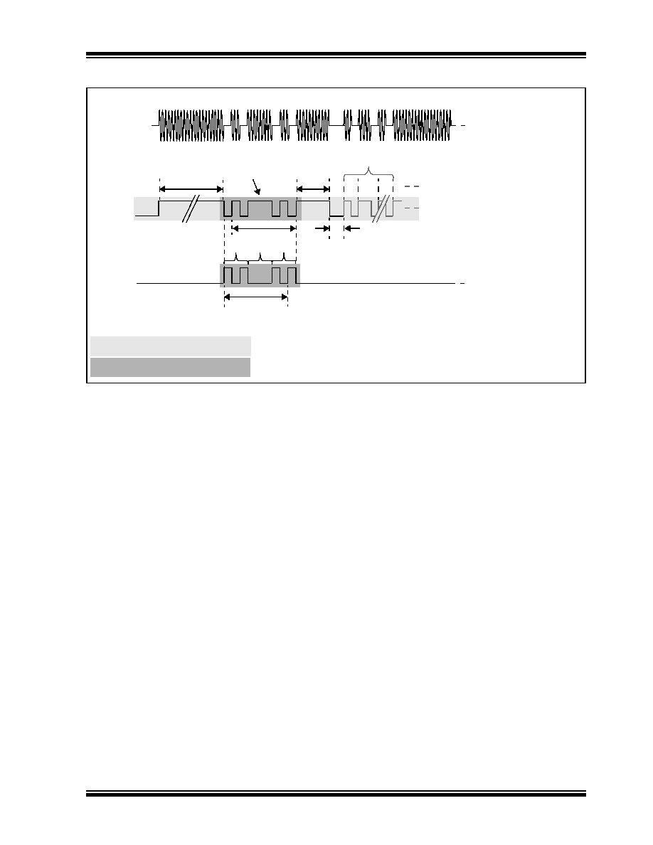
2002 Microchip Technology Inc.
Preliminary
DS40035C-page 33
HCS473
FIGURE 3-22:
Calculating Communication T
E
3.2.8
RFEN DURING LF
COMMUNICATION (Figure 3-23)
3.2.8.1
Wake-up Sequence
The wake-up Acknowledge sequence has the shortest,
but fixed, PLL setup time, 1LF
TE
.
3.2.8.2
Transponder Select Sequence
PLL setup occurs on the rising edge of the first VID bit
in anticipation of the TID Acknowledge. The setup time
before the ACK begins is therefore a function of...
� LF baud rate
� VID value
� TID value
3.2.8.3
ACK Response Sequences
Concluding with CRC
Command sequences ending with CRC bits and
expecting an Acknowledge response have a similar
PLL setup sequence. This includes "Present Transport
Code", "Write" and "Anticollision Off".
PLL setup occurs on the rising edge of the first CRC bit
in anticipation of the Acknowledge. The setup time is
therefore a function of...
� LF baud rate
� CRC value
� Response time: T
TPACK
, T
WRT
, T
AOACK
.
3.2.8.4
Data Response Sequences
Concluding with CRC
Command sequences ending with CRC bits and
expecting data response (code hopping word) have a
similar PLL setup sequence. This includes "IFF",
"Read" and "Request Hopping Code".
PLL setup occurs on the rising edge of the first CRC bit
in anticipation of the data transmission. The setup time
is therefore a function of...
� LF baud rate
� CRC value
� Response time: T
IFF
, T
READ
, T
HOP
.
Communication from reader to HCS473
Communication from HCS473 to reader
8LF
TE
8LF
TE
T
SF
Command
T
CMD
SKIPACK = 0 - Field Acknowledge sent when device wakes
Inductive
(LC)
RF
Response
(DATA)
125 kHz Field
(on LC pins)
T
CMD
bit0
bit1
bit2
3LF
TE
3LF
TE
3LF
TE
3LF
TE
Simultaneous LF
Acknowledge
(LFRSP=1)
RF Acknowledge
(RFRSP=1)
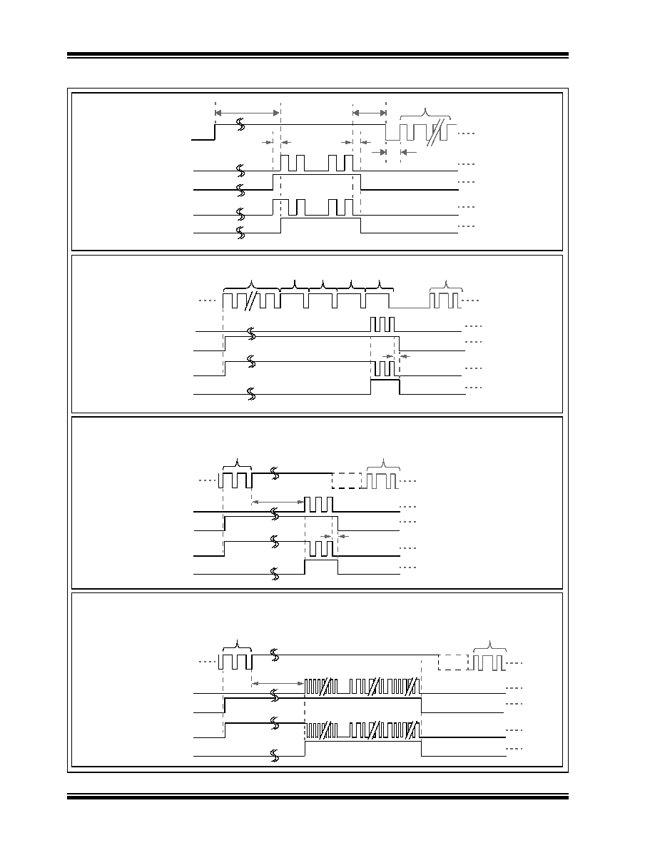
HCS473
DS40035C-page 34
Preliminary
2002 Microchip Technology Inc.
FIGURE 3-23:
RFEN BEHAVIOR DURING LF COMMUNICATION
ACK Response Sequences Concluding with CRC
Data Response Sequences Concluding with CRC
Transponder Select Sequence
- Present Transport Code
- Write
- Anticollision Off
- IFF
- Read
- Request Hopping Code
CRC
Response
Command
Inductive In (LC)
RF (DATA)
PLL (RFEN)
RF (DATA)
PLL (RFEN)
ASK
FSK
1 LF
TE
CRC
Command
RF (DATA)
PLL (RFEN)
RF (DATA)
PLL (RFEN)
ASK
FSK
Inductive In (LC)
TID=0
12-Bit VID
TID=1
TID=2
TID=3
Next
Command
RF (DATA)
PLL (RFEN)
RF (DATA)
PLL (RFEN)
ASK
FSK
Inductive In (LC)
1 LF
TE
Time
Response
Time
T
SF
Command
T
CMD
Inductive In (LC)
RF (DATA)
T
CMD
Wake-up Sequence
PLL (RFEN)
RF (DATA)
PLL (RFEN)
ASK
FSK
1 LF
TE
1 LF
TE
2002 Microchip Technology Inc.
Preliminary
DS40035C-page 35
HCS473
3.3
CONFIGURATION SUMMARY
TABLE 3-6:
CONFIGURATION SUMMARY
Symbol
Address: Bits
Description
(1)
Reference
Section
USR 0
00:
16 bits
User EEPROM Area
3.2.3.4,
3.2.3.5
USR 1
02:
16 bits
User EEPROM Area
USR 2
04:
16 bits
User EEPROM Area
USR 3
06:
16 bits
User EEPROM Area
SER
08:
32 bits
Encoder Serial Number
DEVID 1
0C:
16 bits
Device Identifier #1 - Vehicle/Token ID Number #1
3.2.1.4
DEVID 2
0E:
16 bits
Device Identifier #2 - Vehicle/Token ID Number #2
IFF KEY
10:
64 bits
IFF Key
3.2.3.3
COUNT
18:
64 bits
Encoder Synchronization Counter and Checksum
1.2.3
KEY
20:
64 bits
Encoder Key
SEED
28:
60 bits
Encoder Seed Value
3.1.2.2
TCODE
30:
32 bits
Transport Code
3.2.3.2
DISC
34:
10 bits
Encoder Discrimination Value
3.1.8
RFEN
36: 7 - - - - - - - RF Enable Pin
0 - S3
1 - RF Enable
3.1.4.8
PLLSEL
36: - 6 - - - - - - PLL Interface Select
0 - ASK
1 - FSK
3.1.4.7
VLOWSEL
36: - - 5 - - - - - Low Voltage Trip Point Select
( 2)
0 - 2.2V
1 - 3.3V
3.1.4.6
CNTSEL
36: - - - 4 - - - - Counter Select
0 - 16 bits
1 - 20 bits
3.1.4.5
QUEN
36: - - - - 3 - - - Queue Counter Enable
0 - Disable
1 - Enable
3.1.4.4
XSER
36: - - - - - 2 - - Extended Serial Number
0 - 28 bits
1 - 32 bits
3.1.4.3
HSEL
36: - - - - - - 1 - Header Select
( 1)
0 - 4 TE
1 - 10 TE
3.1.4.2
MSEL
36: - - - - - - - 0 Modulation Format
0 - PWM
1 - Manchester
3.1.4.1
SDMD
37: 7 - - - - - - - Seed Mode
0 - User
1 - Production
3.1.4.12
SDLM
37: - 6 - - - - - - Limited Seed
0 - Unlimited
1 - Limited
3.1.4.11
SDTM
37: - - 5 4 - - - - Time Before Seed code word
( 1)
Value
Time (s)
3.1.4.10
00
2
0.0
01
2
0.8
10
2
1.6
11
2
3.2
SDBT
37: - - - - 3 2 1 0 Seed Button Code
Bit order = S3-S2-S1-S0
3.1.4.9
TSEL
38: 7 6 - - - - - - Timeout Select
( 1)
Value
Time (s)
3.1.4.16
00
2
4
01
2
8
10
2
16
11
2
32
MTX
38: - - 5 4 - - - - Minimum Code Words
Value
Value
3.1.4.15
00
2
1
01
2
2
10
2
4
11
2
8
HCS473
DS40035C-page 36
Preliminary
2002 Microchip Technology Inc.
GSEL
38: - - - - 3 2 - - Guard Time Select
( 1)
Value
Time (ms)
3.1.4.14
00
2
0.0
01
2
6.4
10
2
51.2
11
2
102.4
RFBSL
38: - - - - - - 1 0 RF Transmission Baud Rate
Select
( 1)
Value
TE (�s)
3.1.4.13
00
2
100
01
2
200
10
2
400
11
2
800
LFDEMOD
39: 7 - - - - - - - LF Demodulator
0 - Normal
1 - Demod
3.2.1.2
TPLS
39: - - - - 3 - - - Transponder Preamble Length
0 - Normal
1 - Short
3.2.1.1
PRD
39: - - - - - 2 - - Preamble Duty Cycle
( 1)
0 - 33%
1 - 50%
3.1.4.19
LPRL
39: - - - - - - 1 - Long Preamble Length
( 1)
0 - 75ms
1 - 100ms 3.1.4.18
LPRE
39: - - - - - - - 0 Long Preamble Enable
0 - Disable
1 - Enable
3.1.4.17
SKIPACK
3A: 7 - - - - - - - Skip First ACK
0 - Disable
1 - Enable
3.2.1.8
RFRSP
3A: - 6 - - - - - - RF Response
0 - Disable
1 - Enable
3.2.1.7
LCRSP
3A: - - 5 - - - - - LC Response
0 - Disable
1 - Enable
3.2.1.7
DAMP
3A: - - - 4 - - - - Intelligent LC Damping
0 - Disable
1 - Enable
3.2.1.6
PXMA
3A: - - - - 3 - - - Proximity Activation
0 - Disable
1 - Enable
3.2.1.5
ACOL
3A: - - - - - 2 - - Anticollision
0 - Disable
1 - Enable
3.2.1.4
LFBSL
3A: - - - - - - 1 0 LF Transmission Baud Rate
Select
( 1)
Value
TE (�s)
3.2.1.3
00
2
100
01
2
200
10
2
400
11
2
800
END
3F
01011010
Unused, always set = 5A
Note 1: All Timing values vary �10%. Industrial temperature devices operating at cold and 3.5V < V
DD
< 5.5V vary
+10%, -20%.
2: Voltage thresholds should be �250 mV for the low voltage range and �400 mV for the high voltage range.
TABLE 3-6:
CONFIGURATION SUMMARY
Symbol
Address: Bits
Description
(1)
Reference
Section

2002 Microchip Technology Inc.
Preliminary
DS40035C-page 37
HCS473
4.0
PROGRAMMING
SPECIFICATION
The HCS473 programming specification is extensively
covered in document DS41163 and will not be dupli-
cated here.

HCS473
DS40035C-page 38
Preliminary
2002 Microchip Technology Inc.
NOTES:
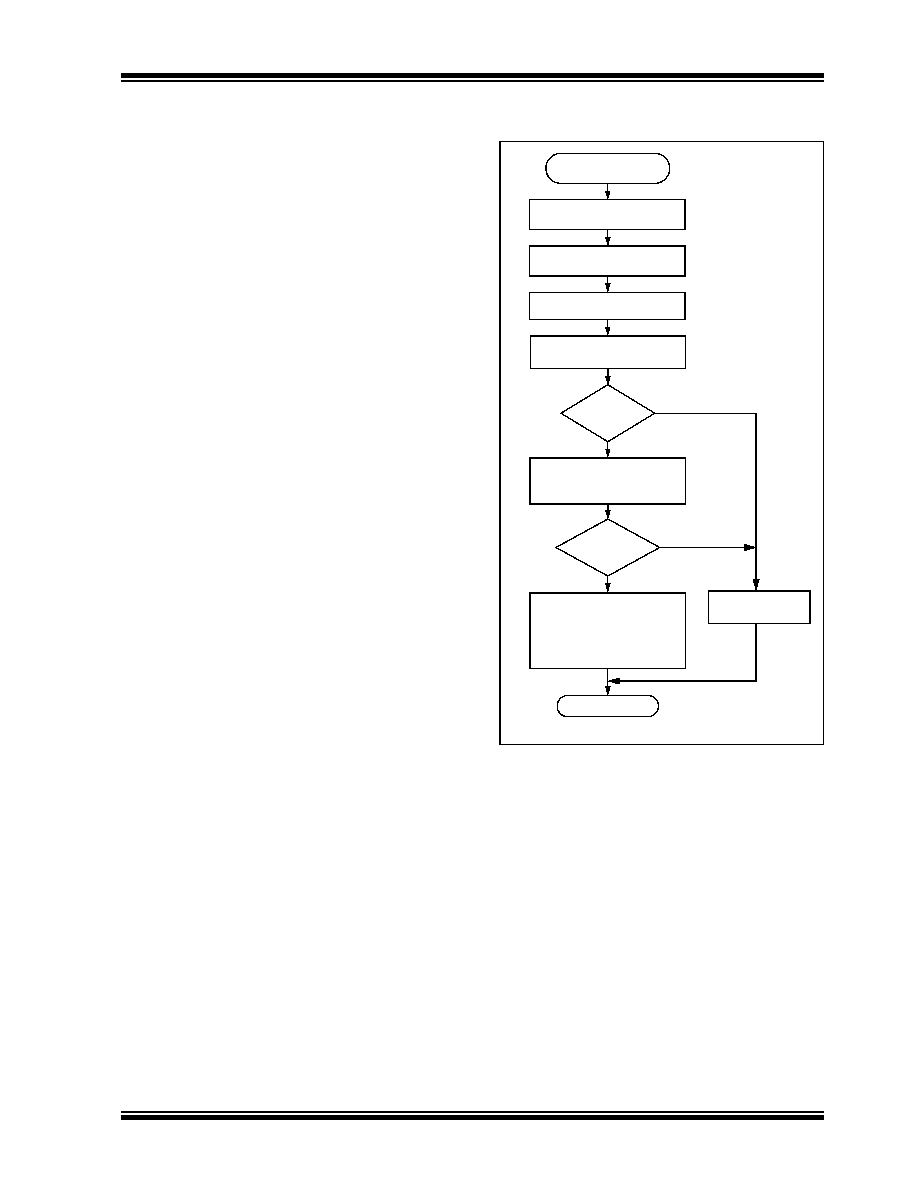
2002 Microchip Technology Inc.
Preliminary
DS40035C-page 39
HCS473
5.0
INTEGRATING THE HCS473
INTO A SYSTEM
Use of the HCS473 in a system requires a compatible
decoder. This decoder is typically a microcontroller with
a low frequency coil antenna and radio frequency
receiver. Example firmware routines that accept and
decrypt K
EE
L
OQ
transmissions can be found in Applica-
tion Notes and the K
EE
L
OQ
license disk.
5.1
Training the Receiver
In order for a transmitter to be used with a decoder, the
transmitter must first be `learned'. When a decoder
learns a transmitter, it is suggested that the decoder
stores the serial number and current synchronization
value in EEPROM. Some learning strategies have
been patented and care must be taken not to infringe
on them. The decoder must keep track of these values
for every transmitter that is learned (see Figure 5-1).
The maximum number of transmitters that can be
learned is limited only by the available EEPROM
memory. The decoder must also store the manufac-
turer's code in order to learn a transmitter. This value
will not change in a typical system, so it is usually
stored as part of the microcontroller ROM code. Storing
the manufacturer's code as part of the ROM code
improves security by keeping it off the external bus to
the EEPROM.
FIGURE 5-1:
TYPICAL LEARN
SEQUENCE
5.2
Decoder Operation
In a typical decoder operation (Figure 5-2), the key
generation on the decoder side is performed by taking
the serial number from a transmission and combining
that with the manufacturer's code to create the same
secret key that was used by the transmitter. Once the
secret key is obtained, the rest of the transmission can
be decrypted. The decoder waits for a transmission
and immediately can check the serial number to
determine if it is a learned transmitter. If it is, the
encrypted portion of the transmission is decrypted
using the stored key. It uses the discrimination bits to
determine if the decryption was valid. If everything up
to this point is valid, the synchronization value
is evaluated.
Enter Learn
Mode
Wait for Reception
of a Valid Code & Seed
Generate Key
Use Generated Key
to Decrypt
Compare Discrimination
Value with Fixed Value
Equal
Wait for Reception
of Second Valid Code
Counters
Sequential
?
?
Exit
Learn
Unsuccessful
No
No
Yes
Yes
(Optional)
Learn Successful Store:
Serial Number
Encoder Key
Synchronization Counter
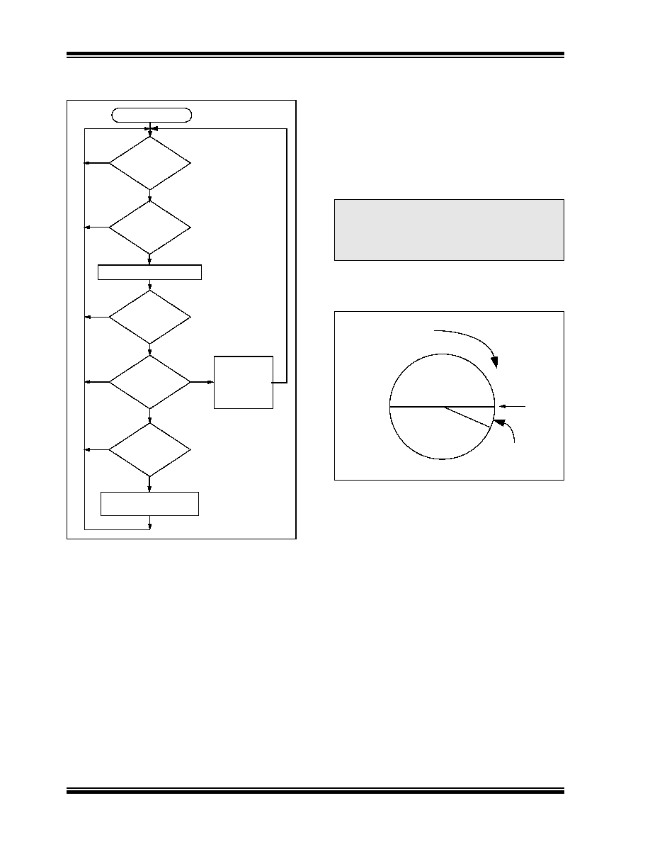
HCS473
DS40035C-page 40
Preliminary
2002 Microchip Technology Inc.
FIGURE 5-2:
TYPICAL DECODER
OPERATION
5.3
Synchronization with Decoder
The technology features a sophisticated
synchronization technique (Figure 5-3) which does not
require the calculation and storage of future codes. If
the stored counter value for that particular transmitter
and the counter value that was just decrypted are
within a window of 16 codes, the counter is stored and
the command is executed. If the counter value was not
within the single operation window, but is within the
double operation window of 32K codes (when using a
16-bit counter), the transmitted synchronization value
is stored in temporary location and it goes back to wait-
ing for another transmission.
When the next valid transmission is received, it will
check the new value with the one in temporary storage.
If the two values are sequential, it is assumed that the
counter had just gotten out of the single operation `win-
dow'. Since it is now back in sync, the new synchroni-
zation value is stored and the command executed.
If a transmitter has somehow gotten out of the double
operation window, the transmitter will not work and
must be relearned. Since the entire window rotates
after each valid transmission, codes that have been
used are part of the `blocked' (32K) codes and are no
longer valid. This eliminates the possibility of grabbing
a previous code and retransmitting to gain entry.
FIGURE 5-3:
SYNCHRONIZATION
WINDOW (16-BIT
COUNTER)
5.4
Inductive Communication
Communication between a base station and a HCS473
transponder occurs via magnetic coupling between the
transponder coil and base station coil. The base station
coil forms part of a series RLC circuit. The base station
communicates to the transponder by switching the 125
kHz signal to the series RLC circuit on and off. Thus,
the base station magnetic field is switched on and off.
The transponder coil is connected in parallel with a res-
onating capacitor (125 kHz) and the HCS473.
When the transponder is brought into the base station
magnetic field, it magnetically couples with this field
and draws energy from it. This loading effect can be
observed as a decrease in voltage across the base sta-
tion resonating capacitor. The K
EE
L
OQ
transponder
communicates to the base station by "shorting out" its
parallel LC circuit. This detunes the transponder and
removes the load, which is observed as an increase in
voltage across the base station resonating capacitor.
The base station capacitor voltage is the input to the
base station AM demodulator circuit. The demodulator
extracts the transponder data for further processing by
the base station software.
?
Transmission
Received
Does
Serial Number
Match
?
Decrypt Transmission
Is
Decryption
Valid
?
Is
Counter
Within 16
?
Is
Counter
Within 32K
?
Update
Counter
Execute
Command
Save Counter
in Temp Location
Start
No
No
No
No
Yes
Yes
Yes
Yes
Yes
No
and
No
Note:
The synchronization method described in
this section is only a typical implementation
and because it is usually implemented in
firmware, it can be altered to fit the needs
of a particular system
Blocked
Entire Window
rotates to eliminate
use of previously
used codes
Current
Position
(32K Codes)
Double
Operation
(32K Codes)
Single Operation
Window (16 Codes)

2002 Microchip Technology Inc.
Preliminary
DS40035C-page 41
HCS473
5.5
Transponder Design
You must initially decide if a ferrite core or an air core
antenna will be used. There are advantages and disad-
vantages to using each. One advantage of using a fer-
rite core is that the coil can have a larger inductance for
a given volume. Volume will usually be the primary con-
straint as it will need to fit into a:
� key fob
� credit card
� other small package.
First step: choose the transponder coil external dimen-
sions because packaging places large constraints on
antenna design.
Second step: properties of the core, coil windings, as
well as the equivalent load placed across the coil must
be determined. Calculations from the first two steps will
fix the initial coil specification. The initial coil specifica-
tion includes:
� Minimum number of wire turns on the coil
� Wire diameter
� Wire resistance
� Coil inductance
� Required resonating capacitor.
Build the initial coil and take appropriate measure-
ments to determine the coil quality factor. The data
gathered to this point may then be used to calculate an
Optimum Coil Specification.
It is not this data sheet's purpose to present in-depth
details regarding LC antennae and their tuning. Please
refer to "Low Frequency Magnetic Transmitter Design
Application Note", AN232, for appropriate LF antenna
design details.
5.6
Security Considerations
The strength of this security is based on keeping a
secret inside the transmitter that can be verified by
encrypted transmissions to a trained receiver. The
transmitter's secret is the manufacturer's key, not the
encryption algorithm. If that key is compromised, then
a smart transceiver can:
� capture any serial number
� create a valid code word
� trick all receivers trained with that serial number.
The key cannot be read from the EEPROM without
costly die probing, but it can be calculated by brute
force decryption attacks on transmitted code words.
The cost for these attacks should exceed what you
would want to protect.
To protect the security of other receivers with the same
manufacturer's code, you need to use the random seed
for secure learn. It is a second secret that is unique for
each transmitter. It's transmission on a special button
press combination can be disabled if the receiver has
another way to find it, or is limited to the first 127 trans-
missions for the receiver to learn it. This way it is very
unlikely to ever be captured. Now if a manufacturer's
key is compromised, new transmitters can be created.
But without the unique seed, they must be relearned by
the receiver. In the same way, if the transmissions are
decrypted by brute force on a computer, the random
seed hides the manufacturer's key and prevents more
than one transmitter from being compromised.
The length of the code word at these baud rates makes
brute force attacks that guess the hopping code require
years to perform. To make the receiver less susceptible
to this attack, make sure that you test all the bits in the
decrypted code for the correct value. Do not just test
low counter bits for sync and the bit for the button input
of interest.
The main benefit of hopping codes is to prevent the
retransmission of captured code words. This works
very well for code words that the receiver decodes. Its
weakness is if a code is captured when the receiver
misses it, the code may trick the receiver once if it is
used before the next valid transmission. To make the
receiver more secure it could increment the counter on
questionable code word receptions. To make the trans-
mitter more secure it could use separate buttons for
lock and unlock functions. Another way would be to
require two different buttons in sequence to gain
access.
There are other ways to make K
EE
L
OQ
systems more
secure, but these are all trade-offs. You need to find a
balance between:
� Security
� Design effort
� Usability (particularly in failure modes).
For example, if a button sticks or someone plays with
it, the counter should not end up in the blocked code
window, rendering the transmitter useless or requiring
the receiver to relearn the transmitter.
Note:
The exact number of turns may be
tweaked such that a standard value reso-
nant capacitor may be used.
Note:
Microchip also has a confidential Applica-
tion Note on Magnetic Sensors (AN832C).
Contact Microchip for a Non-Disclosure
Agreement in order to obtain this applica-
tion note.

HCS473
DS40035C-page 42
Preliminary
2002 Microchip Technology Inc.
NOTES:

2002 Microchip Technology Inc.
Preliminary
DS40035C-page 43
HCS473
6.0
DEVELOPMENT SUPPORT
The PICmicro
�
microcontrollers are supported with a
full range of hardware and software development tools:
� Integrated Development Environment
- MPLAB
�
IDE Software
� Assemblers/Compilers/Linkers
- MPASM
TM
Assembler
- MPLAB C17 and MPLAB C18 C Compilers
- MPLINK
TM
Object Linker/
MPLIB
TM
Object Librarian
� Simulators
- MPLAB SIM Software Simulator
� Emulators
- MPLAB ICE 2000 In-Circuit Emulator
- ICEPICTM In-Circuit Emulator
� In-Circuit Debugger
- MPLAB ICD
� Device Programmers
- PRO MATE
�
II Universal Device Programmer
- PICSTART
�
Plus Entry-Level Development
Programmer
� Low Cost Demonstration Boards
- PICDEM
TM
1 Demonstration Board
- PICDEM 2 Demonstration Board
- PICDEM
3 Demonstration Board
- PICDEM
17 Demonstration Board
- K
EE
L
OQ
�
Demonstration Board
6.1
MPLAB Integrated Development
Environment Software
The MPLAB IDE software brings an ease of software
development previously unseen in the 8-bit microcon-
troller market. The MPLAB IDE is a Windows
�
-based
application that contains:
� An interface to debugging tools
- simulator
- programmer (sold separately)
- emulator (sold separately)
- in-circuit debugger (sold separately)
� A full-featured editor
� A project manager
� Customizable toolbar and key mapping
� A status bar
� On-line help
The MPLAB IDE allows you to:
� Edit your source files (either assembly or `C')
� One touch assemble (or compile) and download
to PICmicro emulator and simulator tools (auto-
matically updates all project information)
� Debug using:
- source files
- absolute listing file
- machine code
The ability to use MPLAB IDE with multiple debugging
tools allows users to easily switch from the cost-
effective simulator to a full-featured emulator with
minimal retraining.
6.2
MPASM Assembler
The MPASM assembler is a full-featured universal
macro assembler for all PICmicro MCU's.
The MPASM assembler has a command line interface
and a Windows shell. It can be used as a stand-alone
application on a Windows 3.x or greater system, or it
can be used through MPLAB IDE. The MPASM assem-
bler generates relocatable object files for the MPLINK
object linker, Intel
�
standard HEX files, MAP files to
detail memory usage and symbol reference, an abso-
lute LST file that contains source lines and generated
machine code, and a COD file for debugging.
The MPASM assembler features include:
� Integration into MPLAB IDE projects.
� User-defined macros to streamline assembly
code.
� Conditional assembly for multi-purpose source
files.
� Directives that allow complete control over the
assembly process.
6.3
MPLAB C17 and MPLAB C18
C Compilers
The MPLAB C17 and MPLAB C18 Code Development
Systems are complete ANSI `C' compilers for
Microchip's PIC17CXXX and PIC18CXXX family of
microcontrollers, respectively. These compilers provide
powerful integration capabilities and ease of use not
found with other compilers.
For easier source level debugging, the compilers pro-
vide symbol information that is compatible with the
MPLAB IDE memory display.

HCS473
DS40035C-page 44
Preliminary
2002 Microchip Technology Inc.
6.4
MPLINK Object Linker/
MPLIB Object Librarian
The MPLINK object linker combines relocatable
objects created by the MPASM assembler and the
MPLAB C17 and MPLAB C18 C compilers. It can also
link relocatable objects from pre-compiled libraries,
using directives from a linker script.
The MPLIB object librarian is a librarian for pre-
compiled code to be used with the MPLINK object
linker. When a routine from a library is called from
another source file, only the modules that contain that
routine will be linked in with the application. This allows
large libraries to be used efficiently in many different
applications. The MPLIB object librarian manages the
creation and modification of library files.
The MPLINK object linker features include:
� Integration with MPASM assembler and MPLAB
C17 and MPLAB C18 C compilers.
� Allows all memory areas to be defined as sections
to provide link-time flexibility.
The MPLIB object librarian features include:
� Easier linking because single libraries can be
included instead of many smaller files.
� Helps keep code maintainable by grouping
related modules together.
� Allows libraries to be created and modules to be
added, listed, replaced, deleted or extracted.
6.5
MPLAB SIM Software Simulator
The MPLAB SIM software simulator allows code devel-
opment in a PC-hosted environment by simulating the
PICmicro series microcontrollers on an instruction
level. On any given instruction, the data areas can be
examined or modified and stimuli can be applied from
a file, or user-defined key press, to any of the pins. The
execution can be performed in single step, execute
until break, or Trace mode.
The MPLAB SIM simulator fully supports symbolic debug-
ging using the MPLAB C17 and the MPLAB C18 C com-
pilers and the MPASM assembler. The software simulator
offers the flexibility to develop and debug code outside of
the laboratory environment, making it an excellent multi-
project software development tool.
6.6
MPLAB ICE High Performance
Universal In-Circuit Emulator with
MPLAB IDE
The MPLAB ICE universal in-circuit emulator is intended
to provide the product development engineer with a
complete microcontroller design tool set for PICmicro
microcontrollers (MCUs). Software control of the
MPLAB ICE in-circuit emulator is provided by the
MPLAB Integrated Development Environment (IDE),
which allows editing, building, downloading and source
debugging from a single environment.
The MPLAB ICE 2000 is a full-featured emulator sys-
tem with enhanced trace, trigger and data monitoring
features. Interchangeable processor modules allow the
system to be easily reconfigured for emulation of differ-
ent processors. The universal architecture of the
MPLAB ICE in-circuit emulator allows expansion to
support new PICmicro microcontrollers.
The MPLAB ICE in-circuit emulator system has been
designed as a real-time emulation system, with
advanced features that are generally found on more
expensive development tools. The PC platform and
Microsoft
�
Windows environment were chosen to best
make these features available to you, the end user.
6.7
ICEPIC In-Circuit Emulator
The ICEPIC low cost, in-circuit emulator is a solution
for the Microchip Technology PIC16C5X, PIC16C6X,
PIC16C7X and PIC16CXXX families of 8-bit One-
Time-Programmable (OTP) microcontrollers. The mod-
ular system can support different subsets of PIC16C5X
or PIC16CXXX products through the use of inter-
changeable personality modules, or daughter boards.
The emulator is capable of emulating without target
application circuitry being present.

2002 Microchip Technology Inc.
Preliminary
DS40035C-page 45
HCS473
6.8
MPLAB ICD In-Circuit Debugger
Microchip's In-Circuit Debugger, MPLAB ICD, is a pow-
erful, low cost, run-time development tool. This tool is
based on the FLASH PICmicro MCUs and can be used
to develop for this and other PICmicro microcontrollers.
The MPLAB ICD utilizes the in-circuit debugging capa-
bility built into the FLASH devices. This feature, along
with Microchip's In-Circuit Serial Programming
TM
proto-
col, offers cost-effective in-circuit FLASH debugging
from the graphical user interface of the MPLAB
Integrated Development Environment. This enables a
designer to develop and debug source code by watch-
ing variables, single-stepping and setting break points.
Running at full speed enables testing hardware in real-
time.
6.9
PRO MATE II Universal Device
Programmer
The PRO MATE II universal device programmer is a
full-featured programmer, capable of operating in
Stand-alone mode, as well as PC-hosted mode. The
PRO MATE II device programmer is CE compliant.
The PRO MATE II device programmer has program-
mable V
DD
and V
PP
supplies, which allow it to verify
programmed memory at V
DD
min and V
DD
max for max-
imum reliability. It has an LCD display for instructions
and error messages, keys to enter commands and a
modular detachable socket assembly to support various
package types. In Stand-alone mode, the PRO MATE II
device programmer can read, verify, or program
PICmicro devices. It can also set code protection in this
mode.
6.10
PICSTART Plus Entry Level
Development Programmer
The PICSTART Plus development programmer is an
easy-to-use, low cost, prototype programmer. It con-
nects to the PC via a COM (RS-232) port. MPLAB
Integrated Development Environment software makes
using the programmer simple and efficient.
The PICSTART Plus development programmer sup-
ports all PICmicro devices with up to 40 pins. Larger pin
count devices, such as the PIC16C92X and
PIC17C76X, may be supported with an adapter socket.
The PICSTART Plus development programmer is CE
compliant.
6.11
PICDEM 1 Low Cost PICmicro
Demonstration Board
The PICDEM 1 demonstration board is a simple board
which demonstrates the capabilities of several of
Microchip's microcontrollers. The microcontrollers sup-
ported are: PIC16C5X (PIC16C54 to PIC16C58A),
PIC16C61, PIC16C62X, PIC16C71, PIC16C8X,
PIC17C42, PIC17C43 and PIC17C44. All necessary
hardware and software is included to run basic demo
programs. The user can program the sample microcon-
trollers provided with the PICDEM 1 demonstration
board on a PRO MATE II device programmer, or a
PICSTART Plus development programmer, and easily
test firmware. The user can also connect the
PICDEM 1 demonstration board to the MPLAB ICE in-
circuit emulator and download the firmware to the emu-
lator for testing. A prototype area is available for the
user to build some additional hardware and connect it
to the microcontroller socket(s). Some of the features
include an RS-232 interface, a potentiometer for simu-
lated analog input, push button switches and eight
LEDs connected to PORTB.
6.12
PICDEM 2 Low Cost PIC16CXX
Demonstration Board
The PICDEM 2 demonstration board is a simple dem-
onstration board that supports the PIC16C62,
PIC16C64, PIC16C65, PIC16C73 and PIC16C74
microcontrollers. All the necessary hardware and soft-
ware is included to run the basic demonstration pro-
grams. The user can program the sample
microcontrollers provided with the PICDEM 2 demon-
stration board on a PRO MATE II device programmer,
or a PICSTART Plus development programmer, and
easily test firmware. The MPLAB ICE in-circuit emula-
tor may also be used with the PICDEM 2 demonstration
board to test firmware. A prototype area has been pro-
vided to the user for adding additional hardware and
connecting it to the microcontroller socket(s). Some of
the features include a RS-232 interface, push button
switches, a potentiometer for simulated analog input, a
serial EEPROM to demonstrate usage of the I
2
C
TM
bus
and separate headers for connection to an LCD
module and a keypad.

HCS473
DS40035C-page 46
Preliminary
2002 Microchip Technology Inc.
6.13
PICDEM 3 Low Cost PIC16CXXX
Demonstration Board
The PICDEM 3 demonstration board is a simple dem-
onstration board that supports the PIC16C923 and
PIC16C924 in the PLCC package. It will also support
future 44-pin PLCC microcontrollers with an LCD Mod-
ule. All the necessary hardware and software is
included to run the basic demonstration programs. The
user can program the sample microcontrollers pro-
vided with the PICDEM 3 demonstration board on a
PRO MATE II device programmer, or a PICSTART Plus
development programmer with an adapter socket, and
easily test firmware. The MPLAB ICE in-circuit emula-
tor may also be used with the PICDEM 3 demonstration
board to test firmware. A prototype area has been pro-
vided to the user for adding hardware and connecting it
to the microcontroller socket(s). Some of the features
include a RS-232 interface, push button switches, a
potentiometer for simulated analog input, a thermistor
and separate headers for connection to an external
LCD module and a keypad. Also provided on the
PICDEM 3 demonstration board is a LCD panel, with 4
commons and 12 segments, that is capable of display-
ing time, temperature and day of the week. The
PICDEM 3 demonstration board provides an additional
RS-232 interface and Windows software for showing
the demultiplexed LCD signals on a PC. A simple serial
interface allows the user to construct a hardware
demultiplexer for the LCD signals.
6.14
PICDEM 17 Demonstration Board
The PICDEM 17 demonstration board is an evaluation
board that demonstrates the capabilities of several
Microchip microcontrollers, including PIC17C752,
PIC17C756A, PIC17C762 and PIC17C766. All neces-
sary hardware is included to run basic demo programs,
which are supplied on a 3.5-inch disk. A programmed
sample is included and the user may erase it and
program it with the other sample programs using the
PRO MATE II device programmer, or the PICSTART
Plus development programmer, and easily debug and
test the sample code. In addition, the PICDEM 17 dem-
onstration board supports downloading of programs to
and executing out of external FLASH memory on board.
The PICDEM 17 demonstration board is also usable
with the MPLAB ICE in-circuit emulator, or the
PICMASTER emulator and all of the sample programs
can be run and modified using either emulator. Addition-
ally, a generous prototype area is available for user
hardware.
6.15
K
EE
L
OQ
Evaluation and
Programming Tools
K
EE
L
OQ
evaluation and programming tools support
Microchip's HCS Secure Data Products. The HCS eval-
uation kit includes a LCD display to show changing
codes, a decoder to decode transmissions and a pro-
gramming interface to program test transmitters.
2002 Microchip Technology Inc.
Preliminary
DS40035C-page 47
HCS473
TABLE 6-1:
DEVELOPMENT TOOLS FROM MICROCHIP
PIC12CXXX
PIC14000
PIC16C5X
PIC16C6X
PIC16CXXX
PIC16F62X
PIC16C7X
PIC16C7XX
PIC16C8X
PIC16F8XX
PIC16C9XX
PIC17C4X
PIC17C7XX
PIC18CXX2
PIC18FXXX
24CXX/
25CXX/
93CXX
HCSXXX
MCRFXXX
MCP2510
Software Tools
MPLAB
�
Integrated
Development Environment
MPLAB
�
C17 C Compiler
MPLAB
�
C18 C Compiler
MPASM
TM
Assembler/
MPLINK
TM
Object Linker
Emulators
MPLAB
�
ICE In-Circuit Emulator
**
ICEPIC
TM
In-Circuit Emulator
Debugger
MPLAB
�
ICD In-Circuit
Debugger
*
*
Programmers
PICSTART
�
Plus Entry Level
Development Programmer
**
PRO MATE
�
II
Universal Device Programmer
**
Demo Boards and Eval Kits
PICDEM
TM
1 De
monst
r
a
t
ion
Board
PICDEM
TM
2 De
monst
r
a
t
ion
Board
PICDEM
TM
3 De
monst
r
a
t
ion
Board
PICDEM
TM
14A Demonstration
Board
PICDEM
TM
17 Demonstration
Board
K
EE
L
OQ
�
Evaluation Kit
K
EE
L
OQ
�
Transponder Kit
microID
TM
Programmer's Kit
125 kHz microID
TM
Developer's Kit
125 kHz Anticollision microID
TM
Developer's Kit
13.56 MHz Anticollision
microID
TM
Developer's Kit
MCP2510 CAN Developer's Kit
*
C
ont
act the Microchip T
e
chnology Inc. web site at www
.microchip.com for information on how to use the MPLAB
�
ICD In-Circuit Debugger (DV164001) with PIC16C62, 63, 64, 65, 72, 73, 74, 76, 77.
**
Cont
act Microchip T
e
chnology Inc. for availability date.
Development tool is available on select devices.

HCS473
DS40035C-page 48
Preliminary
2002 Microchip Technology Inc.
NOTES:

2002 Microchip Technology Inc.
Preliminary
DS40035C-page 49
HCS473
7.0
ELECTRICAL CHARACTERISTICS
7.1
Absolute Maximum Ratings
Ambient temperature under bias.......................................................................................................... -40�C to +125�C
Storage temperature ........................................................................................................................... -65�C to +150�C
Voltage on V
DD
w/respect to V
SS
.......................................................................................................... -0.3V to +7.5V
Voltage on LED w/respect to V
SS
.............................................................................................................-0.3V to +11V
Voltage on all other pins w/respect to V
SS
.......................................................................................-0.3V to V
DD
+0.3V
Total power dissipation
(1)
.................................................................................................................................. 500 mW
Maximum current out of V
SS
pin ........................................................................................................................ 100 mA
Maximum current into V
DD
pin ........................................................................................................................... 100 mA
Input clamp current, I
IK
(V
I
< 0 or V
I
> V
DD
) ....................................................................................................... �20 mA
Output clamp current, I
OK
(Vo < 0 or Vo >V
DD
).................................................................................................. �20 mA
Maximum output current sunk by any Output pin................................................................................................. 25 mA
Maximum output current sourced by any Output pin ........................................................................................... 25 mA
Note 1: Power dissipation is calculated as follows: P
DIS
=V
DD
x {I
DD
- � I
OH
} + � {(V
DD
-V
OH
) x I
OH
} + �(V
O
l x I
OL
).
NOTICE: Stresses above those listed under "Absolute Maximum Ratings" may cause permanent damage to the
device. This is a stress rating only and functional operation of the device at those or any other conditions above those
indicated in the operation listings of this specification is not implied. Exposure to maximum rating conditions for
extended periods may affect device reliability.
HCS473
DS40035C-page 50
Preliminary
2002 Microchip Technology Inc.
TABLE 7-1:
DC CHARACTERISTICS: HCS473
DC Characteristics
All pins except power supply pins
Standard Operating Conditions (unless otherwise stated)
Operating Temperature
0
�C T
A
+70�C (Commercial)
-20
�C T
A
+85�C (Industrial)
Param
No.
Sym
Characteristic
Min
Typ
Max
Units
Conditions
D001
V
DD
Supply Voltage
2.05
(2)
--
5.5
V
D003
V
POR
V
DD
Start Voltage to ensure
internal Power-on Reset sig-
nal
--
V
SS
--
V
Cold RESET
D004
SV
DD
V
DD
Rise Rate to ensure
internal Power-on Reset sig-
nal
0.05*
--
--
V/ms
D005
V
BOR
Brown-out Reset Voltage
--
1.9
2
V
I
DD
Supply Current
(2)
D010
D010B
--
1.0
5
mA
F
OSC
= 4 MHz, V
DD
= 5.5V
(3)
--
--
2.0
mA
F
OSC
= 4 MHz, V
DD
= 3.5V
(3)
D021A
I
SS
Shutdown Current
--
0.1
1.0
�A
V
DD
= 5.5V
I
DD
Transponder Current
D022
--
4.2
8
�A
V
DD
= V
DDT
= 5.5V, no LC
signals
D022A
3.5
6
�A
V
DD
= V
DDT
= 3.0V, no LC
signals
7.5
25
�A
V
DD
= V
DDT
= 3V, Active LC
signals
V
IL
Input Low Voltage
Input Pins
D030
With TTL Buffer
Vss
--
0.8
V
4.5V
V
DD
5.5V
D030A
Vss
--
0.15V
D
D
V
Otherwise
D031
With Schmitt Trigger Buffer
Vss
--
0.2V
DD
V
V
IH
Input High Voltage
Input Pins
--
D040
D040A
With TTL Buffer
2.0
(0.25
V
DD
+0.8)
--
--
V
DD
V
DD
V
V
4.5V
V
DD
5.5V
Otherwise
D041
With Schmitt Trigger Buffer
0.8 V
DD
--
V
DD
V
V
TOL
Input Threshold Voltage
D053
V
LOW
detect tolerance
--
--
+250
mV
VLOWSEL = 2.2V
--
--
+400
mV
VLOWSEL = 3.3V
I
IL
Input Leakage Current
D060
Input Pins
--
--
�1
�A
Vss
V
PIN
V
DD
, Pin at Hi-
impedance, no pull-downs
enabled
D061
LED
--
--
�5
�A
Vss
V
PIN
V
DD
V
OL
Output Low Voltage
D080
Output Pins
--
--
0.6
V
I
OL
= 8.5 mA, V
DD
= 4.5V
V
OH
Output High Voltage
D090
Output Pins
V
DD
-0.7
--
--
V
I
OH
= -3.0 mA, V
DD
= 4.5V
D091
LED
1.5
--
--
V
I
OH
= -0.5 mA, V
DD
= 4.5V
2002 Microchip Technology Inc.
Preliminary
DS40035C-page 51
HCS473
TABLE 7-2:
TRANSPONDER CHARACTERISTICS
R
PD
Internal Pull-down Resistance
D100
S0 - S3
40
75
100
K
If enabled
Data EEPROM Memory
D120
E
D
Endurance
200K
1000K
--
E/W
25
�C at 5V
D121
V
DRW
V
DD
for Read/Write
2.05
--
5.5
V
D122
T
DEW
Erase/Write Cycle Time
(1)
--
4
10
ms
*
These parameters are characterized but not tested.
"Typ" column data is at 5.0V, 25�C unless otherwise stated. These parameters are for design guidance only and are
not tested.
Note 1: The supply current is mainly a function of the operating voltage and frequency. Other factors such as I/O pin load-
ing and switching rate, oscillator type, internal code execution pattern, and temperature also have an impact on the
current consumption.
2: Should operate down to V
BOR
but not tested below 2.0V.
3: The test conditions for all I
DD
measurements in active Operation mode are: all I/O pins tristated, pulled to V
DD
.
MCLR = V
DD
; WDT enabled/disabled as specified. The power-down/shutdown current in SLEEP mode does not
depend on the oscillator frequency. Power-down current is measured with the part in SLEEP mode, with all I/O pins
in hi-impedance state and tied to V
DD
or V
SS
. The
current is the additional current consumed when the WDT is
enabled. This current should be added to the base I
DD
or I
PD
measurement.
DC Characteristics
All pins except power supply pins
Standard Operating Conditions (unless otherwise stated)
Operating Temperature
0
�C T
A
+70�C (Commercial)
-20
�C T
A
+85�C (Industrial)
2.05V < V
DD
< 5.5V
Symbol
Symbol
Min
Typ
(1)
Max
Unit
Conditions
V
lcc
LC input clamp voltage
--
10
--
V
I
LC
< 1mA
V
DDTV
LC induced output voltage
--
3.5
--
V
10 V < V
LCC
, I
DD
= 2 mA
f
C
Carrier frequency
--
125
--
kHz
V
LCS
LC Input Sensitivity
--
--
15
18
30
35
mV
RMS
V
DD
= 5.5V
V
DD
= 3.0V
V
LCC
LCCOM Output Voltage
--
600
--
mV
I
LCCOM
= 0 mA
Note:
These parameters are characterizied but not tested.
TABLE 7-1:
DC CHARACTERISTICS: HCS473 (CONTINUED)
DC Characteristics
All pins except power supply pins
Standard Operating Conditions (unless otherwise stated)
Operating Temperature
0
�C T
A
+70�C (Commercial)
-20
�C T
A
+85�C (Industrial)
Param
No.
Sym
Characteristic
Min
Typ
Max
Units
Conditions

HCS473
DS40035C-page 52
Preliminary
2002 Microchip Technology Inc.
TABLE 7-3:
AC CHARACTERISTICS, F
OSC
= 4 MHz
(1)
AC Characteristics
F
OSC
= 4 MHz
(1)
The min and max values below are due to HCS473 algorithm tolerances,
not variations due to supply voltage and temperature.
Symbol
Min
Typ
Max
Description
General HCS473 Timing
T
DB
--
10 ms
--
Debounce Time
T
QUE
--
2s
--
Que Window
T
PU
--
10.9 ms
--
Power-up Delay Time (includes button debounce)
T
PLL
--
19 ms
--
Encoder Mode PLL activation to first code word
T
LEDON
--
100 ms
--
LED ON Time
T
LEDOFF
--
500 ms
--
LED OFF Time
Communication from Transponder Reader to HCS473
T
CMD
1LF
TE
+100
�s
--
10.2 ms
T
TSCMD
1LF
TE
+100
�s
--
10.2 ms
Delay from Transponder Select ACK to next command
T
FINH
100
�s
1LF
TE
--
Time to leave LF on after last data bit's rising edge
Response from HCS473 to Transponder Reader
T
SF
1ms+1LF
TE
3.5ms+1LF
TE
10ms+1LF
TE
Delay to wake-up Acknowledge sequence
T
TSACK
1LF
TE
+16
�s
1LF
TE
-11
�s
1LF
TE
+30
�s
1 LF
TE
1LF
TE
+44
�s
1LF
TE
+11
�s
Delay from TID pulse rising edge to TID Acknowledge
TID = 0
TID > 0
T
TPACK
157
�s
179
�s
212
�s
Delay to Transport Code Acknowledge
T
WRT
--
4 ms
10 ms
Delay to Write Acknowledge
T
AOACK
67
�s
89
�s
122
�s
Delay to anticollision off Acknowledge
T
IFF
--
5.64ms
--
Delay to IFF response - RF or LF response
T
READ
205
�s
227
�s
260
�s
Delay to read response - RF or LF response
T
HOP
--
19 ms
--
Delay to hopping code response - RF or LF response
T
DAMP
--
1.2 LF
TE
--
Delay from detecting LC rising edge to first damp pulse
T
DEMOD
--
16.4 ms
--
Demodulator mode window looking for edge on LC pin
Timing Element T
E
T
E
90
180
360
720
100
200
400
800
110
220
440
880
RFT
E
or LFT
E
RFBSL = LFBSL = 00
2
RFBSL = LFBSL = 01
2
RFBSL = LFBSL = 10
2
RFBSL = LFBSL = 11
2
Analog delays
T
FILTR
--
15
�s
--
HCS473 analog LF filter charge time
T
FILTF
--
70
�s
--
HCS473 analog LF filter discharge time
T
ANTR
Hardware design dependent
Cumulative LF antenna delay when field is turned on
T
ANTF
Hardware design dependent
Cumulative LF antenna delay when field is turned off
Note
1: F
OSC
= 4 MHz may be centered at the designer's choice of supply voltage (V
DD
) and temperature.
2: LF
TE
is based on the HCS473's timing, not the timing of the transponder reader. Therefore LF
TE
is subject to HCS473
oscillator variation.
3: Response timing accounts for
T
FILTR
but not for T
ANTR
or T
ANTF
, as they are design dependent. The system designer
must compensate communication accordingly for
T
ANTR
and T
ANTF
.
4: Timing parameters are characterized but not tested.

2002 Microchip Technology Inc.
Preliminary
DS40035C-page 53
HCS473
TABLE 7-4:
AC CHARACTERISTICS, Commercial Temperature Devices
AC Characteristics
Tamb = 0�C to 70�C, 2.05V < V
DD
< 5.5V
F
OSC
= 4 MHz �10%
Symbol
Min
Typ
(1)
Max
Description
General HCS473 Timing
T
DB
9 ms
10 ms
11 ms
Debounce Time
T
QUE
1.8s
2s
2.2s
Que Window
T
PU
9.81 ms
10.9 ms
12 ms
Power-up Delay Time (includes button debounce)
T
PLL
17.1 ms
19 ms
20.9 ms
Encoder Mode PLL activation to first code word
T
LEDON
90 ms
100 ms
110 ms
LED ON Time
T
LEDOFF
450 ms
500 ms
550 ms
LED OFF Time
Communication from Transponder Reader to HCS473
T
CMD
1.1 LF
TE
+100
�s
--
9.18 ms
T
TSCMD
1.1 LF
TE
+100
�s
--
9.18 ms
Delay from Transponder Select ACK to next command
T
FINH
100
�s
1 LF
TE
--
Time to leave LF on after last data bit's rising edge
Response from HCS473 to Transponder Reader
T
SF
1 ms+.9 LF
TE
3.5 ms+1 LF
TE
10 ms+1. 1LF
TE
Delay to wake-up Acknowledge sequence
T
TSACK
.9 LF
TE
+14
�s
.9 LF
TE
-12
�s
1 LF
TE
+30
�s
1 LF
TE
1.1 LF
TE
+49
�s
1.1 LF
TE
+12
�s
Delay from TID pulse rising edge to TID acknowledge
TID = 0
TID > 0
T
TPACK
141
�s
179
�s
234
�s
Delay to Transport Code Acknowledge
T
WRT
--
4 ms
10ms
Delay to Write Acknowledge
T
AOACK
60
�s
89
�s
135
�s
Delay to anticollision off Acknowledge
T
IFF
5.07 ms
5.64 ms
6.2 ms
Delay to IFF response - RF or LF response
T
READ
184
�s
227
�s
286
�s
Delay to read response - RF or LF response
T
HOP
17.1 ms
19 ms
20.9 ms
Delay to hopping code response - RF or LF response
T
DAMP
1.08 LF
TE
1.2 LF
TE
1.32 LF
TE
Delay from detecting LC rising edge to first damp pulse
T
DEMOD
14.76 ms
16.4 ms
18 ms
Demodulator mode window looking for edge on LC pin
Timing Element T
E
T
E
90
180
360
720
100
200
400
800
110
220
440
880
RFT
E
or LFT
E
RFBSL = LFBSL = 00
2
RFBSL = LFBSL = 01
2
RFBSL = LFBSL = 10
2
RFBSL = LFBSL = 11
2
Analog delays
T
FILTR
--
15
�s
--
HCS473 analog LF filter charge time
T
FILTF
--
70
�s
--
HCS473 analog LF filter discharge time
T
ANTR
Hardware design dependent
Cumulative LF antenna delay when field is turned on
T
ANTF
Hardware design dependent
Cumulative LF antenna delay when field is turned off
Note
1: Fosc = 4 MHz. F
OSC
= 4 MHz may be centered at the designer's choice of supply voltage (V
DD
) and temperature.
2: LF
TE
is based on the HCS473's timing, not the timing of the transponder reader. Therefore LF
TE
is subject to HCS473
oscillator variation.
3: Response timing accounts for
T
FILTR
but not for T
ANTR
or T
ANTF
, as they are design dependent. The system designer
must compensate communication accordingly for
T
ANTR
and T
ANTF
.
4: Timing parameters are characterized but not tested.

HCS473
DS40035C-page 54
Preliminary
2002 Microchip Technology Inc.
TABLE 7-5:
AC CHARACTERISTICS, Industrial Temperature Devices(4)
AC Characteristics
Tamb = -20�C to 85�C, 2.05V < V
DD
3.5V unless stated otherwise
F
OSC
= 4 MHz �10%
Symbol
Min
Typ
(1)
Max
Description
General HCS473 Timing
T
DB
9 ms
9 ms
10 ms
10 ms
11 ms
12 ms
Debounce Time
3.5V < V
DD
< 5.5V
(4)
T
QUE
1.8s
1.8s
2s
2s
2.2s
2.4s
Que Window
3.5V < V
DD
< 5.5V
(4)
T
PU
9.81 ms
9.81 ms
10.9 ms
10.9 ms
12 ms
13.08 ms
Power-up Delay Time (includes button debounce)
3.5V < V
DD
< 5.5V
(4)
T
PLL
17.1 ms
17.1 ms
19 ms
19 ms
20.9 ms
22.8 ms
Encoder Mode PLL activation to first code word
3.5V < V
DD
< 5.5V
(4)
T
LEDON
90 ms
90 ms
100 ms
100 ms
110 ms
120 ms
LED ON Time
3.5V < V
DD
< 5.5V
(4)
T
LEDOFF
450 ms
450 ms
500 ms
500 ms
550 ms
600 ms
LED OFF Time
3.5V < V
DD
< 5.5V
(4)
Communication from Transponder Reader to HCS473
T
CMD
1.1 LF
TE
+100
�s
1.2 LF
TE
+100
�s
--
--
9.18 ms
9.18 ms
3.5V < V
DD
< 5.5V
(4)
T
TSCMD
1.1 LF
TE
+100
�s
1.2 LF
TE
+100
�s
--
--
9.18 ms
9.18 ms
Delay from Transponder Select ACK to next command
3.5V < V
DD
< 5.5V
(4)
T
FINH
100
�s
1LF
TE
--
Time to leave LF on after last data bit's rising edge
Response from HCS473 to Transponder Reader
T
SF
1 ms+.9 LF
TE
1 ms+.9 LF
TE
3.5 ms+1 LF
TE
3.5 ms+1 LF
TE
10 ms+1.1 LF
TE
10 ms+1.2 LF
TE
Delay to wake-up ACK
(4)
T
TSACK
.9 LF
TE
+14
�s
.9 LF
TE
+14
�s
1 LF
TE
+30
�s
1 LF
TE
+30
�s
1.1 LF
TE
+49
�s
1.2 LF
TE
+53
�s
Delay from TID pulse rising edge to TID Acknowledge
TID = 0
3.5V < V
DD
< 5.5V
(4)
.9 LF
TE
-10
�s
.9 LF
TE
-10
�s
1 LF
TE
1 LF
TE
1.1 LF
TE
+12
�s
1.2 LF
TE
+13.2
�s
TID > 0
3.5V < V
DD
< 5.5V
(4)
T
TPACK
141
�s
141
�s
179
�s
179
�s
234
�s
255
�s
Delay to Transport Code Acknowledge
3.5V < V
DD
< 5.5V
(4)
T
WRT
--
4 ms
10 ms
Delay to Write Acknowledge
T
AOACK
60
�s
60
�s
89
�s
89
�s
135
�s
147
�s
Delay to anticollision off Acknowledge
3.5V < V
DD
< 5.5V
(4)
T
IFF
5.07 ms
5.07 ms
5.64 ms
5.64 ms
6.2 ms
6.8 ms
Delay to IFF response - RF or LF response
3.5V < V
DD
< 5.5V
(4)
T
READ
184
�s
184
�s
227
�s
227
�s
286
�s
312
�s
Delay to read response - RF or LF response
3.5V < V
DD
< 5.5V
(4)
T
HOP
17.1 ms
17.1 ms
19 ms
19 ms
20.9 ms
22.8 ms
Delay to hopping code response - RF or LF response
3.5V < V
DD
< 5.5V
(4)
T
DAMP
1.08 LF
TE
1.08 LF
TE
1.2 LF
TE
1.2 LF
TE
1.32 LF
TE
1.44 LF
TE
Delay from detecting LC rising edge to first damp pulse
3.5V < V
DD
< 5.5V
(4)
T
DEMOD
14.76 ms
14.76 ms
16.4 ms
16.4 ms
18 ms
19.7 ms
Demodulator mode window looking for edge on LC pin
3.5V < V
DD
< 5.5V
(4)
Timing Element T
E
T
E
90
180
360
720
100
200
400
800
110
220
440
880
RFT
E
or LFT
E
RFBSL = LFBSL = 00
2
RFBSL = LFBSL = 01
2
RFBSL = LFBSL = 10
2
RFBSL = LFBSL = 11
2

2002 Microchip Technology Inc.
Preliminary
DS40035C-page 55
HCS473
Analog delays
T
FILTR
--
15
�s
--
HCS473 analog LF filter charge time
T
FILTF
--
70
�s
--
HCS473 analog LF filter discharge time
T
ANTR
Hardware design dependent
Cumulative LF antenna delay when field is turned on
T
ANTF
Hardware design dependent
Cumulative LF antenna delay when field is turned off
Note 1: Fosc = 4 MHz. F
OSC
= 4 MHz may be centered at the designer's choice of supply voltage (V
DD
) and tempera-
ture.
2: LF
TE
is based on the HCS473's timing, not the timing of the transponder reader. Therefore LF
TE
is subject to
HCS473 oscillator variation.
3: Response timing accounts for
T
FILTR
but not for T
ANTR
or T
ANTF
, as they are design dependent. The system
designer must compensate communication accordingly for
T
ANTR
and T
ANTF
.
4: Min and Max values modified for F
OSC
= 4 MHz + 10%, -20%. Timing parameters are characterized but not
tested. Very Important: Refer to Section 3.2.7 for communication requirements when using an Industrial tem-
perature device at 3.5V < V
DD
< 5.5V.

HCS473
DS40035C-page 56
Preliminary
2002 Microchip Technology Inc.
NOTES:

2002 Microchip Technology Inc.
Preliminary
DS40035C-page 57
HCS473
8.0
PACKAGING INFORMATION
8.1
Package Marking Information
XXXXXXXXXXXXXX
XXXXXXXXXXXXXX
YYWWNNN
14-Lead PDIP (300 mil)
Example
14-Lead SOIC (150 mil)
XXXXXXXXXXX
YYWWNNN
Example
Legend: XX...X
Customer specific information*
YY
Year code (last 2 digits of calendar year)
WW
Week code (week of January 1 is week `01')
NNN
Alphanumeric traceability code
Note:
In the event the full Microchip part number cannot be marked on one line, it
will be carried over to the next line thus limiting the number of available char-
acters for customer specific information.
*
Standard marking consists of Microchip part number, year code, week code, facility code, mask rev#,
and assembly code. For marking beyond this, certain price adders apply. Please check with your
Microchip Sales Office. For SQTP devices, any special marking adders are included in SQTP price.
XXXXXXXXXXX
HCS473
XXXXXXXXXXXXXX
9904NNN
HCS473
9904NNN
XXXXXXXXXXX
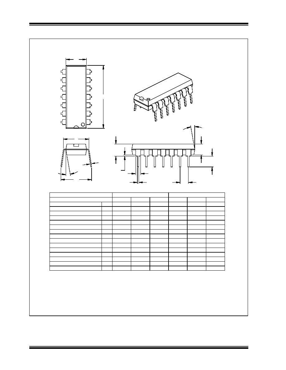
HCS473
DS40035C-page 58
Preliminary
2002 Microchip Technology Inc.
14-Lead Plastic Dual In-line (P) � 300 mil (PDIP)
E1
n
D
1
2
eB
E
c
A
A1
B
B1
L
A2
p
Units
INCHES*
MILLIMETERS
Dimension Limits
MIN
NOM
MAX
MIN
NOM
MAX
Number of Pins
n
14
14
Pitch
p
.100
2.54
Top to Seating Plane
A
.140
.155
.170
3.56
3.94
4.32
Molded Package Thickness
A2
.115
.130
.145
2.92
3.30
3.68
Base to Seating Plane
A1
.015
0.38
Shoulder to Shoulder Width
E
.300
.313
.325
7.62
7.94
8.26
Molded Package Width
E1
.240
.250
.260
6.10
6.35
6.60
Overall Length
D
.740
.750
.760
18.80
19.05
19.30
Tip to Seating Plane
L
.125
.130
.135
3.18
3.30
3.43
Lead Thickness
c
.008
.012
.015
0.20
0.29
0.38
Upper Lead Width
B1
.045
.058
.070
1.14
1.46
1.78
Lower Lead Width
B
.014
.018
.022
0.36
0.46
0.56
Overall Row Spacing
�
eB
.310
.370
.430
7.87
9.40
10.92
Mold Draft Angle Top
5
10
15
5
10
15
5
10
15
5
10
15
Mold Draft Angle Bottom
* Controlling Parameter
Notes:
Dimensions D and E1 do not include mold flash or protrusions. Mold flash or protrusions shall not exceed
.010" (0.254 mm) per side.
JEDEC Equivalent: MS-001
Drawing No. C04-005
� Significant Characteristic
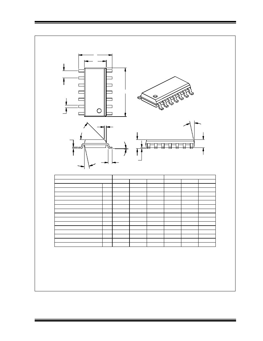
2002 Microchip Technology Inc.
Preliminary
DS40035C-page 59
HCS473
14-Lead Plastic Small Outline (SL) � Narrow, 150 mil (SOIC)
Foot Angle
0
4
8
0
4
8
15
12
0
15
12
0
Mold Draft Angle Bottom
15
12
0
15
12
0
Mold Draft Angle Top
0.51
0.42
0.36
.020
.017
.014
B
Lead Width
0.25
0.23
0.20
.010
.009
.008
c
Lead Thickness
1.27
0.84
0.41
.050
.033
.016
L
Foot Length
0.51
0.38
0.25
.020
.015
.010
h
Chamfer Distance
8.81
8.69
8.56
.347
.342
.337
D
Overall Length
3.99
3.90
3.81
.157
.154
.150
E1
Molded Package Width
6.20
5.99
5.79
.244
.236
.228
E
Overall Width
0.25
0.18
0.10
.010
.007
.004
A1
Standoff�
1.55
1.42
1.32
.061
.056
.052
A2
Molded Package Thickness
1.75
1.55
1.35
.069
.061
.053
A
Overall Height
1.27
.050
p
Pitch
14
14
n
Number of Pins
MAX
NOM
MIN
MAX
NOM
MIN
Dimension Limits
MILLIMETERS
INCHES*
Units
2
1
D
p
n
B
E
E1
h
L
c
45
�
A2
A
A1
* Controlling Parameter
Notes:
Dimensions D and E1 do not include mold flash or protrusions. Mold flash or protrusions shall not exceed
.010" (0.254 mm) per side.
JEDEC Equivalent: MS-012
Drawing No. C04-065
� Significant Characteristic

HCS473
DS40035C-page 60
Preliminary
2002 Microchip Technology Inc.
NOTES:

2002 Microchip Technology Inc.
Preliminary
DS40035C-page 61
HCS473
INDEX
A
AC Characteristics .............................................................. 52
Anti-Collision Off ................................................................. 30
Assembler
MPASM Assembler ..................................................... 43
C
CODE HOPPING COMMAND ('110') ................................. 29
Code Hopping Modulation Format ...................................... 13
Configuration Summary ...................................................... 35
Consecutive Command Considerations.............................. 30
Counter Overflow Bits (OVR1, OVR0) ................................ 18
Cycle Redundancy Check (CRC) ....................................... 18
D
DATA .................................................................................... 6
DC Characteristics .............................................................. 50
Development Support ......................................................... 43
Device Description ................................................................ 5
Device Operation ................................................................ 11
Discrimination Value (DISC) ............................................... 18
E
Electrical Characteristics
Absolute Maximum Ratings ........................................ 49
Encoder Activation .............................................................. 11
Encoder Interface.................................................................. 7
Encoder Mode Options ....................................................... 14
Encoder Operation ................................................................ 1
Encoder Security................................................................... 1
Errata .................................................................................... 2
G
General Description .............................................................. 3
H
HCS473 Hopping Code ........................................................ 4
HCS473 Security .................................................................. 4
HCS473 Transponder Start Sequence ............................... 22
I
ICEPIC In-Circuit Emulator ................................................. 44
IFF Challenge and Response ............................................. 26
Integrating the HCS473 Into A System ............................... 39
Internal RC Oscillator ............................................................ 9
K
KEELOQ Evaluation and Programming Tools .................... 46
Key Terms............................................................................. 3
L
lccom..................................................................................... 7
LED ....................................................................................... 7
LED Operation .................................................................... 17
LF Communication Analog Delays...................................... 30
LF Response Considerations.............................................. 30
Low Voltage Detector............................................................ 9
Low-End System Security Risks ........................................... 4
M
MPLAB C17 and MPLAB C18 C Compilers........................ 43
MPLAB ICD In-Circuit Debugger ........................................ 45
MPLAB ICE High Performance Universal In-Circuit Emulator
with MPLAB IDE ................................................................. 44
MPLAB Integrated Development Environment Software.... 43
MPLINK Object Linker/MPLIB Object Librarian .................. 44
P
Packaging Information ........................................................ 57
Peripherals ........................................................................... 1
PICDEM 1 Low Cost PICmicro Demonstration Board ........ 45
PICDEM 17 Demonstration Board...................................... 46
PICDEM 2 Low Cost PIC16CXX Demonstration Board ..... 45
PICDEM 3 Low Cost PIC16CXXX Demonstration Board ... 46
PICSTART Plus Entry Level Development Programmer.... 45
Present Transport Code ..................................................... 25
PRO MATE II Universal Device Programmer ..................... 45
Product Identification System ............................................. 64
Programming Specification................................................. 37
R
Read Sequence .................................................................. 27
Receive Stability - Calculating Communiction .................... 32
Request Hopping Code Command..................................... 29
RFEN During LF Communication ....................................... 33
S
S0 ......................................................................................... 6
s3 .......................................................................................... 6
Select Transponder ............................................................ 24
Software Simulator (MPLAB SIM) ...................................... 44
T
Transmitted Code Word...................................................... 11
Transponder Characteristics............................................... 51
Transponder Commands .................................................... 23
Transponder Communication ............................................. 21
Transponder Interface .......................................................... 8
Transponder Mode ............................................................. 18
Transponder Operation......................................................... 1
Transponder Options .......................................................... 19
Transponder Security ........................................................... 1
Typical Applications .............................................................. 1
W
Wake-Up Logic ..................................................................... 7
WWW, On-Line Support ....................................................... 2

HCS473
DS40035C-page 62
Preliminary
2002 Microchip Technology Inc.
SYSTEMS INFORMATION AND
UPGRADE HOT LINE
The Systems Information and Upgrade Line provides
system users a listing of the latest versions of all of
Microchip's development systems software products.
Plus, this line provides information on how customers
can receive the most current upgrade kits.The Hot Line
Numbers are:
1-800-755-2345 for U.S. and most of Canada, and
1-480-792-7302 for the rest of the world.
ON-LINE SUPPORT
Microchip provides on-line support on the Microchip
World Wide Web site.
The web site is used by Microchip as a means to make
files and information easily available to customers. To
view the site, the user must have access to the Internet
and a web browser, such as Netscape
�
or Microsoft
�
Internet Explorer. Files are also available for FTP
download from our FTP site.
Connecting to the Microchip Internet Web Site
The Microchip web site is available at the following
URL:
www.microchip.com
The file transfer site is available by using an FTP ser-
vice to connect to:
ftp://ftp.microchip.com
The web site and file transfer site provide a variety of
services. Users may download files for the latest
Development Tools, Data Sheets, Application Notes,
User's Guides, Articles and Sample Programs. A vari-
ety of Microchip specific business information is also
available, including listings of Microchip sales offices,
distributors and factory representatives. Other data
available for consideration is:
� Latest Microchip Press Releases
� Technical Support Section with Frequently Asked
Questions
� Design Tips
� Device Errata
� Job Postings
� Microchip Consultant Program Member Listing
� Links to other useful web sites related to
Microchip Products
� Conferences for products, Development Systems,
technical information and more
� Listing of seminars and events
092002

2002 Microchip Technology Inc.
Preliminary
DS40035C-page 63
HCS473
READER RESPONSE
It is our intention to provide you with the best documentation possible to ensure successful use of your Microchip prod-
uct. If you wish to provide your comments on organization, clarity, subject matter, and ways in which our documentation
can better serve you, please FAX your comments to the Technical Publications Manager at (480) 792-4150.
Please list the following information, and use this outline to provide us with your comments about this document.
1.
What are the best features of this document?
2.
How does this document meet your hardware and software development needs?
3.
Do you find the organization of this document easy to follow? If not, why?
4.
What additions to the document do you think would enhance the structure and subject?
5.
What deletions from the document could be made without affecting the overall usefulness?
6.
Is there any incorrect or misleading information (what and where)?
7.
How would you improve this document?
To:
Technical Publications Manager
RE:
Reader Response
Total Pages Sent ________
From: Name
Company
Address
City / State / ZIP / Country
Telephone: (_______) _________ - _________
Application (optional):
Would you like a reply? Y N
Device:
Literature Number:
Questions:
FAX: (______) _________ - _________
DS40035C
HCS473

HCS473
DS40035C-page64
Preliminary
2002 Microchip Technology Inc.
PRODUCT IDENTIFICATION SYSTEM
To order or obtain information, e.g., on pricing or delivery, refer to the factory or the listed sales office.
* JW Devices are UV erasable and can be programmed to any device configuration. JW Devices meet the electrical requirement of
each oscillator type.
Sales and Support
Data Sheets
Products supported by a preliminary Data Sheet may have an errata sheet describing minor operational differences and recom-
mended workarounds. To determine if an errata sheet exists for a particular device, please contact one of the following:
1.
Your local Microchip sales office
2.
The Microchip Corporate Literature Center U.S. FAX: (480) 792-7277
3.
The Microchip Worldwide Site (www.microchip.com)
Please specify which device, revision of silicon and Data Sheet (include Literature #) you are using.
New Customer Notification System
Register on our web site (www.microchip.com/cn) to receive the most current information on our products.
PART NO.
X
/XX
XXX
Pattern
Package
Temperature
Range
Device
Device
HCS473
Temperature Range
-
=
0
�C to +70�C
I
=
-20
�C to +85�C
Package
P
=
PDIP
SL
=
SOIC
Pattern
QTP, SQTP, ROM Code (factory specified) or
Special Requirements . Blank for OTP and
Windowed devices.
Examples:
a)
To be supplied.

2002 Microchip Technology Inc.
Preliminary
DS40035C-page 65
HCS473
NOTES:

DS40035C-page 66
Preliminary
2002 Microchip Technology Inc.
AMERICAS
Corporate Office
2355 West Chandler Blvd.
Chandler, AZ 85224-6199
Tel: 480-792-7200 Fax: 480-792-7277
Technical Support: 480-792-7627
Web Address: http://www.microchip.com
Rocky Mountain
2355 West Chandler Blvd.
Chandler, AZ 85224-6199
Tel: 480-792-7966 Fax: 480-792-4338
Atlanta
500 Sugar Mill Road, Suite 200B
Atlanta, GA 30350
Tel: 770-640-0034 Fax: 770-640-0307
Boston
2 Lan Drive, Suite 120
Westford, MA 01886
Tel: 978-692-3848 Fax: 978-692-3821
Chicago
333 Pierce Road, Suite 180
Itasca, IL 60143
Tel: 630-285-0071 Fax: 630-285-0075
Dallas
4570 Westgrove Drive, Suite 160
Addison, TX 75001
Tel: 972-818-7423 Fax: 972-818-2924
Detroit
Tri-Atria Office Building
32255 Northwestern Highway, Suite 190
Farmington Hills, MI 48334
Tel: 248-538-2250 Fax: 248-538-2260
Kokomo
2767 S. Albright Road
Kokomo, Indiana 46902
Tel: 765-864-8360 Fax: 765-864-8387
Los Angeles
18201 Von Karman, Suite 1090
Irvine, CA 92612
Tel: 949-263-1888 Fax: 949-263-1338
San Jose
Microchip Technology Inc.
2107 North First Street, Suite 590
San Jose, CA 95131
Tel: 408-436-7950 Fax: 408-436-7955
Toronto
6285 Northam Drive, Suite 108
Mississauga, Ontario L4V 1X5, Canada
Tel: 905-673-0699 Fax: 905-673-6509
ASIA/PACIFIC
Australia
Microchip Technology Australia Pty Ltd
Suite 22, 41 Rawson Street
Epping 2121, NSW
Australia
Tel: 61-2-9868-6733 Fax: 61-2-9868-6755
China - Beijing
Microchip Technology Consulting (Shanghai)
Co., Ltd., Beijing Liaison Office
Unit 915
Bei Hai Wan Tai Bldg.
No. 6 Chaoyangmen Beidajie
Beijing, 100027, No. China
Tel: 86-10-85282100 Fax: 86-10-85282104
China - Chengdu
Microchip Technology Consulting (Shanghai)
Co., Ltd., Chengdu Liaison Office
Rm. 2401, 24th Floor,
Ming Xing Financial Tower
No. 88 TIDU Street
Chengdu 610016, China
Tel: 86-28-86766200 Fax: 86-28-86766599
China - Fuzhou
Microchip Technology Consulting (Shanghai)
Co., Ltd., Fuzhou Liaison Office
Unit 28F, World Trade Plaza
No. 71 Wusi Road
Fuzhou 350001, China
Tel: 86-591-7503506 Fax: 86-591-7503521
China - Shanghai
Microchip Technology Consulting (Shanghai)
Co., Ltd.
Room 701, Bldg. B
Far East International Plaza
No. 317 Xian Xia Road
Shanghai, 200051
Tel: 86-21-6275-5700 Fax: 86-21-6275-5060
China - Shenzhen
Microchip Technology Consulting (Shanghai)
Co., Ltd., Shenzhen Liaison Office
Rm. 1315, 13/F, Shenzhen Kerry Centre,
Renminnan Lu
Shenzhen 518001, China
Tel: 86-755-82350361 Fax: 86-755-82366086
China - Hong Kong SAR
Microchip Technology Hongkong Ltd.
Unit 901-6, Tower 2, Metroplaza
223 Hing Fong Road
Kwai Fong, N.T., Hong Kong
Tel: 852-2401-1200 Fax: 852-2401-3431
India
Microchip Technology Inc.
India Liaison Office
Divyasree Chambers
1 Floor, Wing A (A3/A4)
No. 11, O'Shaugnessey Road
Bangalore, 560 025, India
Tel: 91-80-2290061 Fax: 91-80-2290062
Japan
Microchip Technology Japan K.K.
Benex S-1 6F
3-18-20, Shinyokohama
Kohoku-Ku, Yokohama-shi
Kanagawa, 222-0033, Japan
Tel: 81-45-471- 6166 Fax: 81-45-471-6122
Korea
Microchip Technology Korea
168-1, Youngbo Bldg. 3 Floor
Samsung-Dong, Kangnam-Ku
Seoul, Korea 135-882
Tel: 82-2-554-7200 Fax: 82-2-558-5934
Singapore
Microchip Technology Singapore Pte Ltd.
200 Middle Road
#07-02 Prime Centre
Singapore, 188980
Tel: 65-6334-8870 Fax: 65-6334-8850
Taiwan
Microchip Technology (Barbados) Inc.,
Taiwan Branch
11F-3, No. 207
Tung Hua North Road
Taipei, 105, Taiwan
Tel: 886-2-2717-7175 Fax: 886-2-2545-0139
EUROPE
Austria
Microchip Technology Austria GmbH
Durisolstrasse 2
A-4600 Wels
Austria
Tel: 43-7242-2244-399
Fax: 43-7242-2244-393
Denmark
Microchip Technology Nordic ApS
Regus Business Centre
Lautrup hoj 1-3
Ballerup DK-2750 Denmark
Tel: 45 4420 9895 Fax: 45 4420 9910
France
Microchip Technology SARL
Parc d'Activite du Moulin de Massy
43 Rue du Saule Trapu
Batiment A - ler Etage
91300 Massy, France
Tel: 33-1-69-53-63-20 Fax: 33-1-69-30-90-79
Germany
Microchip Technology GmbH
Steinheilstrasse 10
D-85737 Ismaning, Germany
Tel: 49-89-627-144 0 Fax: 49-89-627-144-44
Italy
Microchip Technology SRL
Centro Direzionale Colleoni
Palazzo Taurus 1 V. Le Colleoni 1
20041 Agrate Brianza
Milan, Italy
Tel: 39-039-65791-1 Fax: 39-039-6899883
United Kingdom
Microchip Ltd.
505 Eskdale Road
Winnersh Triangle
Wokingham
Berkshire, England RG41 5TU
Tel: 44 118 921 5869 Fax: 44-118 921-5820
10/18/02
W
ORLDWIDE
S
ALES
AND
S
ERVICE