©
2002 Microchip Technology Inc.
DS40153C-page 1
HCS500
FEATURES
Security
∑ Encrypted storage of manufacturer's code
∑ Encrypted storage of crypt keys
∑ Up to seven transmitters can be learned
∑ K
EE
L
OQ
code hopping technology
∑ Normal and Secure learning mechanisms
Operating
∑ 3.0V--5.5V operation
∑ Internal oscillator
∑ Auto bit rate detection
Other
∑ Stand-alone decoder chipset
∑ External EEPROM for transmitter storage
∑ Synchronous serial interface
∑ 1 Kbit user EEPROM
∑ 8-pin DIP/SOIC package
Typical Applications
∑ Automotive remote entry systems
∑ Automotive alarm systems
∑ Automotive immobilizers
∑ Gate and garage openers
∑ Electronic door locks
∑ Identity tokens
∑ Burglar alarm systems
Compatible Encoders
All K
EE
L
OQ
encoders and transponders configured for
the following setting:
∑ PWM modulation format (1/3-2/3)
∑ T
E
in the range from 100us to 400us
∑ 10 x T
E
Header
∑ 28-bit Serial Number
∑ 16-bit Synchronization counter
∑ Discrimination bits equal to Serial Number 8 LSbs
∑ 66- to 69-bit length code word.
DESCRIPTION
The Microchip Technology Inc. HCS500 is a code hop-
ping decoder designed for secure Remote Keyless
Entry (RKE) systems. The HCS500 utilizes the pat-
ented K
EE
L
OQ
Æ
code hopping system and high security
learning mechanisms to make this a canned solution
when used with the HCS encoders to implement a uni-
directional remote and access control systems. The
HCS500 can be used as a stand-alone decoder or in
conjunction with a microcontroller.
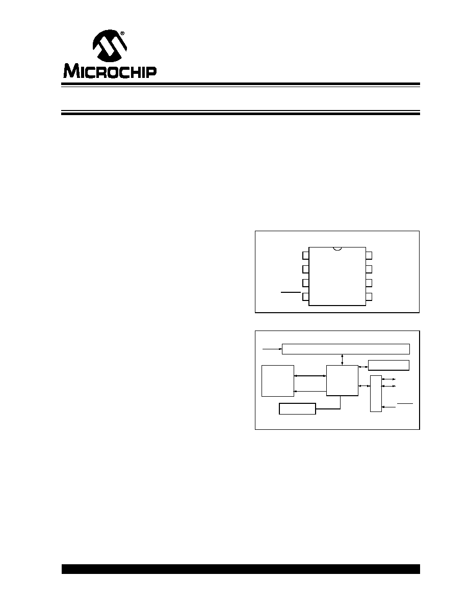
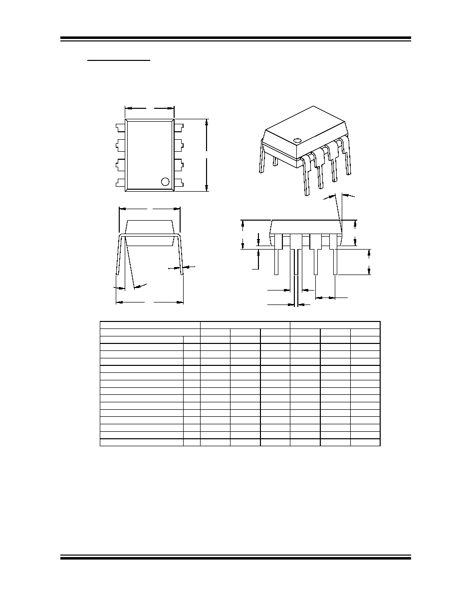
PACKAGE TYPE
BLOCK DIAGRAM
The manufacturer's code, crypt keys, and synchroniza-
tion information are stored in encrypted form in external
EEPROM. The HCS500 uses the S_DAT and S_CLK
inputs to communicate with a host controller device.
The HCS500 operates over a wide voltage range of
3.0 volts to 5.5 volts. The decoder employs automatic
bit-rate detection, which allows it to compensate for
wide variations in transmitter data rate. The decoder
contains sophisticated error checking algorithms to
ensure only valid codes are accepted.
HCS5
0
0
PDIP, SOIC
1
2
3
4
V
DD
EE_CLK
EE_DAT
MCLR
8
7
6
5
V
SS
RFIN
S_CLK
S_DAT
Reception Register
External
CONTROL
DECRYPTOR
RFIN
OSCILLATOR
S_DAT
S_CLK
MCLR
EEPROM
EE_DAT
EE_CLK
K
EE
L
OQ
Æ
Code Hopping Decoder

HCS500
DS40153C-page 2
©
2002 Microchip Technology Inc.
1.0
SYSTEM OVERVIEW
Key Terms
The following is a list of key terms used throughout this
data sheet. For additional information on K
EE
L
OQ
and
Code Hopping, refer to Technical Brief 3 (TB003).
∑ RKE - Remote Keyless Entry
∑ Button Status - Indicates what button input(s)
activated the transmission. Encompasses the 4
button status bits S3, S2, S1 and S0 (Figure 7-2).
∑ Code Hopping - A method by which a code,
viewed externally to the system, appears to
change unpredictably each time it is transmitted.
∑ Code word - A block of data that is repeatedly
transmitted upon button activation (Figure 7-1).
∑ Transmission - A data stream consisting of
repeating code words (Figure 7-1).
∑ Crypt key - A unique and secret 64-bit number
used to encrypt and decrypt data. In a symmetri-
cal block cipher such as the K
EE
L
OQ
algorithm,
the encryption and decryption keys are equal and
will therefore be referred to generally as the crypt
key.
∑ Encoder - A device that generates and encodes
data.
∑ Encryption Algorithm - A recipe whereby data is
scrambled using a crypt key. The data can only be
interpreted by the respective decryption algorithm
using the same crypt key.
∑ Decoder - A device that decodes data received
from an encoder.
∑ Decryption algorithm - A recipe whereby data
scrambled by an encryption algorithm can be
unscrambled using the same crypt key.
∑ Learn ≠ Learning involves the receiver calculating
the transmitter's appropriate crypt key, decrypting
the received hopping code and storing the serial
number, synchronization counter value and crypt
key in EEPROM. The K
EE
L
OQ
product family facil-
itates several learning strategies to be imple-
mented on the decoder. The following are
examples of what can be done.
- Simple Learning
The receiver uses a fixed crypt key, common
to all components of all systems by the same
manufacturer, to decrypt the received code
word's encrypted portion.
- Normal Learning
The receiver uses information transmitted
during normal operation to derive the crypt
key and decrypt the received code word's
encrypted portion.
- Secure Learn
The transmitter is activated through a special
button combination to transmit a stored 60-bit
seed value used to generate the transmitter's
crypt key. The receiver uses this seed value
to derive the same crypt key and decrypt the
received code word's encrypted portion.
∑ Manufacturer's code ≠ A unique and secret 64-
bit number used to generate unique encoder crypt
keys. Each encoder is programmed with a crypt
key that is a function of the manufacturer's code.
Each decoder is programmed with the manufac-
turer code itself.
1.1
HCS Encoder Overview
The HCS encoders have a small EEPROM array which
must be loaded with several parameters before use.
The most important of these values are:
∑ A crypt key that is generated at the time of pro-
duction
∑ A 16-bit synchronization counter value
∑ A 28-bit serial number which is meant to be
unique for every encoder
The manufacturer programs the serial number for each
encoder at the time of production, while the `Key Gen-
eration Algorithm' generates the crypt key (Figure 1-1).
Inputs to the key generation algorithm typically consist
of the encoder's serial number and a 64-bit manufac-
turer's code, which the manufacturer creates.
Note:
The manufacturer code is a pivotal part of
the system's overall security. Conse-
quently, all possible precautions must be
taken and maintained for this code.
©
2002 Microchip Technology Inc.
DS40153C-page 3
HCS500
FIGURE 1-1:
CREATION AND STORAGE OF CRYPT KEY DURING PRODUCTION
The 16-bit synchronization counter is the basis behind
the transmitted code word changing for each transmis-
sion; it increments each time a button is pressed. Due
to the code hopping algorithm's complexity, each incre-
ment of the synchronization value results in greater
than 50% of the bits changing in the transmitted code
word.
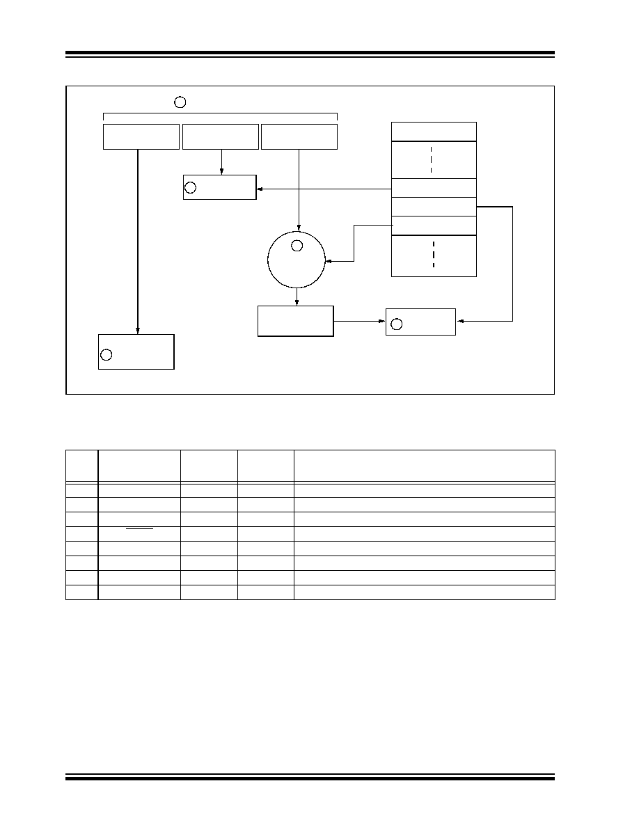
Figure 1-2 shows how the key values in EEPROM are
used in the encoder. Once the encoder detects a button
press, it reads the button inputs and updates the syn-
chronization counter. The synchronization counter and
crypt key are input to the encryption algorithm and the
output is 32 bits of encrypted information. This data will
change with every button press, its value appearing
externally to `randomly hop around', hence it is referred
to as the hopping portion of the code word. The 32-bit
hopping code is combined with the button information
and serial number to form the code word transmitted to
the receiver. The code word format is explained in
greater detail in Section 7.2.
A receiver may use any type of controller as a decoder,
but it is typically a microcontroller with compatible firm-
ware that allows the decoder to operate in conjunction
with an HCS500 based transmitter. Section 3.0
provides detail on integrating the HCS500 into a sys-
tem.
A transmitter must first be `learned' by the receiver
before its use is allowed in the system. Learning
includes calculating the transmitter's appropriate crypt
key, decrypting the received hopping code and storing
the serial number, synchronization counter value and
crypt key in EEPROM.
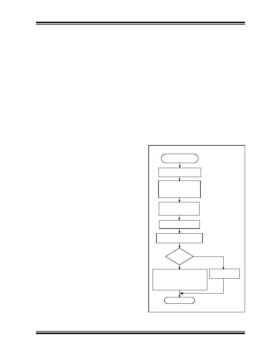
In normal operation, each received message of valid
format is evaluated. The serial number is used to deter-
mine if it is from a learned transmitter. If from a learned
transmitter, the message is decrypted and the synchro-
nization counter is verified. Finally, the button status is
checked to see what operation is requested. Figure 1-3
shows the relationship between some of the values
stored by the receiver and the values received from
the transmitter.
FIGURE 1-2:
BUILDING THE TRANSMITTED CODE WORD (ENCODER)
Transmitter
Manufacturer's
Serial Number
Code
Crypt
Key
Key
Generation
Algorithm
Serial Number
Crypt Key
Sync Counter
.
.
.
HCS500
Production
Programmer
EEPROM Array
Button Press
Information
EEPROM Array
32 Bits
Encrypted Data
Serial Number
Transmitted Information
Crypt Key
Sync Counter
Serial Number
K
EE
L
OQ
Encryption
Algorithm
HCS500
DS40153C-page 4
©
2002 Microchip Technology Inc.
FIGURE 1-3:
BASIC OPERATION OF RECEIVER (DECODER)
Note: Circled numbers indicate the order of execution.
2.0
PIN ASSIGNMENT
Button Press
Information
EEPROM Array
Manufacturer Code
32 Bits of
Encrypted Data
Serial Number
Received Information
Decrypted
Synchronization
Counter
Check for
Match
Sync Counter
Serial Number
K
EE
L
OQ
Decryption
Algorithm
1
3
4
Check for
Match
2
Perform Function
Indicated by
button press
5
Crypt Key
PIN
Decoder
Function
I/O
(1)
Buffer
Type
(1)
Description
1
V
DD
P
--
Power Connection
2
EE_CLK
O
TTL
Clock to I
2
C
TM
EEPROM
3
EE_DAT
I/O
TTL
Data to I
2
C EEPROM
4
MCLR
I
ST
Master clear input
5
S_DAT
I/O
TTL
Synchronous data from controller
6
S_CLK
I
TTL
Synchronous clock from controller
7
RFIN
I
TTL
RF input from receiver
8
GND
P
--
Ground connection
Note: P = power, I = in, O = out, and ST = Schmitt Trigger input.
©
2002 Microchip Technology Inc.
DS40153C-page 5
HCS500
3.0
DECODER OPERATION
3.1
Learning a Transmitter to a
Receiver (Normal or Secure Learn)
Before the transmitter and receiver can work together,
the receiver must first `learn' and store the following
information from the transmitter in EEPROM:
∑ A check value of the serial number
∑ The crypt key
∑ The current synchronization counter value
The decoder must also store the manufacturer's code
(Section 1.1) in protected memory. This code will
typically be the same for all of the decoders in a sys-
tem.
The HCS500 has seven memory slots, and, conse-
quently, can store up to seven transmitters. During the
learn procedure, the decoder searches for an empty
memory slot for storing the transmitter's information.
When all of the memory slots are full, the decoder will
overwrite the last transmitter's information. To erase all
of the memory slots at once, use the ERASE_ALL com-
mand (C3H).
3.2
LEARNING PROCEDURE
Learning is initiated by sending the ACTIVATE_LEARN
(D2H) command to the decoder. The decoder acknowl-
edges reception of the command by pulling the data
line high.
For the HCS500 decoder to learn a new transmitter, the
following sequence is required:
1.
Activate the transmitter once.
2.
Activate the transmitter a second time. (In
Secure Learning mode, the seed transmission
must be transmitted during the second stage of
learn by activating the appropriate buttons on
the transmitter.)
The HCS500 will transmit a learn-status string,
indicating that the learn was successful.
3.
The decoder has now learned the transmitter.
4.
Repeat steps 1-3 to learn up to seven
transmitters
Note 1: Learning will be terminated if two
nonsequential codes were received or if
two acceptable codes were not decoded
within 30 seconds.
2: If more than seven transmitters are
learned, the new transmitter will replace
the last transmitter learned. It is, therefore,
not possible to erase lost transmitters by
repeatedly learning new transmitters. To
remove lost or stolen transmitters,
ERASE_ALL transmitters and relearn all
available transmitters.
3: Learning a transmitter with a crypt key that
is identical to a transmitter already in mem-
ory replaces the existing transmitter. In
practice, this means that all transmitters
should have unique crypt keys. Learning a
previously learned transmitter does not use
any additional memory slots.
The following checks are performed by the decoder to
determine if the transmission is valid during learn:
∑ The first code word is checked for bit integrity.
∑ The second code word is checked for bit integrity.
∑ The crypt key is generated according to the
selected algorithm.
∑ The hopping code is decrypted.
∑ The discrimination value is checked.
∑ If all the checks pass, the key, serial number
check value, and synchronization counter values
are stored in EEPROM memory.
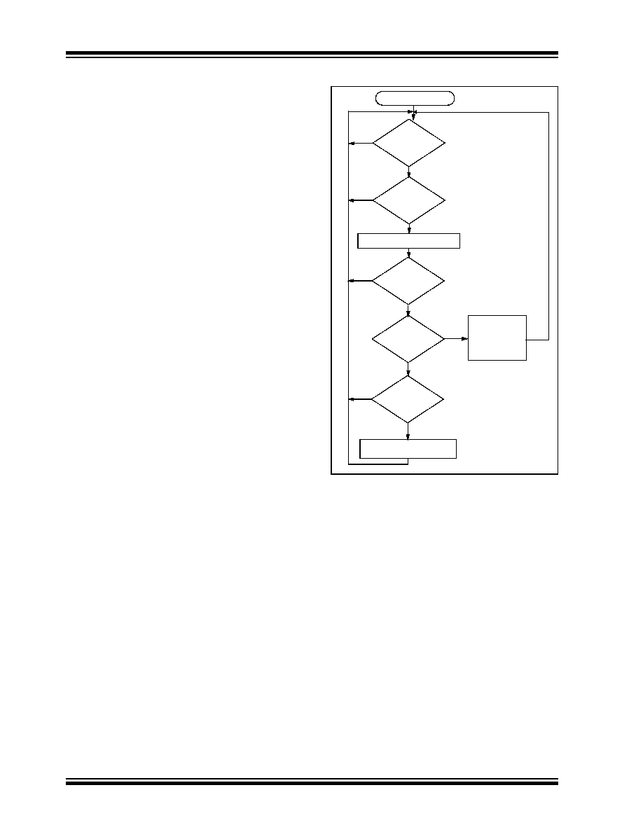
Figure 3-1 shows a flow chart of the learn sequence.
FIGURE 3-1:
LEARN SEQUENCE
Enter Learn
Mode
Wait for Reception
of Second
Compare Discrimination
Value with Serial Number
Use Generated Key
to Decrypt
Equal?
Sync. counter value
crypt key
Exit
Learn successful. Store:
Learn
Unsuccessful
No
Yes
Wait for Reception
of a Valid Code
Non-Repeated
Valid Code
Generate Key
from Serial Number/
Seed Value
Serial number check value
HCS500
DS40153C-page 6
©
2002 Microchip Technology Inc.
3.3
Validation of Codes
The decoder waits for a transmission and checks the
serial number to determine if it is a learned transmitter.
If it is, it takes the code hopping portion of the transmis-
sion and decrypts it, using the crypt key. It uses the dis-
crimination value to determine if the decryption was
valid. If everything up to this point is valid, the
synchronization counter value is evaluated.
3.4
Validation Steps
Validation consists of the following steps:
1.
Search EEPROM to find the Serial Number
Check Value Match
2.
Decrypt the Hopping Code
3.
Compare the 10 bits of the discrimination value
with the lower 10 bits of serial number
4.
Check if the synchronization counter value falls
within the first synchronization window.
5.
Check if the synchronization counter value falls
within the second synchronization window.
6.
If a valid transmission is found, update the
synchronization counter, else use the next
transmitter block, and repeat the tests.
FIGURE 3-2:
DECODER OPERATION
Transmission
Received?
Does
Ser # Check Val
Match?
Decrypt Transmission
Is
decryption
valid?
Is
counter within
16?
Is
counter within
16K?
Update
Counter
Execute
Command
Save Counter
in Temp Location
Start
No
No
No
No
Yes
Yes
Yes
Yes
Yes
No
and
©
2002 Microchip Technology Inc.
DS40153C-page 7
HCS500
3.5
Synchronization with Decoder
(Evaluating the Counter)
The K
EE
L
OQ
technology patent scope includes a
sophisticated synchronization technique that does not
require the calculation and storage of future codes. The
technique securely blocks invalid transmissions while
providing transparent resynchronization to transmitters
inadvertently activated away from the receiver.
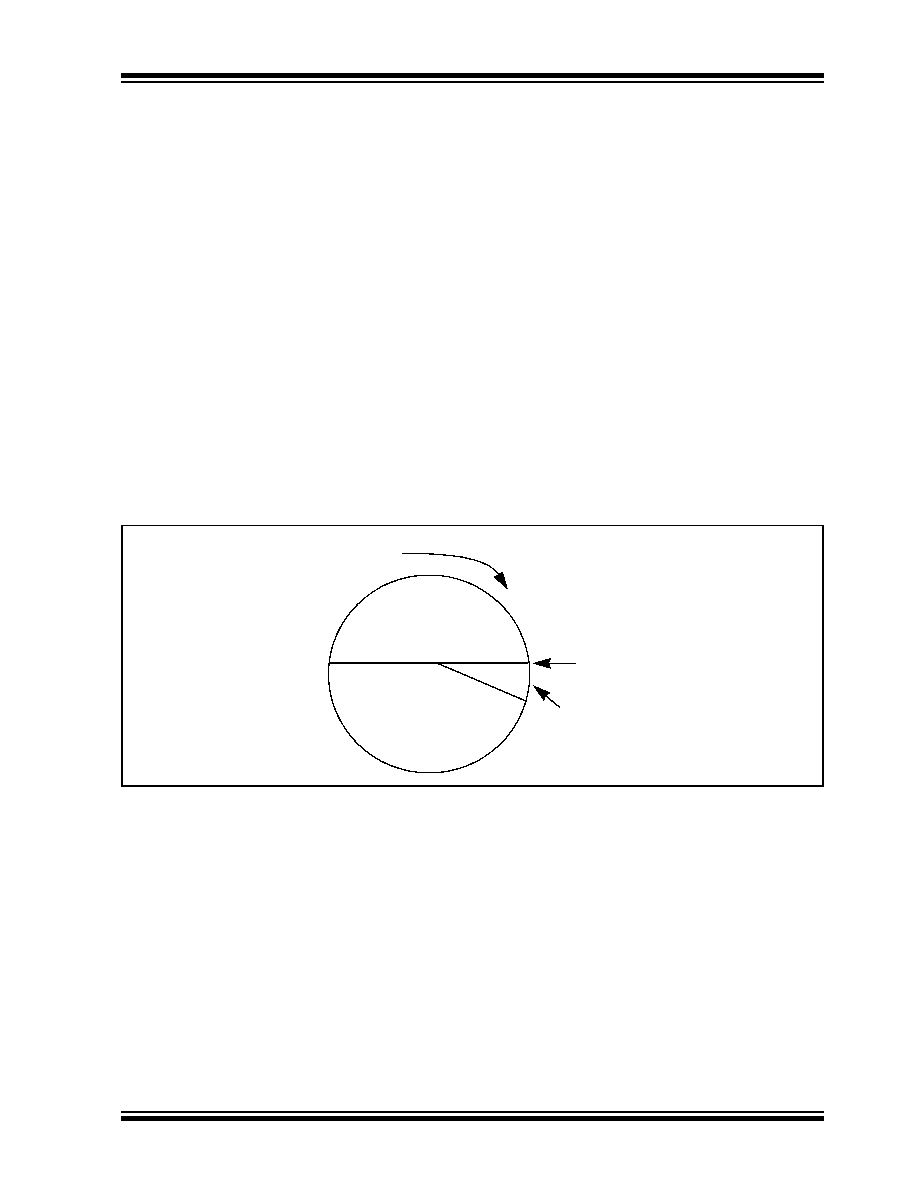
Figure 3-3 shows a 3-partition, rotating synchronization
window. The size of each window is optional but the
technique is fundamental. Each time a transmission is
authenticated, the intended function is executed and
the transmission's synchronization counter value is
stored in EEPROM. From the currently stored counter
value there is an initial "Single Operation" forward win-
dow of 16 codes. If the difference between a received
synchronization counter and the last stored counter is
within 16, the intended function will be executed on the
single button press and the new synchronization
counter will be stored. Storing the new synchronization
counter value effectively rotates the entire synchroniza-
tion window.
A "Double Operation" (resynchronization) window fur-
ther exists from the Single Operation window up to 32K
codes forward of the currently stored counter value. It
is referred to as "Double Operation" because a trans-
mission with synchronization counter value in this win-
dow will require an additional, sequential counter
transmission prior to executing the intended function.
Upon receiving the sequential transmission the
decoder executes the intended function and stores the
synchronization counter value. This resynchronization
occurs transparently to the user as it is human nature
to press the button a second time if the first was unsuc-
cessful.
The third window is a "Blocked Window" ranging from
the double operation window to the currently stored
synchronization counter value. Any transmission with
synchronization counter value within this window will
be ignored. This window excludes previously used,
perhaps code-grabbed transmissions from accessing
the system.
FIGURE 3-3:
SYNCHRONIZATION WINDOW
Blocked
Entire Window
rotates to eliminate
use of previously
used codes
Single Operation
Window
Window
(32K Codes)
(16 Codes)
Double Operation
(resynchronization)
Window
(32K Codes)
Stored
Synchronization
Counter Value
HCS500
DS40153C-page 8
©
2002 Microchip Technology Inc.
4.0
INTERFACING TO A
MICROCONTROLLER
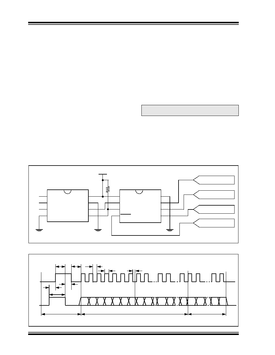
The HCS500 interfaces to a microcontroller via a syn-
chronous serial interface. A clock and data line are
used to communicate with the HCS500. The microcon-
troller controls the clock line. There are two groups of
data transfer messages. The first is from the decoder
whenever the decoder receives a valid transmission.
The decoder signals reception of a valid code by taking
the data line high (maximum of 500 ms) The microcon-
troller then services the request by clocking out a data
string from the decoder. The data string contains the
function code, the status bit, and block indicators. The
second is from the controlling microcontroller to the
decoder in the form of a defined command set.
Figure 4-1 shows the HCS500 decoder and the I/O
interface lines necessary to interface to a microcontrol-
ler.
4.1
Valid Transmission Message
The decoder informs the microcontroller of a valid
transmission by taking the data line high for up to
500 ms. The controlling microcontroller must acknowl-
edge by taking the clock line high. The decoder then
takes the data line low. The microcontroller can then
begin clocking a data stream out of the HCS500. The
data stream consists of:
∑ START bit `0'.
∑ 2 status bits [REPEAT, VLOW].
∑ 4-bit function code [S3 S2 S1 S0].
∑ STOP bit `1'.
∑ 4 bits indicating which block was used
[TX3...TX0].
∑ 4 bits indicating the number of transmitters
learned into the decoder [CNT3...CNT0].
∑ 64 bits of the received transmission with the hop-
ping code decrypted.
The decoder will terminate the transmission of the data
stream at any point where the clock is kept low for
longer than 1 ms. Therefore, the microcontroller can
only clock out the required bits. A maximum of 80 bits
can be clocked out of the decoder.
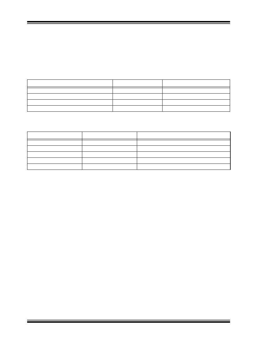
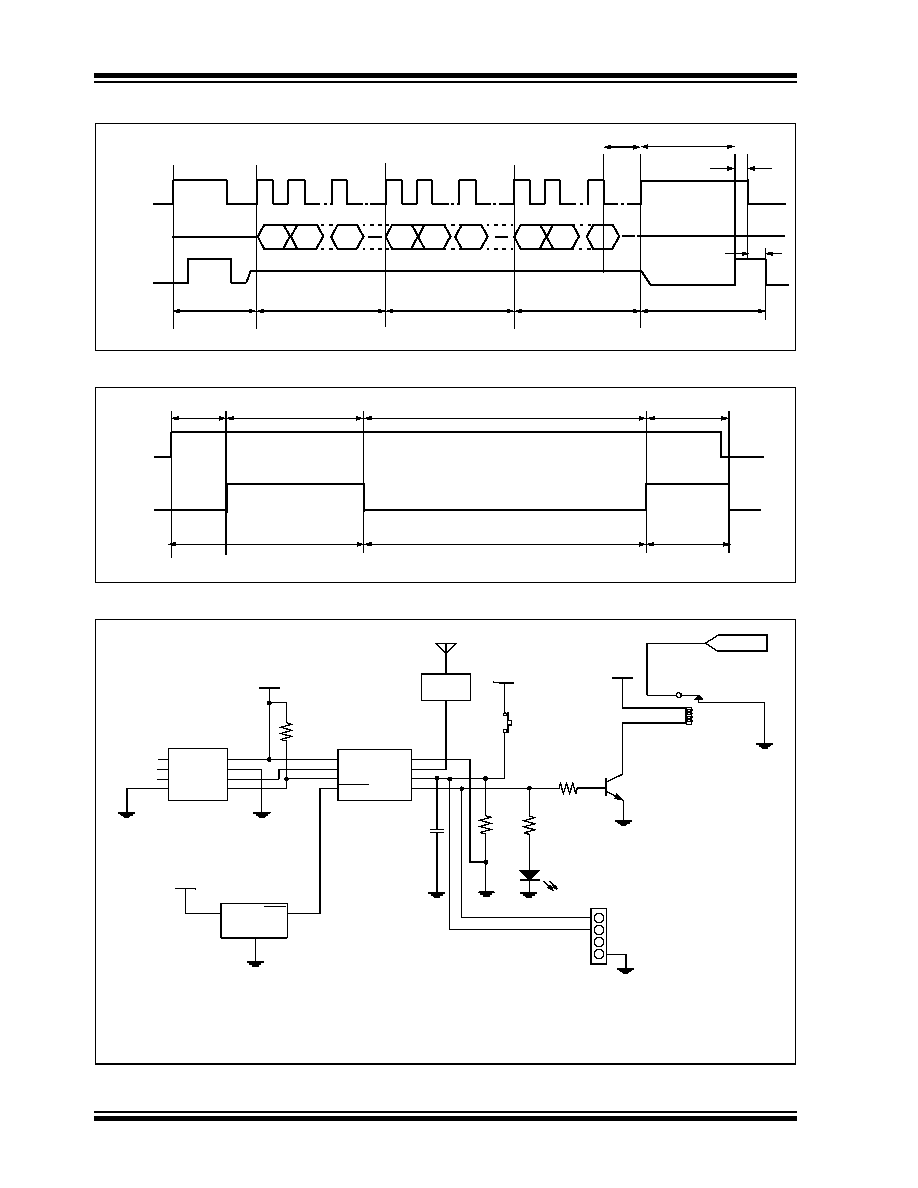
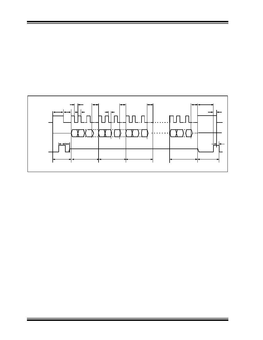
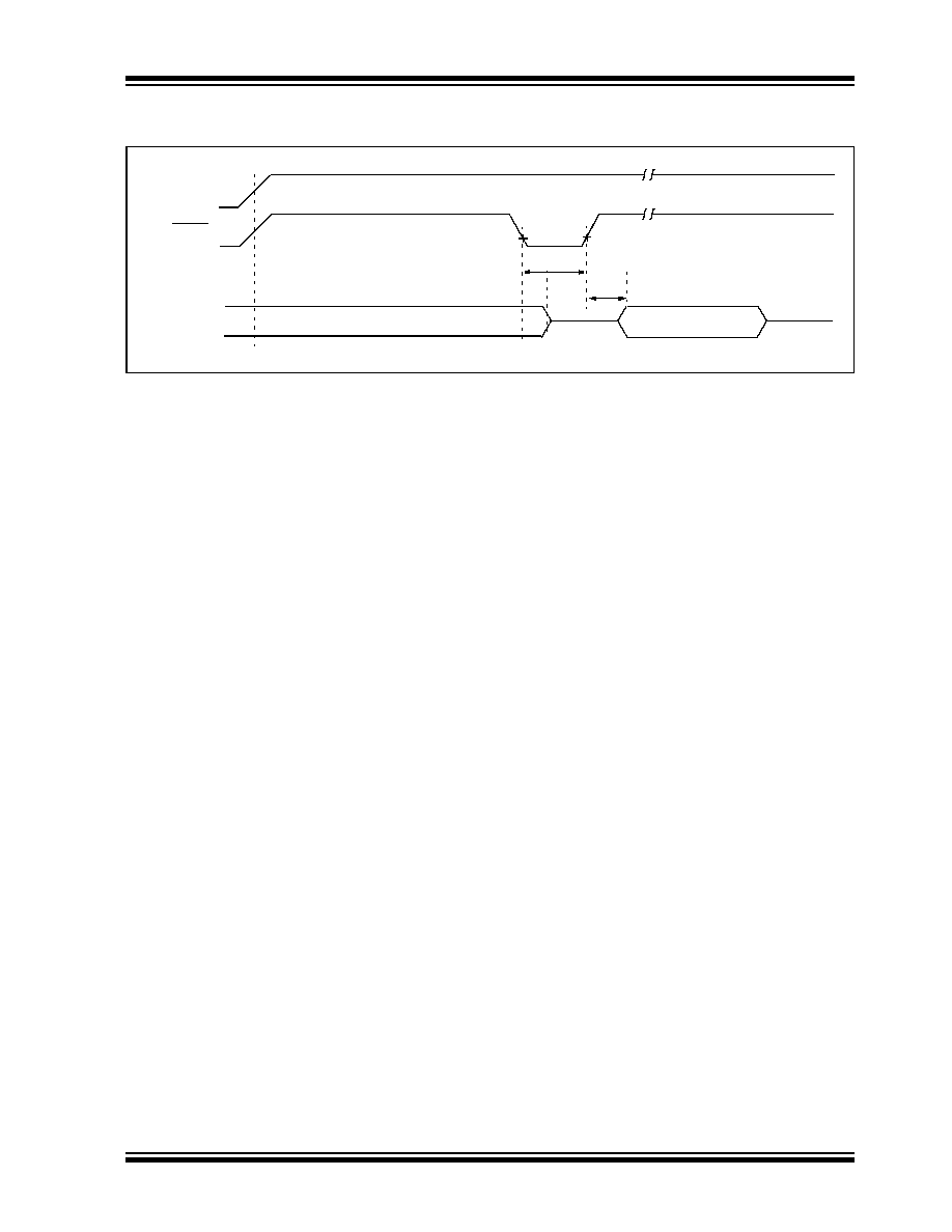
FIGURE 4-1:
HCS500 DECODER AND I/O INTERFACE LINES
FIGURE 4-2:
DECODER VALID TRANSMISSION MESSAGE
Note:
Data is always clocked in/out Least
Significant Bit (LSB) first.
A0
A1
A2
Vss
24LC02
Vcc
WP
SCL
SD
1
2
3
4
8
7
6
5
V
DD
EE_CLK
EE_DAT
MCLR
Vss
RFIN
S_CLK
S_DAT
1
2
3
4
8
7
6
5
V
DD
RF RECEIVER
SYNC CLOCK
SYNC DATA
MICRO RESET
HCS500
1K
Decoder Signal Valid
T
CLKH
T
DS
A
B
Cii
T
PP
3
T
DHI
T
CLA
Received String
Ci
S_DAT
TX0
TX3
RX63
REPT V
LOW
S0
S1
S2
S3
CNT0
CNT3
0
RX0
RX1
RX62
1
S_CLK
Information
T
PP
1
T
CLKH
T
CLKL
Transmission
©
2002 Microchip Technology Inc.
DS40153C-page 9
HCS500
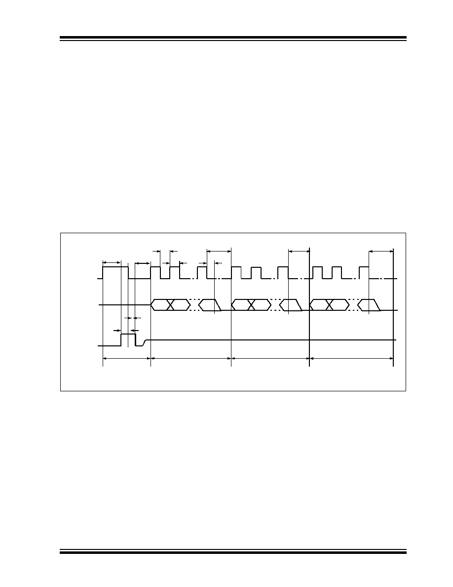
4.2
Command Mode
4.2.1
MICROCONTROLLER COMMAND
MODE ACTIVATION
The microcontroller command consists of four parts.
The first part activates the Command mode, the sec-
ond part is the actual command, the third is the address
accessed, and the last part is the data. The microcon-
troller starts the command by taking the clock line high
for up to 500 ms. The decoder acknowledges the start-
up sequence by taking the data line high. The micro-
controller takes the clock line low, after which the
decoder will take the data line low, tri-state the data line
and wait for the command to be clock in. The data must
be set up on the rising edge and will be sampled on the
falling edge of the clock line.
4.2.2
COLLISION DETECTION
The HCS500 uses collision detection to prevent
clashes between the decoder and microcontroller.
Whenever the decoder receives a valid transmission
the following sequence is followed:
∑ The decoder first checks to see if the clock line is
high. If the clock line is high, the valid transmis-
sion notification is aborted, and the microcontrol-
ler Command mode request is serviced.
∑ The decoder takes the data line high and checks
that the clock line doesn't go high within 50
µ
s. If
the clock line goes high, the valid transmission
notification is aborted and the Command mode
request is serviced.
∑ If the clock line goes high after 50
µ
s but before
500 ms, the decoder will acknowledge by taking
the data line low.
∑ The microcontroller can then start to clock out the
80-bit data stream of the received transmission.
FIGURE 4-3:
MICROCONTROLLER COMMAND MODE ACTIVATION
MSB
A
Command Byte
Start Command
T
CLKL
T
CLKH
T
DS
B
C
LSB
T
START
T
CMD
D
T
DATA
E
Address Byte
Data Byte
T
ADDR
T
REQ
T
RESP
CLK
µ
C Data
Decoder
Data
MSB
LSB
MSB
LSB
T
ACK
HCS500
DS40153C-page 10
©
2002 Microchip Technology Inc.
4.2.3
COMMAND ACTIVATION TIMES
The command activation time (Table 4-1) is defined as
the maximum time the microcontroller has to wait for a
response from the decoder. The decoder will abort and
service the command request. The response time
depends on the state of the decoder when the Com-
mand mode is requested.
4.2.4
DECODER COMMANDS
The command byte specifies the operation required by
the controlling microcontroller. Table 4-2 lists the com-
mands.
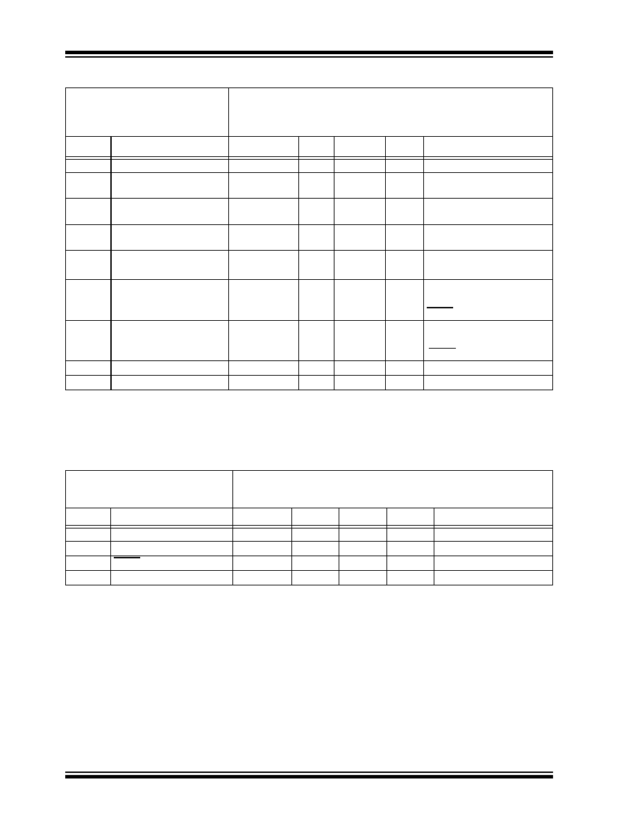
TABLE 4-1:
COMMAND ACTIVATION TIMES
*
These parameters are characterized but not tested.
TABLE 4-2:
DECODER COMMANDS
Decoder State
Min
Max
While receiving transmissions
--
2.5 ms BPW
MAX
= 2.7 ms
During the validation of a received transmission
--
3 ms
During the update of the sync counters
--
40 ms
During learn
--
170 ms
Instruction
Command Byte
Operation
READ
F0
16
Read a byte from user EEPROM
WRITE
E1
16
Write a byte to user EEPROM
ACTIVATE_LRN
D2
16
Activate a learn sequence on the decoder
ERASE_ALL
C3
16
Activate an erase all function on the decoder
PROGRAM
B4
16
Program manufacturer's code and configuration byte
©
2002 Microchip Technology Inc.
DS40153C-page 11
HCS500
4.2.5
READ BYTE/S FROM USER
EEPROM
The read command (Figure 4-4) is used to read bytes
from the user EEPROM. The offset in the user
EEPROM is specified by the address byte which is
truncated to seven bits (C to D). After the address, a
dummy byte must be clocked in (D to E). The EEPROM
data byte is clocked out on the next rising edge of the
clock line with the Least Significant bit first (E to F).
Sequential reads are possible by repeating sequence E
to F within 1 ms after the falling edge of the previous
byte's Most Significant Bit (MSB) bit. During the
sequential read, the address value will wrap after 128
bytes. The decoder will terminate the read command if
no clock pulses are received for a period longer than
1.2 ms.
4.2.6
WRITE BYTE/S TO USER EEPROM
The write command (Figure 4-5) is used to write a loca-
tion in the user EEPROM. The address byte is trun-
cated to seven bits (C to D). The data is clocked in
Least Significant bit first. The clock line must be
asserted to initiate the write. Sequential writes of bytes
are possible by clocking in the byte and then asserting
the clock line (D ≠ F). The decoder will terminate the
write command if no clock pulses are received for a
period longer than 1.2 ms After a successful write
sequence the decoder will acknowledge by taking the
data line high and keeping it high until the clock line
goes low.
FIGURE 4-4:
READ BYTES FROM USER EEPROM
FIGURE 4-5:
WRITE BYTES TO USER EEPROM
Decoder
MSB
A
Command Byte
B
C
LSB
D
T
RD
E
Address Byte
Dummy Byte
CLK
µ
C DATA
F
Data Byte
MSB
LSB
MSB
LSB
MSB
LSB
T
RD
Start Command
DATA
Decoder
MSB
A
Command Byte
Start Command
B
C
LSB
D
T
WR
E
Address Byte
Data Byte
CLK
µ
C DATA
F
Acknowledge
MSB
LSB
MSB
LSB
T
ACK
T
RESP
T
ACK
2
DATA
HCS500
DS40153C-page 12
©
2002 Microchip Technology Inc.
4.2.7
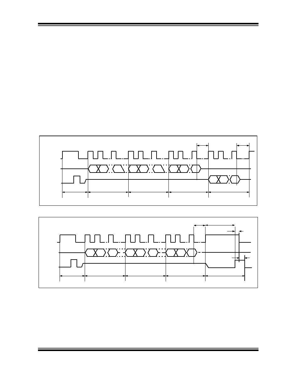
ACTIVATE LEARN
The activate learn command (Figure 4-6) is used to
activate a transmitter learning sequence on the
decoder. The command consists of a Command mode
activation sequence, a command byte, and two dummy
bytes. The decoder will respond by taking the data line
high to acknowledge that the command was valid and
that learn is active.
Upon reception of the first transmission, the decoder
will respond with a learn status message (Figure 4-7).
During learn, the decoder will acknowledge the recep-
tion of the first transmission by taking the data line high
for 60 ms. The controlling microcontroller can clock out
at most eight bits, which will all be zeros. All of the bits
of the status byte are zero, and this is used to distin-
guish between a learn time-out status string and the
first transmission received string. The controlling micro-
controller must ensure that the clock line does not go
high 60 ms after the falling edge of the data line, for this
will terminate learn.
Upon reception of the second transmission, the
decoder will respond with a learn status message
(Figure 4-8).
The learn status message after the second transmis-
sion consists of the following:
∑ 1 START bit.
∑ The function code [S3:S0] of the message is zero,
indicating that this is a status string.
∑ The RESULT bit indicates the result of the learn
sequence. The RESULT bit is set if successful
and cleared otherwise.
∑ The OVR bit will indicate whether an exiting trans-
mitter is over written. The OVR bit will be set if an
existing transmitter is learned over.
∑ The [CNT3...CNT0] bits will indicate the number
of transmitters learned on the decoder.
∑ The [TX3...TX0] bits indicate the block number
used during the learning of the transmitter.
FIGURE 4-6:
LEARN MODE ACTIVATION
FIGURE 4-7:
LEARN STATUS MESSAGE AFTER FIRST TRANSMISSION
FIGURE 4-8:
LEARN STATUS MESSAGE AFTER SECOND TRANSMISSION
Decoder
MSB
A
Command Byte
Start Command
B
C
LSB
D
T
LRN
E
Dummy Byte
Dummy Byte
CLK
µ
C DATA
F
Acknowledge
MSB
LSB
MSB
LSB
T
ACK
T
RESP
T
ACK
2
DATA
Command Request
T
CLKL
T
CLKH
T
CA
T
DS
A
B
T
CLL
T
DHI
T
CLA
T
CLH
CLK
Decoder
0
0
0
0
0
0
0
0
Status Byte
C
Data
Communications Request
T
CLKL
T
CLKH
T
CA
T
DS
A
B
Cii
T
CLL
T
DHI
T
CLA
T
CLH
CLK
Decoder
TX0
TX3
RX63
OVR RSLT
0
0
0
0
CNT0
CNT3
0
RX0
RX1
RX62
1
Ci
Learn Status Bits
Decoded Tx
Data
©
2002 Microchip Technology Inc.
DS40153C-page 13
HCS500
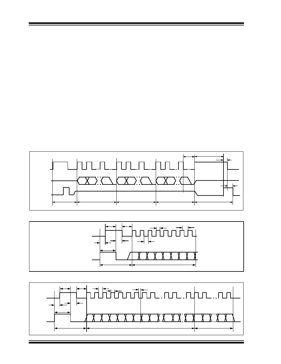
4.2.8
ERASE ALL
The erase all command (Figure 4-9) erases all the
transmitters in the decoder. After the command and two
dummy bytes are clocked in, the clock line must be
asserted to activate the command. After a successful
completion of an erase all command, the data line is
asserted until the clock line goes low.
4.3
Stand-alone Mode
The HCS500 decoder can also be used in stand-alone
applications. The HCS500 will activate the data line for
up to 500 ms if a valid transmission was received, and
this output can be used to drive a relay circuit. To acti-
vate learn or erase all commands, a button must be
connected to the CLK input. User feedback is indicated
on an LED connected to the DATA output line. If the
CLK line is pulled high, using the learn button, the LED
will switch on. After the CLK line is kept high for longer
than 2 seconds, the decoder will switch the LED line off,
indicating that learn will be entered if the button is
released. If the CLK line is kept high for another 6 sec-
onds, the decoder will activate an ERASE_ALL Com-
mand.
Learn mode can be aborted by taking the clock line
high until the data line goes high (LED switches on).
During learn, the data line will give feedback to the user
and, therefore, must not be connected to the relay drive
circuitry.
After taking the clock low and before a transmitter is
learn, any low-to-high change on the clock line may ter-
minate learn. This has learn implications when a switch
with contact bounce is used.
4.4
Erase All Command and Erase
Command
The Table 4-3 describes two versions of the Erase All
command.
Subcommand 01 can be used where a transmitter with
permanent status is implemented in the microcontroller
software. Use of subcommand 01 ensures that the per-
manent transmitter remains in memory even when all
other transmitters are erased. The first transmitter
learned after any of the following events is the first
transmitter in memory and becomes the permanent
transmitter:
1.
Programming of the manufacturer's code.
2.
Erasing of all transmitters
(subcommand 00 only).
4.5
Test mode
A special test mode is activated after:
1.
Programming of the manufacturer's code.
2.
Erasing of all transmitters.
Test mode can be used to test a decoder before any
transmitters are learned on it. Test mode enables test-
ing of decoders without spending the time to learn a
transmitter. Test mode is terminated after the first suc-
cessful learning of an ordinary transmitter. In test
mode, the decoder responds to a test transmitter. The
test transmitter has the following properties:
1.
crypt key = manufacturer's code.
2.
Serial number = any value.
3.
Discrimination bits = lower 10 bits of the serial
number.
4.
Synchronization counter value = any value
(synchronization information is ignored).
Because the synchronization counter value is ignored
in test mode, any number of test transmitters can be
used, even if their synchronization counter values are
different.
4.6
Power Supply Supervisor
Reliable operation of the HCS500 requires that the
contents of the EEPROM memory be protected against
erroneous writes. To ensure that erroneous writes do
not occur after supply voltage "brown-out" conditions,
the use of a proper power supply supervisor device
(like Microchip part MCP100-450) is imperative.
Note:
The REPS bit must be cleared in the con-
figuration byte in Stand-alone mode.
TABLE 4-3:
ERASE ALL COMMAND
Command
Byte
Subcommand
Byte
Description
C3
16
00
16
Erase all
transmitters.
C3
16
01
16
Erase all transmit-
ters except 1. The
first transmitter in
memory is not
erased.
HCS500
DS40153C-page 14
©
2002 Microchip Technology Inc.
FIGURE 4-9:
ERASE ALL
FIGURE 4-10: STAND-ALONE MODE LEARN/ERASE-ALL TIMING
FIGURE 4-11: TYPICAL STAND-ALONE APPLICATION CIRCUIT
Decoder
MSB
A
Command Byte
Start Command
B
C
LSB
D
T
ERA
E
Subcommand Byte
Dummy Byte
CLK
F
Acknowledge
MSB
LSB
MSB
LSB
T
ACK
T
RESP
T
ACK
2
DATA
µ
C DATA
DATA
A
Erase-All Activation
T
PP
1
T
PP
2
CLK
B
C
D
Learn Activation
T
PP
3
Successful
E
T
PP
4
OUTPUT
RELAY SPST
Vcc
Vcc
LEARN
V
CC
1K
A0
1
A1
2
A2
3
V
SS
4
SDA 5
SCL 6
WP 7
V
CC
8
24LC02B
V
DD
1
EECLK
2
EEDAT
3
MCLR
4
SDAT 5
SCLK 6
RFIN 7
V
SS
8
HCS500
NPN
10K
LED
10K
10K
V
CC
Vi
RST
Power Supply
RF
Receiver
Supervisor
22
µ
F
Note:
Because each HCS500 is individually matched to its EEPROM, in-circuit programming is
strongly recommended.
In-circuit
Programming
Probe Pads (Note)
MCP100-4.5

©
2002 Microchip Technology Inc.
DS40153C-page 15
HCS500
5.0
DECODER PROGRAMMING
The decoder uses a 2K, 24LC02B serial EEPROM. The memory is divided between system memory that stores the
transmitter information (read protected) and user memory (read/write). Commands to access the user memory are
described in Sections 4.2.5 and 4.2.6.
The following information stored in system memory needs to be programmed before the decoder can be used:
∑ 64-bit manufacturer's code
∑ Decoder configuration byte
5.1
Configuration Byte
The decoder is configured during initialization by setting the appropriate bits in the configuration byte. The following table
list the options:
5.1.1
LRN_MODE
LRN_MODE selects between two learning modes. With LRN_MODE = 0, the Normal (serial number derived) mode is
selected; with LRN_MODE=1, the Secure (seed derived) mode is selected. See Section 6.0 for more detail on learning
modes.
5.1.2
LRN_ALG
LRN_ALG selects between the two available algorithms. With LRN_ALG = 0, is selected the K
EE
L
OQ
decryption
algorithm is selected; with LRN_ALG = 1, the XOR algorithm is selected. See Section 6.0 for more detail on learning
algorithms.
5.1.3
REPEAT
The HCS500 can be configured to indicate repeated transmissions. In a stand-alone configuration, repeated transmis-
sions must be disabled.
Note 1: These memory locations are read protected and can only be written to using the program command with
the device powered up.
2: The contents of the system memory is encrypted by a unique 64-bit key that is stored in the HCS500. To
initialize the system memory, the HCS500's program command must be used. The EEPROM and HCS500
are matched, and the devices must be kept together. In-circuit programming is therefore recommended.
Bit
Mnemonic
Description
0
LRN_MODE
Learning mode selection
LRN_MODE = 0--Normal Learn
LRN_MODE = 1--Secure Learn
1
LRN_ALG
Algorithm selection
LRN_ALG = 0--K
EE
L
OQ
Decryption Algorithm
LRN_ALG = 1--XOR Algorithm
2
REPEAT
Repeat Transmission enable
0 = Disable
1 = Enabled
3
Not Used
Reserved
4
Not Used
Reserved
5
Not Used
Reserved
6
Not Used
Reserved
7
Not Used
Reserved
HCS500
DS40153C-page 16
©
2002 Microchip Technology Inc.
5.2
Programming Waveform
The programming command consists of the following:
∑ Command Request Sequence (A to B)
∑ Command Byte (B to C)
∑ Configuration Byte (C to D)
∑ Manufacturer's Code Eight Data Bytes (D to G)
∑ Activation and Acknowledge Sequence (G to H)
5.3
Programming Data String
A total of 80 bits are clocked into the decoder. The 8-bit
command byte is clocked in first, followed by the 8-bit
configuration byte and the 64-bit manufacturer's code.
The data must be clocked in Least Significant Bit (LSB)
first. The decoder will then encrypt the manufacturer's
code using the decoder's unique 64-bit EEPROM crypt
key. After completion of the programming EEPROM,
the decoder will acknowledge by taking the data line
high (G to H). If the data line goes high within 30 ms
after the clock goes high, programming also fails.
FIGURE 5-1:
PROGRAMMING WAVEFORM
DECODER
MSB
MSB
A
Command Byte
Start Command
T
CLKL
T
CLKH
T
PP
1
T
DS
B
C
LSB
T
PP
3
T
PP
2
T
CMD
D
LSB
LSB
Configuration Byte
CLK
µ
C DATA
MSB
T
DATA
G
Most Significant Byte
H
T
ACK
T
WT
2
T
AW
Acknowledge
MSB
E
Least Significant Byte
F
T
DATA
T
ADDR
T
PP
4
DATA

©
2002 Microchip Technology Inc.
DS40153C-page 17
HCS500
6.0
KEY GENERATION
The HCS500 supports three learning schemes which are selected during the initialization of the system EEPROM. The
learning schemes are:
∑ Normal learn using the K
EE
L
OQ
decryption algorithm
∑ Secure learn using the K
EE
L
OQ
decryption algorithm
∑ Secure learn using the XOR algorithm
6.1
Normal (Serial Number derived) Learn using the K
EE
L
OQ
Decryption Algorithm
This learning scheme uses the K
EE
L
OQ
decryption algorithm and the 28-bit serial number of the transmitter to derive
the crypt key. The 28-bit serial number is patched with predefined values as indicated below to form two 32-bit seeds.
SourceH = 60000000 00000000H + Serial Number |
28 Bits
SourceL = 20000000 00000000H + Serial Number |
28 Bits
Then, using the K
EE
L
OQ
decryption algorithm and the manufacturer's code the crypt key is derived as follows:
KeyH
Upper 32 bits
= F
K
EE
L
OQ
Decryption
(SourceH) |
64-Bit Manufacturer's Code
KeyL
Lower 32 bits
= F
K
EE
L
OQ
Decryption
(SourceL) |
64-Bit Manufacturer's Code
6.2
Secure (Seed Derived) Learn using the K
EE
L
OQ
Decryption Algorithm
This scheme uses the secure seed transmitted by the encoder to derive the two input seeds. The decoder always uses
the lower 64 bits of the transmission to form a 60-bit seed. The upper 4 bits are always forced to zero.
For 32-bit seed encoders (HCS200, HCS201, HCS300, HCS301):
SourceH = Serial Number
Lower 28 bits
SourceL = Seed
32 bits
For 48-bit seed encoders (HCS360, HCS361):
SourceH = Serial Number (with upper 4 bits set to zero)
Upper 16 bits
<<16 + Seed
Upper 16 bits
SourceL = Seed
Lower
32 bits
For 60-bit seed encoders (HCS362, HCS365, HCS370, HCS410, HCS412, HCS473):
SourceH = Seed
Upper 32 bits
(with upper 4 bits set to zero)
SourceL = Seed
Lower 32 bits
The K
EE
L
OQ
decryption algorithm and the manufacturer's code is used to derive the crypt key as follows:
KeyH
Upper 32 bits
= Decrypt
(SourceH)
64 Bit Manufacturer's Code
KeyL
Lower 32 bits
= Decrypt (SourceL)
64 Bit Manufacturer's Code
6.3
Secure (Seed Derived) Learn using the XOR Algorithm
This scheme uses the seed transmitted by the encoder to derive the two input seeds. The decoder always use the lower
64 bits of the transmission to form a 60-bit seed. The upper 4 bits are always forced to zero.
For 32-bit seed encoders (HCS200, HCS201, HCS300, HCS301):
SourceH = Serial Number
Lower 28 bits
SourceL = Seed
32 bits
For 48-bit seed encoders (HCS360/HCS361):
SourceH = Serial Number (with upper 4 bits set to zero)
Upper 16 bits
<<16 + Seed
Upper 16 bits
SourceL = Seed
Lower 32 bits
For 60-bit seed encoders (HCS362, HCS365, HCS370, HCS410, HCS412, HCS473):
SourceH = Seed
Upper 32 bits
with upper 4 bits set to zero
SourceL = Seed
Lower 32 bits
Then, using the manufacturer's code the crypt key is derived as follows:
KeyH
Upper 32 bits
= SourceH XOR 64-Bit Manufacturer's Code
Upper 32 bits
KeyL
Lower 32 bits
= SourceL XOR 64-Bit Manufacturer's Code
Lower 32 bits
HCS500
DS40153C-page 18
©
2002 Microchip Technology Inc.
7.0
K
EE
L
OQ
ENCODERS
7.1
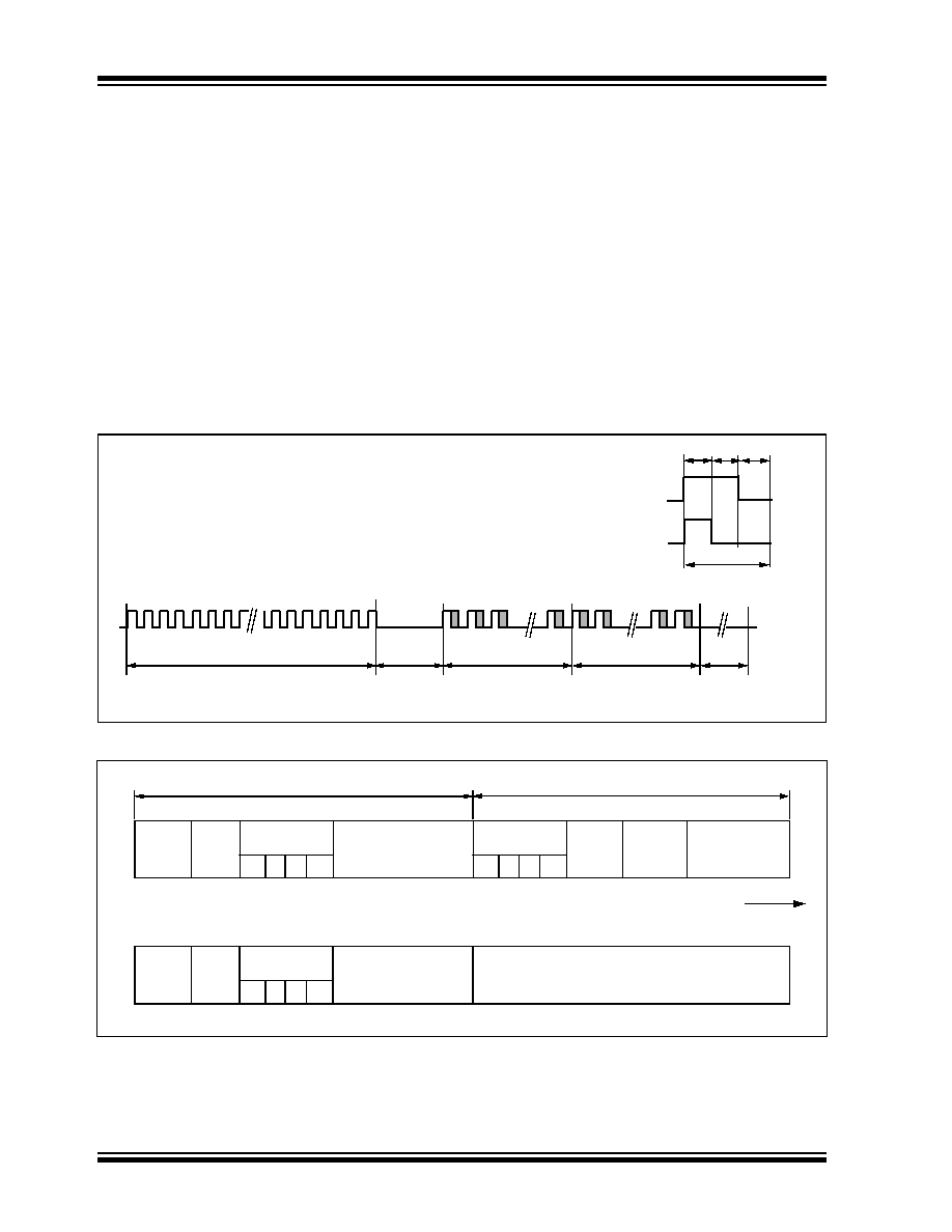
Transmission Format (PWM)
The K
EE
L
OQ
encoder transmission is made up of sev-
eral parts (Figure 7-1). Each transmission begins with
a preamble and a header, followed by the encrypted
and then the fixed data. The actual data is 66/69 bits
which consists of 32 bits of encrypted data and 34/35
bits of non-encrypted data. Each transmission is fol-
lowed by a guard period before another transmission
can begin. The code hopping portion provides up to
four billion changing code combinations and includes
the button status bits (based on which buttons were
activated), along with the synchronization counter
value and some discrimination bits. The non-code hop-
ping portion is comprised of the status bits, the function
bits, and the 28-bit serial number. The encrypted and
non-encrypted combined sections increase the number
of combinations to 7.38 x 10
19
.
7.2
Code Word Organization
The HCS encoder transmits a 66/69-bit code word
when a button is pressed. The 66/69-bit word is con-
structed from a code hopping portion and a non-code
hopping portion (Figure 7-2).
The Encrypted Data is generated from four button bits,
two overflow counter bits, ten discrimination bits, and
the 16-bit synchronization counter value.
The Non-encrypted Data is made up from 2 status
bits, 4 function bits, and the 28/32-bit serial number.
FIGURE 7-1:
TRANSMISSION FORMAT (PWM)
FIGURE 7-2:
CODE WORD ORGANIZATION
LOGIC "1"
Guard
Time
50%
Encrypted
Portion
Fixed Code
Portion
LOGIC "0"
Preamble
Header
T
E
T
E
T
E
10xT
E
T
BP
Repeat
(1-bit)
V
LOW
(1-bit)
Button
Status
S2 S1 S0 S3
Serial Number
(28 bits)
Button
Status
S2 S1 S0 S3
OVR
(2 bits)
DISC
(10 bits)
Sync Counter
(16 bits)
Repeat
(1-bit)
V
LOW
(1-bit)
Button
Status
1 1 1 1
Serial Number
(28 bits)
SEED
(32 bits)
34 bits of Fixed Portion
32 bits of Encrypted Portion
66 Data bits
Transmitted
LSb first.
LSb
MSb
MSb
LSb
SEED replaces Encrypted Portion when all button inputs are activated at the same time.

©
2002 Microchip Technology Inc.
DS40153C-page 19
HCS500
8.0
ELECTRICAL CHARACTERISTICS FOR HCS500
Absolute Maximum Ratings
Ambient temperature under bias............................................................................................................ -40∞C to +125∞C
Storage temperature .............................................................................................................................. -65 ∞C to +150∞C
Voltage on any pin with respect to V
SS
(except V
DD
)......................................................................... -0.6V to V
DD
+0.6V
Voltage on V
DD
with respect to Vss ..................................................................................................................0 to +7.5V
Total power dissipation (Note) ............................................................................................................................. 700 mW
Maximum current out of V
SS
pin ...........................................................................................................................200 mA
Maximum current into V
DD
pin .............................................................................................................................. 150 mA
Input clamp current, I
IK
(V
I
< 0 or V
I
> V
DD
) ......................................................................................................... ± 20 mA
Output clamp current, IOK (V
O
< 0 or V
O
>V
DD
) .................................................................................................. ± 20 mA
Maximum output current sunk by any I/O pin..........................................................................................................25 mA
Maximum output current sourced by any I/O pin .................................................................................................... 25 mA
Note:
Power dissipation is calculated as follows: P
DIS
= V
DD
x {I
DD
-
I
OH
} +
{(V
DD
≠V
OH
) x I
OH
} +
(V
O
l x I
OL
)
NOTICE: Stresses above those listed under "Absolute Maximum Ratings" may cause permanent damage to the
device. This is a stress rating only and functional operation of the device at those or any other conditions above
those indicated in the operation listings of this specification is not implied. Exposure to maximum rating conditions for
extended periods may affect device reliability.
HCS500
DS40153C-page 20
©
2002 Microchip Technology Inc.
TABLE 8-1:
DC CHARACTERISTICS
Standard Operating Conditions (unless otherwise stated)
Operating temperature
Commercial (C):
0∞C
T
A
+70∞C
Industrial (I):
-40∞C
T
A
+85∞C
Symbol
Parameters
Min
Typ
()
Max
Units
Conditions
V
DD
Supply voltage
3.0
--
5.5
V
V
POR
V
DD
start voltage to
ensure RESET
--
Vss
--
V
S
VDD
V
DD
rise rate to
ensure RESET
0.05*
--
--
V/ms
I
DD
Supply current
--
--
1.8
0.3
2.4
5
mA
µ
A
F
OSC
= 4 MHz, V
DD
= 5.5V
SLEEP mode (no RF input)
I
PD
Power-Down Current
--
0.25
4
µ
A
V
DD
= 3.0V, Commercial
--
0.3
5
µ
A
V
DD
= 3.0V, Industrial
V
IL
Input low voltage
V
SS
V
SS
--
--
0.8
0.15 V
DD
V
V
V
DD
between 4.5V and 5.5V
Otherwise
V
SS
--
0.15 V
DD
V
MCLR
V
IH
Input high voltage
2.0
0.25 V
DD
+ 0.8
--
--
V
DD
V
DD
V
V
V
DD
between 4.5V and 5.5V
Otherwise
0.85 V
DD
--
V
DD
V
MCLR
V
OL
Output low voltage
--
--
0.6
V
I
OL
= 8.7 mA, V
DD
= 4.5V
V
OH
Output high voltage
V
DD
- 0.7
--
--
V
I
OH
= -5.4 mA, V
DD
= 4.5V
Data in "Typ" column is at 5.0V, 25
∞
C unless otherwise stated. These parameters are for design guidance only
and are not tested.
*
These parameters are characterized but not tested.
Note:
Negative current is defined as coming out of the pin.
TABLE 8-2:
AC CHARACTERISTICS
Standard Operating Conditions (unless otherwise specified):
Commercial (C):
0∞C
TA
+70∞C
Industrial (I):
-40∞C
TA
+85∞C
Symbol
Parameters
Min
Typ
Max
Units
Conditions
T
E
Transmit elemental period
65
--
660
µ
s
T
OD
Output delay
48
75
237
ms
T
MCLR
MCLR low time
150
--
--
ns
T
OV
Time output valid
--
150
222
ms
*
These parameters are characterized but not tested.
©
2002 Microchip Technology Inc.
DS40153C-page 21
HCS500
FIGURE 8-1:
RESET WATCHDOG TIMER, OSCILLATOR START-UP TIMER AND POWER-UP
TIMER TIMING
V
DD
MCLR
I/O Pins
Tov
T
MCLR
HCS500
DS40153C-page 22
©
2002 Microchip Technology Inc.
8.1
AC Electrical Characteristics
8.1.1
COMMAND MODE ACTIVATION
8.1.2
READ FROM USER EEPROM COMMAND
8.1.3
WRITE TO USER EEPROM COMMAND
Standard Operating Conditions (unless otherwise specified):
Commercial (C):
0∞C
TA
+70∞C
Industrial (I):
-40∞C
TA
+85∞C
Symbol
Parameters
Min
Typ
Max
Units
T
REQ
Command request time
0.0150
--
500
ms
T
RESP
Microcontroller request
acknowledge time
--
--
1
ms
T
ACK
Decoder acknowledge time
--
--
30
µ
s
T
START
Start Command mode to first
command bit
20
--
1000
µ
s
T
CLKH
Clock high time
20
--
1000
µ
s
T
CLKL
Clock low time
20
--
1000
µ
s
F
CLK
Clock frequency
500
--
25000
Hz
T
DS
Data hold time
14
--
--
µ
s
T
CMD
Command validate time
--
--
10
µ
s
T
ADDR
Address validate time
--
--
10
µ
s
T
DATA
Data validate time
--
--
10
µ
s
*
These parameters are characterized but not tested.
Standard Operating Conditions (unless otherwise specified):
Commercial (C):
0∞C
TA
+70∞C
Industrial (I):
-40∞C TA
+85∞C
Symbol
Parameters
Min
Typ
Max
Units
T
RD
Decoder EEPROM read time
400
--
1500
µ
s
*
These parameters are characterized but not tested.
Standard Operating Conditions (unless otherwise specified):
Commercial (C):
0∞C
TA
+70∞C
Industrial (I):
-40∞C
TA
+85∞C
Symbol
Parameters
Min
Typ
Max
Units
T
WR
Write command activation time
20
--
1000
µ
s
T
ACK
EEPROM write acknowledge time
--
--
10
ms
T
RESP
Microcontroller acknowledge
response time
20
--
1000
µ
s
T
ACK
2
Decoder response
acknowledge time
--
--
10
µ
s
*
These parameters are characterized but not tested.
HCS500
©
2002 Microchip Technology Inc.
DS40153C-page 23
8.1.4
ACTIVATE LEARN COMMAND IN MICRO MODE
8.1.5
ACTIVATE LEARN COMMAND IN STAND-ALONE MODE
8.1.6
LEARN STATUS STRING
Standard Operating Conditions (unless otherwise specified):
Commercial (C):
0∞C
TA
+70 ∞C
Industrial (I):
-40∞C
TA
+85∞C
Symbol
Parameters
Min
Typ
Max
Units
T
LRN
Learn command activation time
20
--
1000
µ
s
T
ACK
Decoder acknowledge time
--
--
20
µ
s
T
RESP
Microcontroller acknowledge
response time
20
--
1000
µ
s
T
ACK
2
Decoder data line low
--
--
10
µ
s
*
These parameters are characterized but not tested.
Standard Operating Conditions (unless otherwise specified):
Commercial (C):
0∞C
TA
+70∞C
Industrial (I):
-40∞C
TA
+85∞C
Symbol
Parameters
Min
Typ
Max
Units
T
PP
1
Command request time
--
--
100
ms
T
PP
2
Learn command activation time
--
--
2
s
T
PP
3
Erase-all command activation time
--
--
6
s
*
These parameters are characterized but not tested.
Standard Operating Conditions (unless otherwise specified):
Commercial (C):
0∞C
TA
+70∞C
Industrial (I):
-40∞C TA
+85∞C
Symbol
Parameters
Min
Typ
Max
Units
T
DHI
Command request time
--
--
500
ms
T
CLA
Microcontroller command
request time
0.005
--
500
ms
T
CA
Decoder request
acknowledge time
--
--
10
µ
s
T
CLH
Clock high hold time
1.2
ms
T
CLL
Clock low hold time
0.020
--
1.2
ms
T
CLKH
Clock high time
20
--
1000
µ
s
T
CLKL
Clock low time
20
--
1000
µ
s
F
CLK
Clock frequency
500
--
25000
Hz
T
DS
Data hold time
--
--
5
µ
s
*
These parameters are characterized but not tested.

HCS500
DS40153C-page 24
©
2002 Microchip Technology Inc.
8.1.7
ERASE ALL COMMAND
8.1.8
PROGRAMMING COMMAND
Standard Operating Conditions (unless otherwise specified):
Commercial (C):
0∞C
TA
+70∞C
Industrial (I):
-40∞C
TA
+85∞C
Symbol
Parameters
Min
Typ
Max
Units
T
ERA
Learn command activation time
20
--
1000
µ
s
T
ACK
Decoder acknowledge time
20
--
210
ms
T
RESP
Microcontroller acknowledge
response time
20
--
1000
µ
s
T
ACK
2
Decoder data line low
--
--
10
µ
s
*
These parameters are characterized but not tested.
Standard Operating Conditions (unless otherwise specified):
Commercial (C):
0∞C
TA
+70∞C
Industrial (I):
-40∞C
TA
+85∞C
Symbol
Parameters
Min
Typ
Max
Units
T
PP
1
Command request time
--
--
500
ms
T
PP
2
Decoder acknowledge time
--
--
1
ms
T
PP
3
Start Command mode to first
command bit
20
--
1000
µ
s
T
PP
4
Data line low before tri-stated
--
--
5
µ
s
T
CLKH
Clock high time
20
--
1000
µ
s
T
CLKL
Clock low time
20
--
1000
µ
s
F
CLK
Clock frequency
500
--
25000
Hz
T
DS
Data hold time
--
--
5
µ
s
T
CMD
Command validate time
--
--
10
µ
s
T
ACK
Command acknowledge time
30
--
240
ms
T
WT
2
Acknowledge respond time
20
--
1000
µ
s
T
ALW
Data low after clock low
--
--
10
µ
s
*
These parameters are characterized but not tested.
©
2002 Microchip Technology Inc.
DS40153C-page 25
HCS500
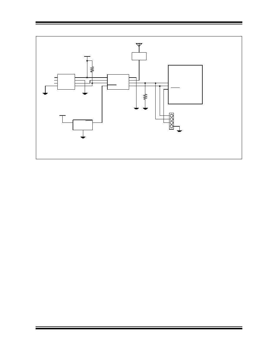
FIGURE 8-2:
TYPICAL MICROCONTROLLER INTERFACE CIRCUIT
V
CC
1K
A0
1
A1
2
A2
3
V
SS
4
SDA 5
SCL 6
WP 7
V
CC
8
24LC02B
V
DD
1
EECLK
2
EEDAT
3
MCLR
4
SDAT 5
SCLK 6
RFIN 7
V
SS
8
HCS500
10K
V
CC
Vi
RST
Power Supply
RF
Receiver
Supervisor
Note:
Because each HCS500 is individually matched to its EEPROM, in-circuit programming is
strongly recommended.
In-circuit
Programming
Probe Pads (Note)
MCP100-4.5
Microcontroller
MCLR
DATA
CLOCK
HCS500
DS40153C-page 26
©
2002 Microchip Technology Inc.
9.0
PACKAGING INFORMATION
9.1
Package Marking Information
8-Lead PDIP (300 mil)
Example
8-Lead SOIC (150 mil)
Example
XXXXXXXX
XXXXXNNN
YYWW
HCS500
XXXXXNNN
0025
XXXXXXX
XXXYYWW
NNN
HCS500
XXX0025
NNN
Legend: XX...X
Customer specific information*
Y
Year code (last digit of calendar year)
YY
Year code (last 2 digits of calendar year)
WW
Week code (week of January 1 is week `01')
NNN
Alphanumeric traceability code
Note:
In the event the full Microchip part number cannot be marked on one line, it will
be carried over to the next line thus limiting the number of available characters
for customer specific information.
*
Standard PICmicro device marking consists of Microchip part number, year code, week code, and
traceability code. For PICmicro device marking beyond this, certain price adders apply. Please check
with your Microchip Sales Office. For QTP devices, any special marking adders are included in QTP
price.
©
2002 Microchip Technology Inc.
DS40153C-page 27
HCS500
9.2
Package Details
8-Lead Plastic Dual In-line (P) - 300 mil (PDIP)
B1
B
A1
A
L
A2
p
E
eB
c
E1
n
D
1
2
Units
INCHES*
MILLIMETERS
Dimension Limits
MIN
NOM
MAX
MIN
NOM
MAX
Number of Pins
n
8
8
Pitch
p
.100
2.54
Top to Seating Plane
A
.140
.155
.170
3.56
3.94
4.32
Molded Package Thickness
A2
.115
.130
.145
2.92
3.30
3.68
Base to Seating Plane
A1
.015
0.38
Shoulder to Shoulder Width
E
.300
.313
.325
7.62
7.94
8.26
Molded Package Width
E1
.240
.250
.260
6.10
6.35
6.60
Overall Length
D
.360
.373
.385
9.14
9.46
9.78
Tip to Seating Plane
L
.125
.130
.135
3.18
3.30
3.43
Lead Thickness
c
.008
.012
.015
0.20
0.29
0.38
Upper Lead Width
B1
.045
.058
.070
1.14
1.46
1.78
Lower Lead Width
B
.014
.018
.022
0.36
0.46
0.56
Overall Row Spacing
ß
eB
.310
.370
.430
7.87
9.40
10.92
Mold Draft Angle Top
5
10
15
5
10
15
Mold Draft Angle Bottom
5
10
15
5
10
15
* Controlling Parameter
Notes:
Dimensions D and E1 do not include mold flash or protrusions. Mold flash or protrusions shall not exceed
JEDEC Equivalent: MS-001
Drawing No. C04-018
.010" (0.254mm) per side.
ß Significant Characteristic
HCS500
DS40153C-page 28
©
2002 Microchip Technology Inc.
8-Lead Plastic Small Outline (SM) - Medium, 208 mil (SOIC)
Foot Angle
0
4
8
0
4
8
15
12
0
15
12
0
Mold Draft Angle Bottom
15
12
0
15
12
0
Mold Draft Angle Top
0.51
0.43
0.36
.020
.017
.014
B
Lead Width
0.25
0.23
0.20
.010
.009
.008
c
Lead Thickness
0.76
0.64
0.51
.030
.025
.020
L
Foot Length
5.33
5.21
5.13
.210
.205
.202
D
Overall Length
5.38
5.28
5.11
.212
.208
.201
E1
Molded Package Width
8.26
7.95
7.62
.325
.313
.300
E
Overall Width
0.25
0.13
0.05
.010
.005
.002
A1
Standoff
ß
1.98
.078
A2
Molded Package Thickness
2.03
.080
A
Overall Height
1.27
.050
p
Pitch
8
8
n
Number of Pins
MAX
NOM
MIN
MAX
NOM
MIN
Dimension Limits
MILLIMETERS
INCHES*
Units
A2
A
A1
L
c
2
1
D
n
p
B
E
E1
.070
.075
.069
.074
1.78
1.75
1.97
1.88
* Controlling Parameter
Notes:
Dimensions D and E1 do not include mold flash or protrusions. Mold flash or protrusions shall not exceed
.010" (0.254mm) per side.
Drawing No. C04-056
ß Significant Characteristic

©
2002 Microchip Technology Inc.
DS40153C-page 29
HCS500
ON-LINE SUPPORT
Microchip provides on-line support on the Microchip
World Wide Web (WWW) site.
The web site is used by Microchip as a means to make
files and information easily available to customers. To
view the site, the user must have access to the Internet
and a web browser, such as Netscape or Microsoft
Explorer. Files are also available for FTP download
from our FTP site.
Connecting to the Microchip Internet Web Site
The Microchip web site is available by using your
favorite Internet browser to attach to:
www.microchip.com
The file transfer site is available by using an FTP ser-
vice to connect to:
ftp://ftp.microchip.com
The web site and file transfer site provide a variety of
services. Users may download files for the latest
Development Tools, Data Sheets, Application Notes,
User's Guides, Articles and Sample Programs. A vari-
ety of Microchip specific business information is also
available, including listings of Microchip sales offices,
distributors and factory representatives. Other data
available for consideration is:
∑ Latest Microchip Press Releases
∑ Technical Support Section with Frequently Asked
Questions
∑ Design Tips
∑ Device Errata
∑ Job Postings
∑ Microchip Consultant Program Member Listing
∑ Links to other useful web sites related to
Microchip Products
∑ Conferences for products, Development Systems,
technical information and more
∑ Listing of seminars and events
Systems Information and Upgrade Hot Line
The Systems Information and Upgrade Line provides
system users a listing of the latest versions of all of
Microchip's development systems software products.
Plus, this line provides information on how customers
can receive any currently available upgrade kits.The
Hot Line Numbers are:
1-800-755-2345 for U.S. and most of Canada, and
1-480-792-7302 for the rest of the world.

HCS500
DS40153C-page 30
©
2002 Microchip Technology Inc.
READER RESPONSE
It is our intention to provide you with the best documentation possible to ensure successful use of your Microchip prod-
uct. If you wish to provide your comments on organization, clarity, subject matter, and ways in which our documentation
can better serve you, please FAX your comments to the Technical Publications Manager at (480) 792-4150.
Please list the following information, and use this outline to provide us with your comments about this Data Sheet.
To:
Technical Publications Manager
RE:
Reader Response
Total Pages Sent
From: Name
Company
Address
City / State / ZIP / Country
Telephone: (_______) _________ - _________
Application (optional):
Would you like a reply? Y N
Device:
Literature Number:
Questions:
FAX: (______) _________ - _________
DS40153C
HCS500
1.
What are the best features of this document?
2.
How does this document meet your hardware and software development needs?
3.
Do you find the organization of this data sheet easy to follow? If not, why?
4.
What additions to the data sheet do you think would enhance the structure and subject?
5.
What deletions from the data sheet could be made without affecting the overall usefulness?
6.
Is there any incorrect or misleading information (what and where)?
7.
How would you improve this document?
8.
How would you improve our software, systems, and silicon products?
©
2002 Microchip Technology Inc.
DS40153C-page 31
HCS500
HCS500 PRODUCT IDENTIFICATION SYSTEM
To order or obtain information, e.g., on pricing or delivery, refer to the factory or the listed sales office.
Sales and Support
Package:
P = Plastic DIP (300 mil Body), 8-lead
SM = Plastic SOIC (207 mil Body), 8-lead
Temperature
Blank = 0∞C to +70∞C
Range:
I
= ≠40∞C to +85∞C
Device:
HCS500
Code Hopping Decoder
HCS500T
Code Hopping Decoder (Tape and Reel)
HCS500
--
/P
Data Sheets
Products supported by a preliminary Data Sheet may have an errata sheet describing minor operational differences and recom-
mended workarounds. To determine if an errata sheet exists for a particular device, please contact one of the following:
1.
Your local Microchip sales office
2.
The Microchip Corporate Literature Center U.S. FAX: (480) 792-7277
3.
The Microchip Worldwide Site (www.microchip.com)
Please specify which device, revision of silicon and Data Sheet (include Literature #) you are using.
New Customer Notification System
Register on our web site (www.microchip.com/cn) to receive the most current information on our products.

HCS500
DS40153C-page 32
©
2002 Microchip Technology Inc.
NOTES:

©
2002 Microchip Technology Inc.
DS40153C - page 33
Information contained in this publication regarding device
applications and the like is intended through suggestion only
and may be superseded by updates. It is your responsibility to
ensure that your application meets with your specifications.
No representation or warranty is given and no liability is
assumed by Microchip Technology Incorporated with respect
to the accuracy or use of such information, or infringement of
patents or other intellectual property rights arising from such
use or otherwise. Use of Microchip's products as critical com-
ponents in life support systems is not authorized except with
express written approval by Microchip. No licenses are con-
veyed, implicitly or otherwise, under any intellectual property
rights.
Trademarks
The Microchip name and logo, the Microchip logo, FilterLab,
K
EE
L
OQ
, MPLAB, PIC, PICmicro, PICMASTER, PICSTART,
PRO MATE, SEEVAL and The Embedded Control Solutions
Company are registered trademarks of Microchip Technology
Incorporated in the U.S.A. and other countries.
dsPIC, ECONOMONITOR, FanSense, FlexROM, fuzzyLAB,
In-Circuit Serial Programming, ICSP, ICEPIC, microID,
microPort, Migratable Memory, MPASM, MPLIB, MPLINK,
MPSIM, MXDEV, PICC, PICDEM, PICDEM.net, rfPIC, Select
Mode and Total Endurance are trademarks of Microchip
Technology Incorporated in the U.S.A.
Serialized Quick Turn Programming (SQTP) is a service mark
of Microchip Technology Incorporated in the U.S.A.
All other trademarks mentioned herein are property of their
respective companies.
© 2002, Microchip Technology Incorporated, Printed in the
U.S.A., All Rights Reserved.
Printed on recycled paper.
Microchip received QS-9000 quality system
certification for its worldwide headquarters,
design and wafer fabrication facilities in
Chandler and Tempe, Arizona in July 1999. The
Company's quality system processes and
procedures are QS-9000 compliant for its
PICmicro
Æ
8-bit MCUs, K
EE
L
OQ
Æ
code hopping
devices, Serial EEPROMs and microperipheral
products. In addition, Microchip's quality
system for the design and manufacture of
development systems is ISO 9001 certified.
Microchip's Secure Data Products are covered by some or all of the following patents:
Code hopping encoder patents issued in Europe, U.S.A., and R.S.A. -- U.S.A.: 5,517,187; Europe: 0459781; R.S.A.: ZA93/4726
Secure learning patents issued in the U.S.A. and R.S.A. -- U.S.A.: 5,686,904; R.S.A.: 95/5429

DS40153C-page 34
©
2002 Microchip Technology Inc.
AMERICAS
Corporate Office
2355 West Chandler Blvd.
Chandler, AZ 85224-6199
Tel: 480-792-7200 Fax: 480-792-7277
Technical Support: 480-792-7627
Web Address: http://www.microchip.com
Rocky Mountain
2355 West Chandler Blvd.
Chandler, AZ 85224-6199
Tel: 480-792-7966 Fax: 480-792-7456
Atlanta
500 Sugar Mill Road, Suite 200B
Atlanta, GA 30350
Tel: 770-640-0034 Fax: 770-640-0307
Boston
2 Lan Drive, Suite 120
Westford, MA 01886
Tel: 978-692-3848 Fax: 978-692-3821
Chicago
333 Pierce Road, Suite 180
Itasca, IL 60143
Tel: 630-285-0071 Fax: 630-285-0075
Dallas
4570 Westgrove Drive, Suite 160
Addison, TX 75001
Tel: 972-818-7423 Fax: 972-818-2924
Detroit
Tri-Atria Office Building
32255 Northwestern Highway, Suite 190
Farmington Hills, MI 48334
Tel: 248-538-2250 Fax: 248-538-2260
Kokomo
2767 S. Albright Road
Kokomo, Indiana 46902
Tel: 765-864-8360 Fax: 765-864-8387
Los Angeles
18201 Von Karman, Suite 1090
Irvine, CA 92612
Tel: 949-263-1888 Fax: 949-263-1338
New York
150 Motor Parkway, Suite 202
Hauppauge, NY 11788
Tel: 631-273-5305 Fax: 631-273-5335
San Jose
Microchip Technology Inc.
2107 North First Street, Suite 590
San Jose, CA 95131
Tel: 408-436-7950 Fax: 408-436-7955
Toronto
6285 Northam Drive, Suite 108
Mississauga, Ontario L4V 1X5, Canada
Tel: 905-673-0699 Fax: 905-673-6509
ASIA/PACIFIC
Australia
Microchip Technology Australia Pty Ltd
Suite 22, 41 Rawson Street
Epping 2121, NSW
Australia
Tel: 61-2-9868-6733 Fax: 61-2-9868-6755
China - Beijing
Microchip Technology Consulting (Shanghai)
Co., Ltd., Beijing Liaison Office
Unit 915
Bei Hai Wan Tai Bldg.
No. 6 Chaoyangmen Beidajie
Beijing, 100027, No. China
Tel: 86-10-85282100 Fax: 86-10-85282104
China - Chengdu
Microchip Technology Consulting (Shanghai)
Co., Ltd., Chengdu Liaison Office
Rm. 2401, 24th Floor,
Ming Xing Financial Tower
No. 88 TIDU Street
Chengdu 610016, China
Tel: 86-28-6766200 Fax: 86-28-6766599
China - Fuzhou
Microchip Technology Consulting (Shanghai)
Co., Ltd., Fuzhou Liaison Office
Unit 28F, World Trade Plaza
No. 71 Wusi Road
Fuzhou 350001, China
Tel: 86-591-7503506 Fax: 86-591-7503521
China - Shanghai
Microchip Technology Consulting (Shanghai)
Co., Ltd.
Room 701, Bldg. B
Far East International Plaza
No. 317 Xian Xia Road
Shanghai, 200051
Tel: 86-21-6275-5700 Fax: 86-21-6275-5060
China - Shenzhen
Microchip Technology Consulting (Shanghai)
Co., Ltd., Shenzhen Liaison Office
Rm. 1315, 13/F, Shenzhen Kerry Centre,
Renminnan Lu
Shenzhen 518001, China
Tel: 86-755-2350361 Fax: 86-755-2366086
Hong Kong
Microchip Technology Hongkong Ltd.
Unit 901-6, Tower 2, Metroplaza
223 Hing Fong Road
Kwai Fong, N.T., Hong Kong
Tel: 852-2401-1200 Fax: 852-2401-3431
India
Microchip Technology Inc.
India Liaison Office
Divyasree Chambers
1 Floor, Wing A (A3/A4)
No. 11, O'Shaugnessey Road
Bangalore, 560 025, India
Tel: 91-80-2290061 Fax: 91-80-2290062
Japan
Microchip Technology Japan K.K.
Benex S-1 6F
3-18-20, Shinyokohama
Kohoku-Ku, Yokohama-shi
Kanagawa, 222-0033, Japan
Tel: 81-45-471- 6166 Fax: 81-45-471-6122
Korea
Microchip Technology Korea
168-1, Youngbo Bldg. 3 Floor
Samsung-Dong, Kangnam-Ku
Seoul, Korea 135-882
Tel: 82-2-554-7200 Fax: 82-2-558-5934
Singapore
Microchip Technology Singapore Pte Ltd.
200 Middle Road
#07-02 Prime Centre
Singapore, 188980
Tel: 65-334-8870 Fax: 65-334-8850
Taiwan
Microchip Technology Taiwan
11F-3, No. 207
Tung Hua North Road
Taipei, 105, Taiwan
Tel: 886-2-2717-7175 Fax: 886-2-2545-0139
EUROPE
Denmark
Microchip Technology Nordic ApS
Regus Business Centre
Lautrup hoj 1-3
Ballerup DK-2750 Denmark
Tel: 45 4420 9895 Fax: 45 4420 9910
France
Microchip Technology SARL
Parc d'Activite du Moulin de Massy
43 Rue du Saule Trapu
Batiment A - ler Etage
91300 Massy, France
Tel: 33-1-69-53-63-20 Fax: 33-1-69-30-90-79
Germany
Microchip Technology GmbH
Gustav-Heinemann Ring 125
D-81739 Munich, Germany
Tel: 49-89-627-144 0 Fax: 49-89-627-144-44
Italy
Microchip Technology SRL
Centro Direzionale Colleoni
Palazzo Taurus 1 V. Le Colleoni 1
20041 Agrate Brianza
Milan, Italy
Tel: 39-039-65791-1 Fax: 39-039-6899883
United Kingdom
Arizona Microchip Technology Ltd.
505 Eskdale Road
Winnersh Triangle
Wokingham
Berkshire, England RG41 5TU
Tel: 44 118 921 5869 Fax: 44-118 921-5820
01/18/02
W
ORLDWIDE
S
ALES
AND
S
ERVICE