
©
1997 Microchip Technology Inc.
DS40151C-page 1
M
HCS512
FEATURES
Security
∑ Secure storage of Manufacturer's Code
∑ Secure storage of transmitter's keys
∑ Up to four transmitters can be learned
∑ K
EE
L
OQ
code hopping technology
∑ Normal and secure learning mechanisms
Operating
∑ 3.0V ≠ 6.0V operation
∑ 4 MHz RC oscillator
∑ Learning indication on LRNOUT
∑ Auto baud rate detection
∑ Power saving sleep mode
Other
∑ Stand alone decoder
∑ On-chip EEPROM for transmitter storage
∑ Four binary function outputs≠15 functions
∑ 18-pin DIP/SOIC package
Typical Applications
∑ Automotive remote entry systems
∑ Automotive alarm systems
∑ Automotive immobilizers
∑ Gate and garage openers
∑ Electronic door locks
∑ Identity tokens
∑ Burglar alarm systems
Compatible Encoders
∑ HCS200, HCS300, HCS301, HCS360, HCS361
∑ NTQ106
DESCRIPTION
The Microchip Technology Inc. HCS512 is a code hop-
ping decoder designed for secure Remote Keyless
Entry (RKE) systems. The HCS512 utilizes the pat-
ented K
EE
L
OQ
code hopping system and high security
learning mechanisms to make this a canned solution
when used with the HCS encoders to implement a uni-
directional remote keyless entry system.
PACKAGE TYPE
BLOCK DIAGRAM
The Manufacturer's Code, transmitter keys, and syn-
chronization information are stored in protected on-chip
EEPROM. The HCS512 uses the DATA and CLK inputs
to load the Manufacturer's Code which cannot be read
out of the device.
The HCS512 operates over a wide voltage range of
3.0 volts to 6.0 volts. The decoder employs automatic
baud rate detection which allows it to compensate for
wide variations in transmitter data rate. The decoder
contains sophisticated error checking algorithms to
ensure only valid codes are accepted.
HCS512
PDIP, SOIC
1
2
3
4
5
6
7
8
9
LRNIN
LRNOUT
NC
MCLR
GND
S0
S1
S2
S3
18
17
16
15
14
13
12
11
10
RFIN
NC
OSCIN
OSC
OUT
V
DD
DATA
CLK
SLEEP
V
LOW
S0
S1
S3
S2
V
LOW
67-Bit Reception Register
EEPROM
CONTROL
DECRYPTOR
OUTPUT
SEL
RFIN
OSCILLATOR
OSCIN
CONTROL
LRNOUT
DATA
CLK
LRNIN
MCLR
SLEEP
Code Hopping Decoder

HCS512
DS40151C-page 2
©
1997 Microchip Technology Inc.
1.0
K
EE
L
OQ
SYSTEM OVERVIEW
1.1
Key Terms
∑ Manufacturer's Code ≠ a 64-bit word, unique to
each manufacturer, used to produce a unique
encoder key in each transmitter (encoder).
∑ Encoder Key ≠ a 64-bit key, unique for each trans-
mitter. The encoder key controls the decryption
algorithm and is stored in EEPROM on the
decoder device.
∑ Learn ≠ The receiver uses information that is
transmitted to derive the transmitter's secret key,
decrypt the discrimination value and the synchro-
nization counter in learning mode. The encoder
key is a function of the Manufacturer's Code and
the device serial number and/or seed value.
The HCS encoders and decoders employ the K
EE
L
OQ
code hopping technology and an encryption algorithm
to achieve a high level of security. Code hopping is a
method by which the code transmitted from the trans-
mitter to the receiver is different every time a button is
pushed. This method, coupled with a transmission
length of 66 bits, virtually eliminates the use of code
`grabbing' or code `scanning'.
1.2
HCS Encoder Overview
The HCS encoders have a small EEPROM array which
must be loaded with several parameters before use.
The most important of these values are:
∑ A 28-bit serial number which is meant to be
unique for every encoder
∑ An encoder key that is generated at the time of
production
∑ A 16-bit synchronization value
The serial number for each encoder is programmed by
the manufacturer at the time of production. The
generation of the encoder key is done using a key gen-
eration algorithm (Figure 1-1). Typically, inputs to the
key generation algorithm are the serial number of the
encoder and a 64-bit manufacturer's code. The manu-
facturer's code is chosen by the system manufacturer
and must be carefully controlled. The manufacturer's
code is a pivotal part of the overall system security.
FIGURE 1-1:
CREATION AND STORAGE OF ENCODER KEY DURING PRODUCTION
Transmitter
Manufacturer's
Serial Number or
Code
Encoder
Key
Key
Generation
Algorithm
Serial Number
Encoder Key
Sync Counter
.
.
.
HCSXXX EEPROM Array
Seed

HCS512
©
1997 Microchip Technology Inc.
DS40151C-page 3
The 16-bit synchronization value is the basis for the
transmitted code changing for each transmission and is
updated each time a button is pressed. Because of the
complexity of the code hopping encryption algorithm, a
change in one bit of the synchronization value will result
in a large change in the actual transmitted code. There
is a relationship (Figure 1-3) between the key values in
EEPROM and how they are used in the encoder. Once
the encoder detects that a button has been pressed,
the encoder reads the button and updates the synchro-
nization counter. The synchronization value is then
combined with the encoder key in the encryption algo-
rithm, and the output is 32 bits of encrypted information.
This data will change with every button press, hence, it
is referred to as the hopping portion of the code word.
The 32-bit hopping code is combined with the button
information and the serial number to form the code
word transmitted to the receiver.
1.3
HCS Decoder Overview
Before a transmitter can be used with a particular
receiver, the transmitter must be `learned' by the
receiver. Upon learning a transmitter, information is
stored by the receiver so that it may track the
transmitter, including the serial number of the
transmitter, the current synchronization value for that
transmitter, and the same encoder key that is used on
the transmitter. If a receiver receives a message of valid
format, the serial number is checked and, if it is from a
learned transmitter, the message is decrypted and the
decrypted synchronization counter is checked against
what is stored. If the synchronization value is verified,
then the button status is checked to see what operation
is needed. Figure 1-3 shows the relationship between
some of the values stored by the receiver and the val-
ues received from the transmitter.
FIGURE 1-2:
BASIC OPERATION OF TRANSMITTER (ENCODER)
FIGURE 1-3:
BASIC OPERATION OF RECEIVER (DECODER)
K
EE
L
OQ
Algorithm
Button Press
Information
Encryption
EEPROM Array
32 Bits of
Encrypted Data
Serial Number
Transmitted Information
Encoder Key
Sync Counter
Serial Number
Button Press
Information
EEPROM Array
Encoder Key
32-Bits of
Encrypted Data
Serial Number
Received Information
Decrypted
Synchronization
Counter
Check for
Match
Check for
Match
K
EE
L
OQ
Algorithm
Decryption
Sync Counter
Serial Number
Manufacturer's Code

HCS512
DS40151C-page 4
©
1997 Microchip Technology Inc.
2.0
PIN ASSIGNMENT
PIN
Decoder
Function
I/O
(1)
Buffer
Type
(1)
Description
1
LRNIN
I
TTL
Learn input - initiates learning, 10K pull-up required on input
2
LRNOUT
O
TTL
Learn output - indicates learning
3
NC
--
TTL
Do not connect
4
MCLR
I
ST
Master clear input
5
Ground
P
--
Ground connection
6
S0
O
TTL
Switch 0
7
S1
O
TTL
Switch 1
8
S2
O
TTL
Switch 2
9
S3
O
TTL
Switch 3
10
Vlow
O
TTL
Battery low indication output
11
SLEEP
I
TTL
Connect to RFIN to allow wake-up from sleep
12
CLK
I/O
TTL/ST
(2)
Clock in programming mode and synchronous mode
13
DATA
I/O
TTL/ST
(2)
Data in programming mode and synchronous mode
14
V
DD
P
--
Power connection
15
OSC
OUT
--
--
Oscillator out ≠ no connection
16
OSC
IN
(4 MHz)
I
ST
Oscillator in ≠ recommended values 10 k
and 10pF
17
NC
--
--
18
RFIN
I
TTL
RF input from receiver
Note 1:
P = power, I = in, O = out, and ST = Schmitt Trigger input.
2:
Pin 12 and Pin 13 have a dual purpose. After reset, these pins are used to determine if programming mode
is selected in which case they are the clock and data lines. In normal operation, they are the clock and data
lines of the synchronous data output stream.
HCS512
©
1997 Microchip Technology Inc.
DS40151C-page 5
3.0
DESCRIPTION OF FUNCTIONS
3.1
Parallel Interface
The HCS512 activates the S3, S2, S1 & S0 outputs
according to Table 3-1 when a new valid code is
received. The outputs will be activated for approxi-
mately 500 ms. If a repeated code is received during
this time, the output extends for approximately 500 ms.
TABLE 3-1:
FUNCTION OUTPUT TABLE
3.2
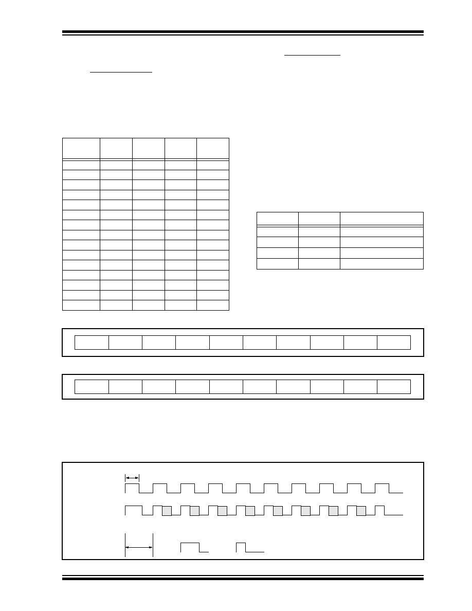
Serial Interface
The decoder has a PWM/Synchronous interface con-
nection to microcontrollers with limited I/O. An output
data stream is generated when a valid transmission is
received. The data stream consists of one start bit, four
function bits, one bit for battery status, one bit to indi-
cate a repeated transmission, two status bits, and one
stop bit. (Table 3-1). The DATA and CLK lines are used
to send a synchronous event message.
A special status message is transmitted on the second
pass of learn. This allows the controlling microcontroller
to determine if the learn was successful (Result = 1)
and if a previous transmitter was overwritten (Overwrite
= 1). The status message is shown in Figure 3-2.
Table 3-2 show the values for TX1:0 and the number of
transmitters learned.
TABLE 3-2:
STATUS BITS
FIGURE 3-1:
DATA OUTPUT FORMAT
FIGURE 3-2:
STATUS MESSAGE FORMAT
A 1-wire PWM or 2-wire synchronous interface can be used.
In 1-wire mode, the data is transmitted as a PWM signal with a basic pulse width of 400
µ
s.
In 2-wire mode, synchronous mode PWM bits start on the rising edge of the clock, and the bits must be sampled on the
falling edge. The start and stop bits are `1'.
FIGURE 3-3:
PWM TRANSMISSION FORMAT
Function
Code
S3
S2
S1
S0
0001
0
0
0
1
0010
0
0
1
0
0011
0
0
1
1
0100
0
1
0
0
0101
0
1
0
1
0110
0
1
1
0
0111
0
1
1
1
1000
1
0
0
0
1001
1
0
0
1
1010
1
0
1
0
1011
1
0
1
1
1100
1
1
0
0
1101
1
1
0
1
1110
1
1
1
0
1111
1
1
1
1
TX1
TX0
Number of Transmitters
0
0
One
0
1
Two
1
0
Three
1
1
Four
START
S3
S2
S1
S0
V
LOW
TX1
TX0
STOP
REPEAT
START
0
0
0
0
RESULT
TX1
TX0
STOP
OVRWR
S3
Start
S2
S1
S0
V
LOW
RPT Reserved Reserved Stop
1200
µ
s
CLK
DATA
"1"
"0"
600
µ
s