 | –≠–ª–µ–∫—Ç—Ä–æ–Ω–Ω—ã–π –∫–æ–º–ø–æ–Ω–µ–Ω—Ç: HCS515 | –°–∫–∞—á–∞—Ç—å:  PDF PDF  ZIP ZIP |
©
1998 Microchip Technology Inc.
Preliminary
DS40183A-page 1
M
HCS515
FEATURES
Security
∑ Encrypted storage of manufacturer's code
∑ Encrypted storage of encoder decryption keys
∑ Up to seven transmitters can be learned
∑
K
EE
L
OQ
code hopping technology
∑ Normal and secure learning mechanisms
Operating
∑ 3.0V--5.5V operation
∑ Internal oscillator
∑ Auto bit rate detection
Other
∑ Stand-alone decoder
∑ Internal EEPROM for transmitter storage
∑ Synchronous serial interface
∑ 1 Kbit user EEPROM
∑ 14-pin DIP/SOIC package
Typical Applications
∑ Automotive remote entry systems
∑ Automotive alarm systems
∑ Automotive immobilizers
∑ Gate and garage openers
∑ Electronic door locks
∑ Identity tokens
∑ Burglar alarm systems
Compatible Encoders
∑ HCS200, HCS300, HCS301, HCS360, HCS361,
HCS410 (PWM Mode)
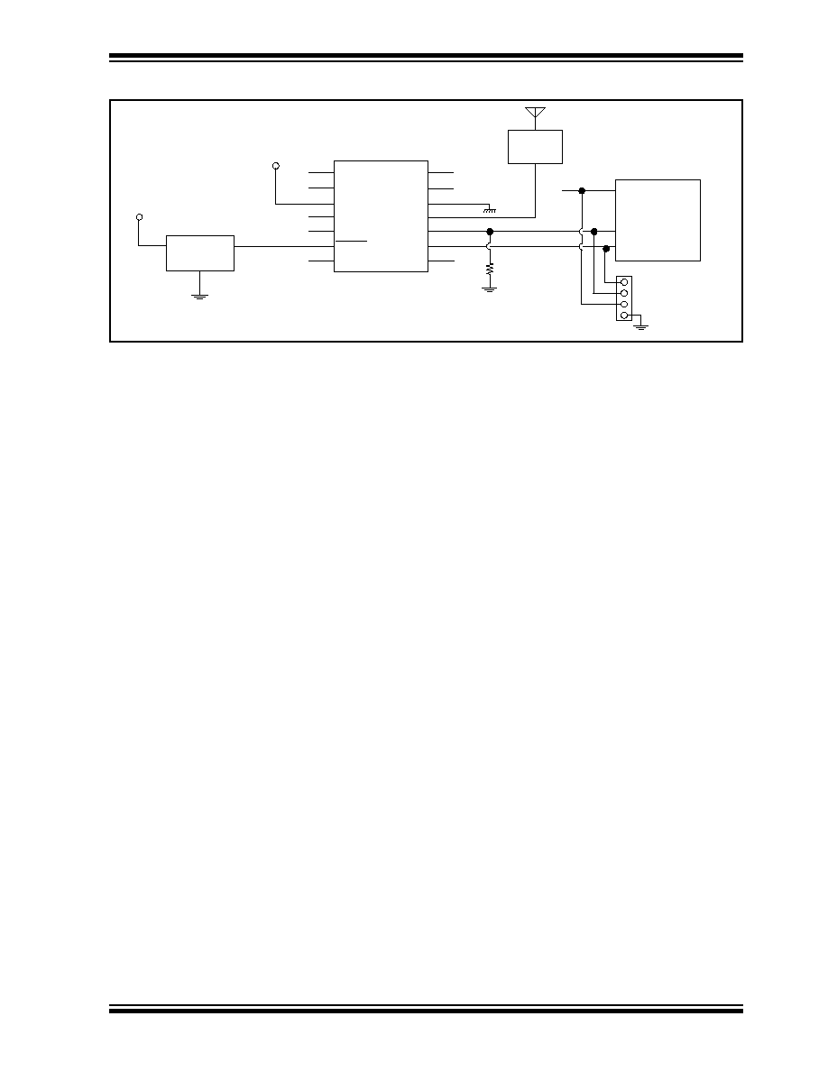
DESCRIPTION
The Microchip Technology Inc. HCS515 is a code hop-
ping decoder designed for secure Remote Keyless
Entry (RKE) systems. The HCS515 utilizes the pat-
ented K
EE
L
OQ
code hopping system and high security
learning mechanisms to make this a canned solution
when used with the HCS encoders to implement a uni-
directional remote and access control systems. The
HCS515 can be used as a stand-alone decoder or in
conjunction with a microcontroller.
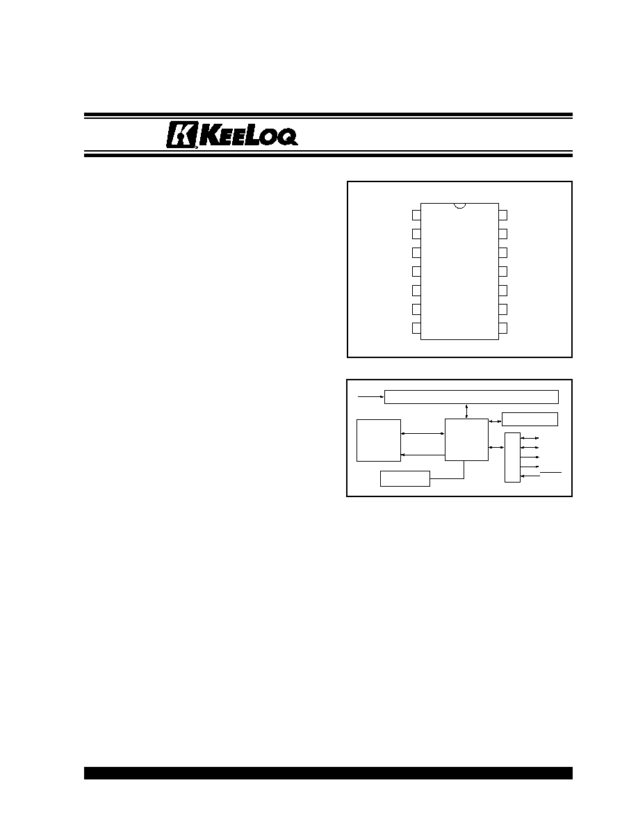
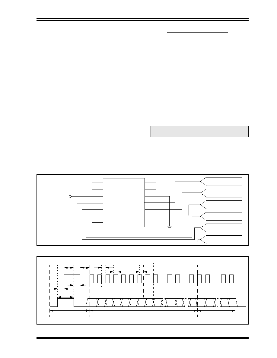
PACKAGE TYPE
BLOCK DIAGRAM
The manufacturer's code, encoder decryption keys,
and synchronization information are stored in
encrypted form in internal EEPROM. The HCS515
uses the S_DAT and S_CLK inputs to communicate
with a host controller device.
The HCS515 operates over a wide voltage range of
3.0 volts to 5.5 volts. The decoder employs automatic
bit-rate detection, which allows it to compensate for
wide variations in transmitter data rate. The decoder
contains sophisticated error checking algorithms to
ensure only valid codes are accepted.
HCS515
PDIP, SOIC
1
2
3
4
NC
NC
Vdd
S0
NC
NC
Vss
RF_IN
5
6
7
14
13
12
11
10
9
8
S1
MCLR
NC
S_CLK
S_DAT
NC
67-bit Reception Register
Internal
CONTROL
DECRYPTOR
RFIN
OSCILLATOR
S_DAT
S_CLK
MCLR
EEPROM
EE_DAT
EE_CLK
S0
S1
Code Hopping Decoder
The K
EE
L
OQ
name, K
EE
L
OQ
logo, and logotype are registered trademarks of Microchip Technology Inc. in the U.S.A. and other countries.
*Code hopping patents issued in Europe, U. S. A. and R. S.--US:5,517,187; Europe: 0459781
HCS515
DS40183A-page 2
Preliminary
©
1998 Microchip Technology Inc.
1.0
K
EE
L
OQ
SYSTEM OVERVIEW
1.1
Key Terms
∑ Manufacturer's Code ≠ A 64-bit word, unique to
each manufacturer, used to produce a unique
encoder decryption key in each transmitter.
∑ Encoder Decryption Key ≠ A 64-bit key, unique for
each transmitter. The encoder decryption key
controls the K
EE
L
OQ
decryption algorithm and is
stored in EEPROM on the decoder device.
∑ Learn ≠ The receiver uses information that is
transmitted to derive the transmitter's encoder
decryption key, decrypt the discrimination value,
and the synchronization counter in learning mode.
The encoder decryption key is a function of the
manufacturer's code and the device serial number
and/or seed value.
The HCS encoders and decoders employ the K
EE
L
OQ
code hopping technology and a K
EE
L
OQ
encryption
algorithm to achieve a high level of security. Code
hopping is a method by which the code transmitted
from the transmitter to the receiver is different every
time a button is pushed. This method, coupled with a
transmission length of 66 bits, virtually eliminates the
use of code `grabbing' or code `scanning'.
1.2
HCS Encoder Overview
The HCS encoders have a small EEPROM array which
must be loaded with several parameters before use.
The most important of these values are:
∑ An encoder decryption key that is generated at
the time of production
∑ A 16-bit synchronization counter value
∑ A 28-bit serial number which is meant to be
unique for every encoder
The manufacturer programs the serial number for each
encoder at the time of production, while the `Key Gen-
eration Algorithm' generates the encoder decryption
key (Figure 1-1). Inputs to the key generation algorithm
typically consist of the encoder's serial number and a
64-bit manufacturer's code, which the manufacturer
creates.
The 16-bit synchronization counter is the basis for the
transmitted code changing for each transmission and is
updated each time a button is pressed. Because of the
complexity of the K
EE
L
OQ
encryption algorithm, a
change in one bit of the synchronization counter value
will result in a large change in the actual transmitted
code. There is a relationship (Figure 1-2) between the
encoder decryption key values in EEPROM and how
they are used in the encoder. Once the encoder
detects that a button has been pressed, the encoder
reads the button and updates the synchronization
counter. The synchronization value is then combined
with the encoder decryption key in the K
EE
L
OQ
encryption algorithm, and the output is 32 bits of
encrypted information. This data will change with every
button press, hence, it is referred to as the code hop-
ping portion of the code word. The 32-bit code hopping
portion is combined with the button information and the
serial number to form the code word transmitted to the
receiver.
FIGURE 1-1:
CREATION AND STORAGE OF ENCRYPTION KEY DURING PRODUCTION
Note:
The manufacturer code is a pivotal part of
the system's overall security. Conse-
quently, all possible precautions must be
taken and maintained for this code.
Transmitter
Manufacturer's
Serial Number or
Code
Encryption
Key
Key
Generation
Algorithm
Serial Number
Encryption Key
Sync Counter
.
.
.
HCS515 EEPROM Array
Seed

HCS515
©
1998 Microchip Technology Inc.
Preliminary
DS40183A-page 3
1.3
HCS Decoder Overview
Before a transmitter and receiver can work together,
the receiver must first `learn' and store certain informa-
tion from the transmitter. This information includes a
`check value' of the serial number, the encoder decryp-
tion key, and current synchronization counter value.
When a valid formatted message is detected, the
receiver first compares the serial number. If the serial
number check value is from a learned transmitter, the
message is decrypted. Next, the receiver checks the
decrypted synchronization counter value against what
is stored in memory. If the synchronization counter
value is verified, then a valid transmission message is
sent. Figure 1-3 shows the relationship between some
of the values stored by the receiver and the values
received from the transmitter.
FIGURE 1-2:
BASIC OPERATION OF A CODE HOPPING TRANSMITTER (ENCODER)
FIGURE 1-3:
BASIC OPERATION OF A CODE HOPPING RECEIVER (DECODER)
K
EE
L
OQ
Algorithm
Button Press
Information
Encryption
EEPROM Array
32 Bits of
Encrypted Data
Serial Number
Transmitted Information
Encoder Decryption Key
Sync. Counter Value
Serial Number
Button Press
Information
EEPROM Array
Encoder Decryption Key
32 Bits of
Encrypted Data
Serial Number
Received Information
Decrypted
Synchronization
Counter
Check for
Match
Check for
Match
K
EE
L
OQ
Algorithm
Decryption
Sync. Counter Value
Serial Number
Manufacturer Code

HCS515
DS40183A-page 4
Preliminary
©
1998 Microchip Technology Inc.
2.0
PIN ASSIGNMENT
PIN
Decoder
Function
I/O
(1)
Buffer
Type
(1)
Description
1
NC
--
--
No connection
2
NC
--
--
No connection
3
V
DD
--
--
Power connection
4
S0
O
TTL
S0 function output
5
S1
O
TTL
S1 function output
6
MCLR
I
ST
Master clear input
7
NC
--
--
No connection
8
NC
--
--
No connection
9
S_DAT
I/O
TTL
Synchronous data from controller
10
S_CLK
I
TTL
Synchronous clock from controller
11
RF_IN
I
TTL
RF input from receiver
12
GND
--
--
Ground connection
13
NC
--
--
No connection
14
NC
--
--
No connection
Note:
P = power, I = in, O = out, and ST = Schmitt Trigger input.
HCS515
©
1998 Microchip Technology Inc.
Preliminary
DS40183A-page 5
3.0
DECODER OPERATION
3.1
Learning a Transmitter to a Receiver
(Normal or Secure Learn)
Before the transmitter and receiver can work together,
the receiver must first `learn' and store the following
information from the transmitter in EEPROM:
∑ A check value of the serial number
∑ The encoder decryption key
∑ The current synchronization counter value
The decoder must also store the manufacturer's code
(Section 1.2) in protected memory. This code will
typically be the same for all of the decoders in a sys-
tem.
The HCS515 has seven memory slots, and, conse-
quently, can store up to seven transmitters. During the
learn procedure, the decoder searches for an empty
memory slot for storing the transmitter's information.
When all of the memory slots are full, the decoder will
overwrite the last transmitter's information. To erase all
of the memory slots at once, use the ERASE_ALL
command (C3H).
3.1.1
LEARNING PROCEDURE
Learning is initiated by sending the ACTIVATE_LEARN
(D2H) command to the decoder. The decoder acknowl-
edges reception of the command by pulling the data
line high.
For the HCS515 decoder to learn a new transmitter, the
following sequence is required:
1.
Activate the transmitter once.
2.
Activate the transmitter a second time. (In
secure learning mode, the seed transmission
must be transmitted during the second stage of
learn by activating the appropriate buttons on
the transmitter.)
The HCS515 will transmit a learn-status string,
indicating that the learn was successful.
3.
The decoder has now learned the transmitter.
4.
Repeat steps 1-3 to learn up to seven
transmitters
Note 1:
Learning will be terminated if two
nonsequential codes were received or if two
acceptable codes were not decoded within
30 seconds.
2:
If more than seven transmitters are learned,
the new transmitter will replace the last
transmitter learned. It is, therefore, not pos-
sible to erase lost transmitters by
repeatedly learning new transmitters. To
remove lost or stolen transmitters,
ERASE_ALL transmitters and relearn all
available transmitters.
3:
Learning a transmitter with an encoder
decryption key that is identical to a transmit-
ter already in memory replaces the existing
transmitter. In practice, this means that all
transmitters should have unique encoder
decryption keys. Learning a previously
learned transmitter does not use any addi-
tional memory slots.
The following checks are performed by the decoder to
determine if the transmission is valid during learn:
∑ The first code word is checked for bit integrity.
∑ The second code word is checked for bit integrity.
∑ The encoder decryption key is generated accord-
ing to the selected algorithm.
∑ The hopping code is decrypted.
∑ The discrimination value is checked.
∑ If all the checks pass, the key, serial number
check value, and synchronization counter values
are stored in EEPROM memory.
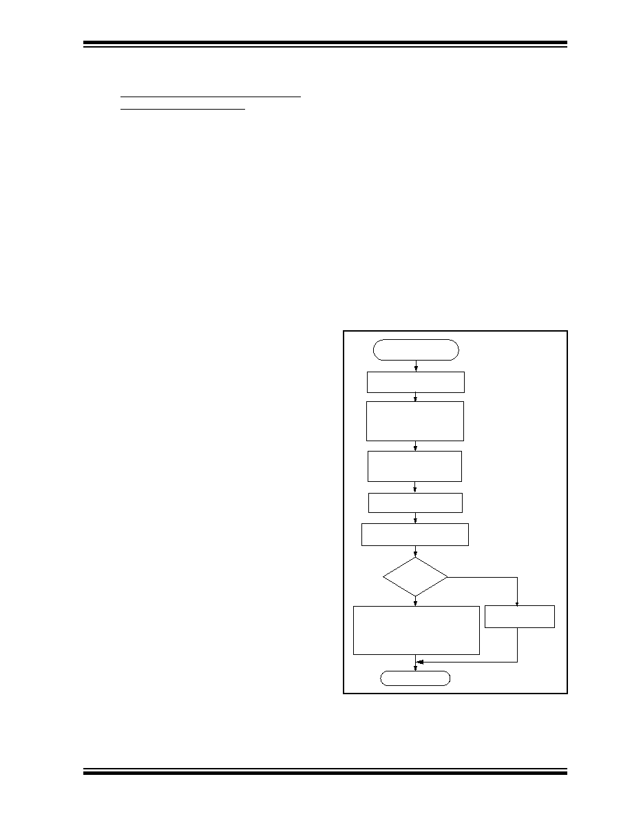
Figure 3-1 shows a flow chart of the learn sequence.
FIGURE 3-1:
LEARN SEQUENCE
Enter Learn
Mode
Wait for Reception
of Second
Compare Discrimination
Value with Serial Number
Use Generated Key
to Decrypt
Equal?
Sync. counter value
Encoder decryption key
Exit
Learn successful. Store:
Learn
Unsuccessful
No
Yes
Wait for Reception
of a Valid Code
Non-Repeated
Valid Code
Generate Key
from Serial Number/
Seed Value
Serial number check value
HCS515
DS40183A-page 6
Preliminary
©
1998 Microchip Technology Inc.
3.2
Validation of Codes
The decoder waits for a transmission and checks the
serial number to determine if it is a learned transmitter.
If it is, it takes the code hopping portion of the transmis-
sion and decrypts it, using the encoder decryption key.
It uses the discrimination value to determine if the
decryption was valid. If everything up to this point is
valid, the synchronization counter value is evaluated.
3.3
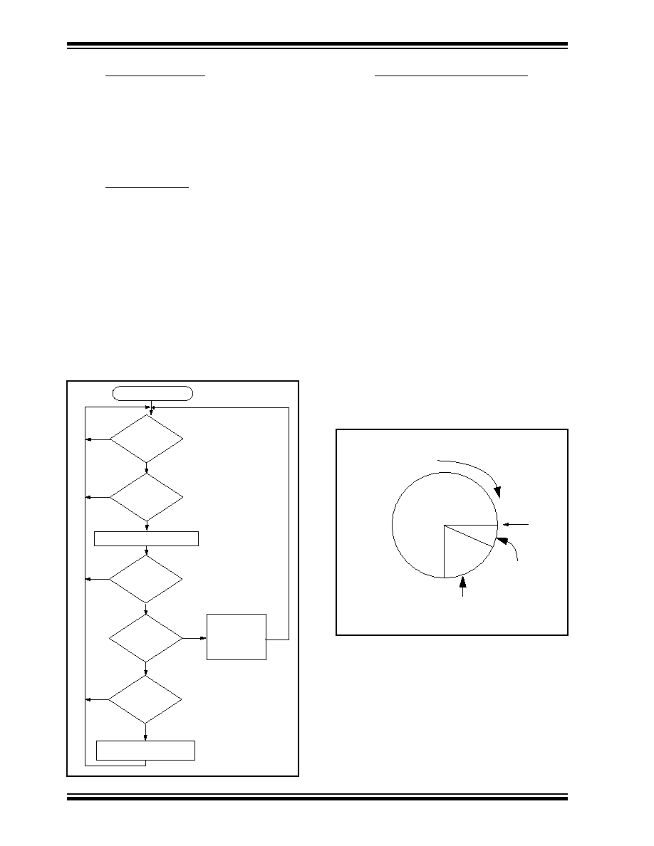
Validation Steps
Validation consists of the following steps:
1.
Search EEPROM to find the Serial Number
Check Value Match
2.
Decrypt the Hopping Code
3.
Compare the 10 bits of the discrimination value
with the lower 10 bits of serial number
4.
Check if the synchronization counter value falls
within the first synchronization window.
5.
Check if the synchronization counter value falls
within the second synchronization window.
6.
If a valid transmission is found, update the
synchronization counter, else use the next
transmitter block, and repeat the tests.
FIGURE 3-2:
DECODER OPERATION
3.4
Synchronization with Decoder
The K
EE
L
OQ
technology features a sophisticated
synchronization technique (Figure 3-3) which does not
require the calculation and storage of future codes. If
the stored synchronization counter value for that
particular transmitter and the synchronization counter
value that was just decrypted are within a formatted
window of 16, the counter is stored, and the command
is executed. If the synchronization counter value was
not within the single operation window, but is within the
double operation window of the 16K window, the
transmitted synchronization counter value is stored in a
temporary location, and the decoder goes back to wait-
ing for another transmission. When the next valid
transmission is received, it will check the new
synchronization counter value with the one in tempo-
rary storage. If the two values are sequential, it is
assumed that the counter had just gotten out of the
single operation `window', but is now back in synchroni-
zation, so the new synchronization counter value is
stored, and the command is executed. If a transmitter
has somehow gotten out of the double operation
window, the transmitter will not work and must be
relearned. Since the entire window rotates after each
valid transmission, codes that have been used become
part of the `blocked' (48K) codes and are no longer
valid. This eliminates the possibility of grabbing a previ-
ous code and retransmitting to gain entry.
FIGURE 3-3:
SYNCHRONIZATION WINDOW
Transmission
Received?
Does
Ser # Check Val
Match?
Decrypt Transmission
Is
decryption
valid?
Is
counter within
16?
Is
counter within
16K?
Update
Counter
Execute
Command
Save Counter
in Temp Location
Start
No
No
No
No
Yes
Yes
Yes
Yes
Yes
No
and
Blocked
Entire Window
rotates to eliminate
use of previously
used codes
Current
Position
(48K Codes)
Double
Operation
(16K Codes)
Single
Operation
Window
(16 Codes)
HCS515
©
1998 Microchip Technology Inc.
Preliminary
DS40183A-page 7
4.0
INTERFACING TO A
MICROCONTROLLER
The HCS515 interfaces to a microcontroller via a syn-
chronous serial interface. A clock and data line are
used to communicate with the HCS515. The microcon-
troller controls the clock line. There are two groups of
data transfer messages. The first is from the decoder
whenever the decoder receives a valid transmission.
The decoder signals reception of a valid code by taking
the data line high (maximum of 500 ms) The microcon-
troller then services the request by clocking out a data
string from the decoder. The data string contains the
function code, the status bit, and block indicators. The
second is from the controlling microcontroller to the
decoder in the form of a defined command set.
Figure 4-1 shows the HCS515 decoder and the I/O
interface lines necessary to interface to a microcontrol-
ler.
4.1
Valid Transmission Message
The decoder informs the microcontroller of a valid
transmission by taking the data line high for up to
500 ms. The controlling microcontroller must acknowl-
edge by taking the clock line high. The decoder then
takes the data line low. The microcontroller can then
begin clocking a data stream out of the HCS515. The
data stream consists of:
∑ Start bit `0'.
∑ 2 status bits [REPEAT, VLOW].
∑ 4-bit function code [S3 S2 S1 S0].
∑ Stop bit `1'.
∑ 4 bits indicating the number of transmitters
learned into the decoder [CNT3...CNT0].
∑ 4 bits indicating which block was used
[TX3...TX0].
∑ 64 bits of the received transmission with the hop-
ping code decrypted.
The decoder will terminate the transmission of the data
stream at any point where the clock is kept low for
longer than 1 ms.Therefore, the microcontroller can
only clock out the required bits. A maximum of 80 bits
can be clocked out of the decoder.
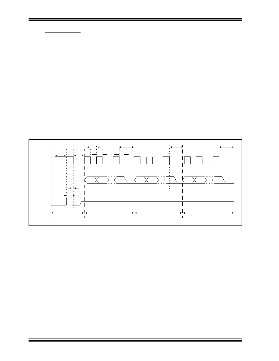
FIGURE 4-1:
HCS515 DECODER AND I/O INTERFACE LINES
FIGURE 4-2:
DECODER VALID TRANSMISSION MESSAGE
Note:
Data is always clocked in/out Least
Significant Bit (LSB) first.
NC
NC
V
DD
S0
RF DATA
SYNC CLOCK
SYNC DATA
S1 OUTPUT
HCS515
S1
MCLR
NC
NC
NC
V
SS
RF_IN
S_CLK
S_DAT
NC
1
2
3
4
5
6
7
8
9
10
11
12
13
14
V
CC
X
X
X
MICRO RESET
S0 OUTPUT
X
X
X
Decoder Signal Valid
T
CLKH
T
DS
A
B
Cii
T
ACT
T
DHI
T
CLA
Received String
Ci
S_DAT
TX0
TX3
RX63
REPT V
LOW
S0
S1
S2
S3
CNT0
CNT3
0
RX0
RX1
RX62
1
S_CLK
Information
T
ACK
T
CLKH
T
CLKL
Transmission
HCS515
DS40183A-page 8
Preliminary
©
1998 Microchip Technology Inc.
4.2
Command Mode
4.2.1
MICROCONTROLLER COMMAND MODE
ACTIVATION
The microcontroller command consists of four parts.
The first part activates the command mode, the second
part is the actual command, the third is the address
accessed, and the last part is the data. The microcon-
troller starts the command by taking the clock line high
for up to 500 ms. The decoder acknowledges the start-
up sequence by taking the data line high. The micro-
controller takes the clock line low, after which the
decoder will take the data line low, tri-state the data line
and wait for the command to be clock in. The data must
be set up on the rising edge and will be sampled on the
falling edge of the clock line.
4.2.2
COLLISION DETECTION
The HCS515 uses collision detection to prevent
clashes between the decoder and microcontroller.
Whenever the decoder receives a valid transmission
the following sequence is followed:
∑ The decoder first checks to see if the clock line is
high. If the clock line is high, the valid transmis-
sion notification is aborted, and the microcontrol-
ler command mode request is serviced.
∑ The decoder takes the data line high and checks
that the clock line doesn't go high within 50
µ
s. If
the clock line goes high, the valid transmission
notification is aborted and the command mode
request is serviced.
∑ If the clock line goes high after 50
µ
s but before
500 ms, the decoder will acknowledge by taking
the data line low.
∑ The microcontroller can then start to clock out the
80-bit data stream of the received transmission.
FIGURE 4-3:
MICROCONTROLLER COMMAND MODE ACTIVATION
MSB
A
Command Byte
Start Command
T
CLKL
T
CLKH
T
DS
B
C
LSB
T
START
T
CMD
D
T
DATA
E
Address Byte
Data Byte
T
ADDR
T
REQ
T
RESP
CLK
µ
C Data
HCS515
Data
MSB
LSB
MSB
LSB
T
ACK

HCS515
©
1998 Microchip Technology Inc.
Preliminary
DS40183A-page 9
4.2.3
COMMAND ACTIVATION TIMES
The command activation time (Table 4-1) is defined as
the maximum time the microcontroller has to wait for a
response from the decoder. The decoder will abort and
service the command request. The response time
depends on the state of the decoder when the com-
mand mode is requested.
4.2.4
DECODER COMMANDS
The command byte specifies the operation required by
the controlling microcontroller. Table 4-2 lists the com-
mands.
TABLE 4-1:
COMMAND ACTIVATION TIMES
Decoder State
Min
Max
While receiving transmissions
--
2 1/2 BPW
MAX
= 2.7 ms
During the validation of a received transmission
--
3 ms
During the update of the sync counters
--
40 ms
During learn
--
170 ms
TABLE 4-2:
DECODER COMMANDS
Instruction
Command Byte
Operation
READ
F0
16
Read a byte from user EEPROM
WRITE
E1
16
Write a byte to user EEPROM
ACTIVATE_LRN
D2
16
Activate a learn sequence on the decoder
ERASE_ALL
C3
16
Activate an erase all function on the decoder
PROGRAM
B4
16
Program manufacturer's code and configuration byte
HCS515
DS40183A-page 10
Preliminary
©
1998 Microchip Technology Inc.
4.2.5
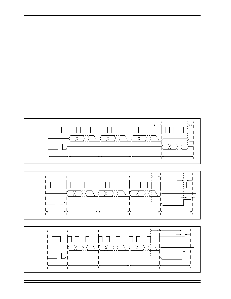
READ BYTE/S FROM USER EEPROM
The read command (Figure 4-4) is used to read bytes
from the user EEPROM. The offset in the user
EEPROM is specified by the address byte which is
truncated to seven bits (C to D). After the address, a
dummy byte must be clocked in (D to E). The EEPROM
data byte is clocked out on the next rising edge of the
clock line with the least significant bit first (E to F).
Sequential reads are possible by repeating sequence E
to F within 1 ms after the falling edge of the previous
byte's Most Significant Bit (MSB) bit. During the
sequential read, the address value will wrap after 128
bytes. The decoder will terminate the read command if
no clock pulses are received for a period longer than
1.2 ms.
4.2.6
WRITE BYTE/S TO USER EEPROM
The write command (Figure 4-5) is used to write a loca-
tion in the user EEPROM. The address byte is trun-
cated to seven bits (C to D). The data is clocked in least
significant bit first. The clock line must be asserted to
initiate the write. Sequential writes of bytes are possible
by clocking in the byte and then asserting the clock line
(D ≠ F). The decoder will terminate the write command
if no clock pulses are received for a period longer than
1.2 ms After a successful write sequence the decoder
will acknowledge by taking the data line high and keep-
ing it high until the clock line goes low.
4.2.7
ERASE ALL
The erase all command (Figure 4-6) erases all the
transmitters in the decoder. After the command and two
dummy bytes are clocked in, the clock line must be
asserted to activate the command. After a successful
completion of an erase all command, the data line is
asserted until the clock line goes low.
FIGURE 4-4:
READ BYTES FROM USER EEPROM
FIGURE 4-5:
WRITE BYTES TO USER EEPROM
FIGURE 4-6:
ERASE ALL
Decoder DATA
MSB
A
Command Byte
Start Command
B
C
LSB
D
T
RD
E
Address Byte
Dummy Byte
CLK
µ
C DATA
F
Data Byte
MSB
LSB
MSB
LSB
MSB
LSB
T
RD
Decoder DATA
MSB
A
Command Byte
Start Command
B
C
LSB
D
T
WR
E
Address Byte
Data Byte
CLK
µ
C DATA
F
Acknowledge
MSB
LSB
MSB
LSB
T
ACK
T
RESP
T
ACK
2
Decoder DATA
MSB
A
Command Byte
Start Command
B
C
LSB
D
T
ERA
E
Subcommand Byte
Dummy Byte
CLK
µ
C DATA
F
Acknowledge
MSB
LSB
MSB
LSB
T
ACK
T
RESP
T
ACK
2
HCS515
©
1998 Microchip Technology Inc.
Preliminary
DS40183A-page 11
4.2.8
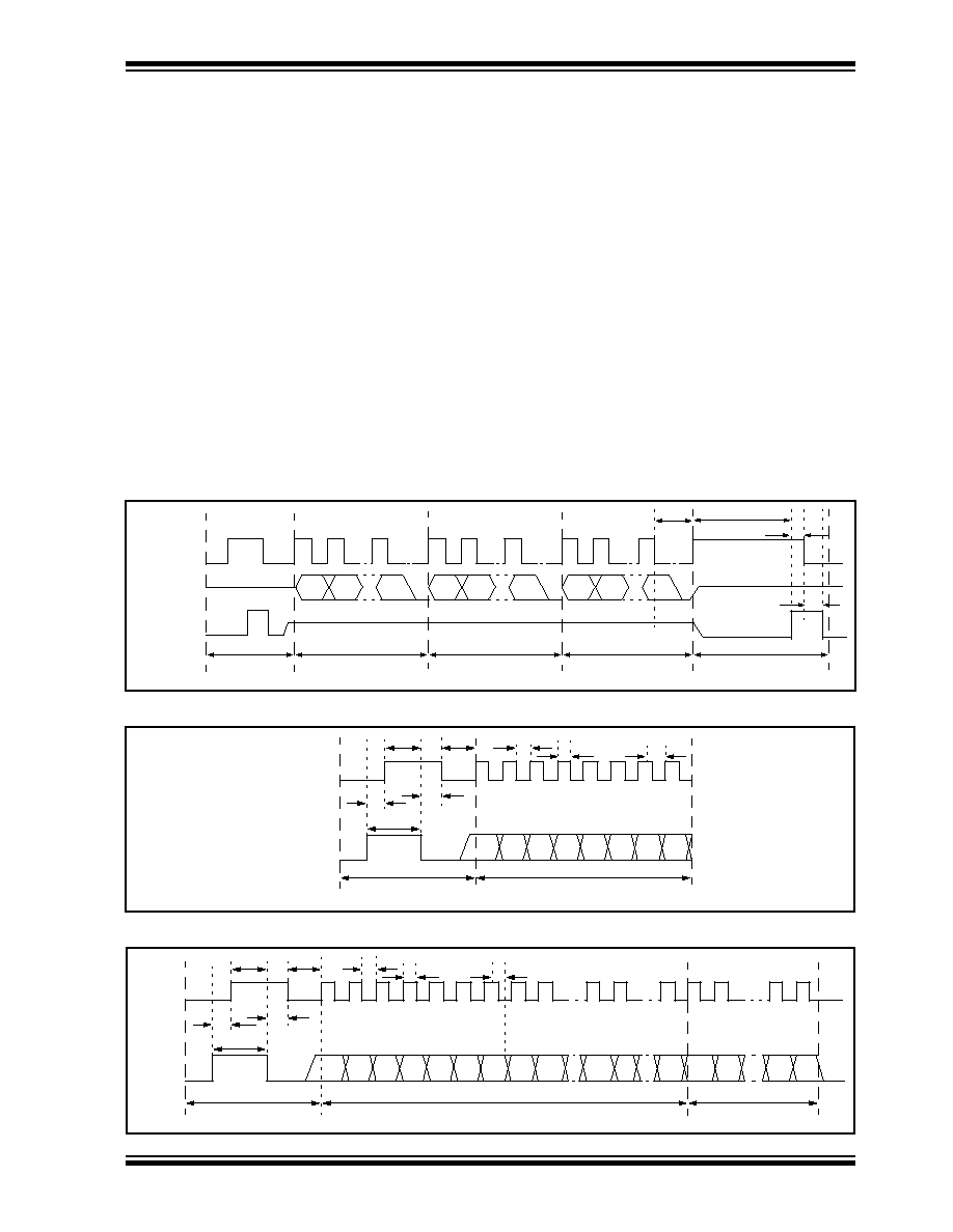
ACTIVATE LEARN
The activate learn command (Figure 4-7) is used to
activate a transmitter learning sequence on the
decoder. The command consists of a command mode
activation sequence, a command byte, and two dummy
bytes. The decoder will respond by taking the data line
high to acknowledge that the command was valid and
that learn is active.
Upon reception of the first transmission, the decoder
will respond with a learn status message (Figure 4-8).
During learn, the decoder will acknowledge the recep-
tion of the first transmission by taking the data line high
for 60 ms. The controlling microcontroller can clock out
at most eight bits, which will all be zeros. All of the bits
of the status byte are zero, and this is used to distin-
guish between a learn time-out status string and the
first transmission received string. The controlling micro-
controller must ensure that the clock line does not go
high 60 ms after the falling edge of the data line, for this
will terminate learn.
Upon reception of the second transmission, the
decoder will respond with a learn status message
(Figure 4-9).
The learn status message after the second transmis-
sion consists of the following:
∑ 1 start bit.
∑ The function code [S3:S0] of the message is zero,
indicating that this is a status string.
∑ The RESULT bit indicates the result of the learn
sequence. The RESULT bit is set if successful
and cleared otherwise.
∑ The OVR bit will indicate whether an exiting trans-
mitter is over written. The OVR bit will be set if an
existing transmitter is learned over.
∑ The [CNT3...CNT0] bits will indicate the number
of transmitters learned on the decoder.
∑ The [TX3...TX0] bits indicate the block number
used during the learning of the transmitter.
FIGURE 4-7:
LEARN MODE ACTIVATION
FIGURE 4-8:
LEARN STATUS MESSAGE AFTER FIRST TRANSMISSION
FIGURE 4-9:
LEARN STATUS MESSAGE AFTER SECOND TRANSMISSION
Decoder DATA
MSB
A
Command Byte
Start Command
B
C
LSB
D
T
LRN
E
Dummy Byte
Dummy Byte
CLK
µ
C DATA
F
Acknowledge
MSB
LSB
MSB
LSB
T
ACK
T
RESP
T
ACK
2
Command Request
T
CLKL
T
CLKH
T
CA
T
DS
A
B
T
CLL
T
DHI
T
CLA
T
CLH
CLK
Decoder
0
0
0
0
0
0
0
0
Status Byte
C
Data
Communications Request
T
CLKL
T
CLKH
T
ACT
T
DS
A
B
Cii
T
CLL
T
DHI
T
CLA
T
CLH
CLK
Decoder
TX0
TX3
RX63
OVR RSLT
0
0
0
0
CNT0
CNT3
0
RX0
RX1
RX62
1
Ci
Learn Status Bits
Decoded Tx
Data
HCS515
DS40183A-page 12
Preliminary
©
1998 Microchip Technology Inc.
4.3
Stand-alone Mode
The HCS515 decoder can also be used in stand-alone
applications. The HCS515 will activate the data line for
up to 500 ms if a valid transmission was received, and
this output can be used to drive a relay circuit. To acti-
vate learn or erase all commands, a button must be
connected to the CLK input. User feedback is indicated
on an LED connected to the DATA output line. If the
CLK line is pulled high, using the learn button, the LED
will switch on. After the CLK line is kept high for longer
than 2 seconds, the decoder will switch the LED line off,
indicating that learn will be entered if the button is
released. If the CLK line is kept high for another 6 sec-
onds, the decoder will activate an ERASE_ALL Com-
mand.
Learn mode can be aborted by taking the clock line
high until the data line goes high (LED switches on).
During learn, the data line will give feedback to the user
and, therefore, must not be connected to the relay drive
circuitry.
After taking the clock low and before a transmitter is
learn, any low-to-high change on the clock line may ter-
minate learn. This has learn implications when a switch
with contact bounce is used.
4.4
Erase All Command and Erase
Command
The Table 4-3 describes two versions of the Erase All
command.
Subcommand 01 can be used where a transmitter with
permanent status is implemented in the microcontroller
software. Use of subcommand 01 ensures that the per-
manent transmitter remains in memory even when all
other transmitters are erased. The first transmitter
learned after any of the following events is the first
transmitter in memory and becomes the permanent
transmitter:
1.
Programming of the manufacturer's code.
2.
Erasing of all transmitters
(subcommand 00 only).
4.5
Test Mode
A special test mode is activated after:
1.
Programming of the manufacturer's code.
2.
Erasing of all transmitters.
Test mode can be used to test a decoder before any
transmitters are learned on it. Test mode enables test-
ing of decoders without spending the time to learn a
transmitter. Test mode is terminated after the first suc-
cessful learning of an ordinary transmitter. In test
mode, the decoder responds to a test transmitter. The
test transmitter has the following properties:
1.
Encoder decryption key = manufacturer's code.
2.
Serial number = any value.
3.
Discrimination bits = lower 10 bits of the serial
number.
4.
Synchronization counter value = any value
(synchronization information is ignored).
Because the synchronization counter value is ignored
in test mode, any number of test transmitters can be
used, even if their synchronization counter values are
different.
Note:
The REPS bit must be cleared in the con-
figuration byte in stand-alone mode.
TABLE 4-3:
ERASE ALL COMMAND
Command
Byte
Subcommand
Byte
Description
C3
16
00
16
Erase all
transmitters.
C3
16
01
16
Erase all transmit-
ters except 1. The
first transmitter in
memory is not
erased.
HCS515
©
1998 Microchip Technology Inc.
Preliminary
DS40183A-page 13
4.6
Power Supply Supervisor
Reliable operation of the HCS515 requires that the
contents of the EEPROM memory be protected against
erroneous writes. To ensure that erroneous writes do
not occur after supply voltage "brown-out" conditions,
the use of a proper power supply supervisor device is
imperative (Figure 4-11 and Figure 8-4).
FIGURE 4-10: STAND-ALONE MODE LEARN/ERASE-ALL TIMING
FIGURE 4-11: TYPICAL STAND-ALONE APPLICATION CIRCUIT
DATA
A
Erase-All Activation
T
REQ
T
LRN
CLK
B
C
D
Learn Activation
T
ERA
Successful
E
T
LRN
OUTPUT
K2
RELAY SPST
Vcc
Vcc
S1
LEARN
Q2
NPN
10K
D1
LED
R2
10K
Vcc
VI
G
N
D
VO
U3
Brown-out Circuit
NC
NC
V
DD
S0
HCS515
S1
MCLR
NC
NC
NC
V
SS
RF_IN
S_CLK
S_DAT
NC
1
2
3
4
5
6
7
8
9
10
11
12
13
14
X
X
X
X
X
X
R3
10K
X
Vcc
R1
10K
ANT1
RF Circuit

HCS515
DS40183A-page 14
Preliminary
©
1998 Microchip Technology Inc.
5.0
DECODER PROGRAMMING
The memory is divided between system memory that stores the transmitter information (read protected) and user mem-
ory (read/write). Commands to access the user memory are described in Sections 4.2.5 and 4.2.6.
The following information stored in system memory needs to be programmed before the decoder can be used:
∑ 64-bit manufacturer's code
∑ Decoder configuration byte
5.1
Configuration Byte
The decoder is configured during initialization by setting the appropriate bits in the configuration byte. The following table
list the options:
5.1.1
LRN_MODE
LRN_MODE selects between two learning modes. With LRN_MODE = 0, the normal (serial number derived) mode is
selected; with LRN_MODE=1, the secure (seed derived) mode is selected. See Section 6.0 for more detail on learning
modes.
5.1.2
REPEAT
The HCS515 can be configured to indicate repeated transmissions. In a stand-alone configuration, repeated transmis-
sions must be disabled.
Note 1: These memory locations are read protected and can only be written to using the program command with
the device powered up.
2: The contents of the system memory is encrypted by a unique 64-bit key that is stored in the HCS515. To
initialize the system memory, the HCS515's program command must be used.
Bit
Mnemonic
Description
0
LRN_MODE
Learning mode selection
LRN_MODE = 0--Normal Learn
LRN_MODE = 1--Secure Learn
1
Not Used
Reserved
2
REPEAT
Repeat Transmission enable
0 = Disable
1 = Enabled
3
Not Used
Reserved
4
Not Used
Reserved
5
Not Used
Reserved
6
Not Used
Reserved
7
Not Used
Reserved
HCS515
©
1998 Microchip Technology Inc.
Preliminary
DS40183A-page 15
5.2
Programming Waveform
The programming command consists of the following:
∑ Command Request Sequence (A to B)
∑ Command Byte (B to C)
∑ Configuration Byte (C to D)
∑ Manufacturer's Code Eight Data Bytes (D to G)
∑ Activation and Acknowledge Sequence (G to H)
5.3
Programming Data String
A total of 80 bits are clocked into the decoder. The 8-bit
command byte is clocked in first, followed by the 8-bit
configuration byte and the 64-bit manufacturer's code.
The data must be clocked in Least Significant Bit (LSB)
first. The decoder will then encrypt the manufacturer's
code using the decoder's unique 64-bit EEPROM
encoder decryption key. After completion of the pro-
gramming EEPROM, the decoder will acknowledge by
taking the data line high (G to H). If the data line goes
high within 30 ms after the clock goes high, program-
ming also fails.
FIGURE 5-1:
PROGRAMMING WAVEFORM
DECODER DATA
MSB
MSB
A
Command Byte
Start Command
T
CLKL
T
CLKH
T
PP
1
T
DS
B
C
LSB
T
PP
3
T
PP
2
T
CMD
D
LSB
LSB
Configuration Byte
CLK
µ
C DATA
MSB
T
DATA
G
Most Significant Byte
H
T
ACK
T
WT
2
T
AW
Acknowledge
MSB
E
Least Significant Byte
F
T
DATA
T
ADDR
T
PP
4

HCS515
DS40183A-page 16
Preliminary
©
1998 Microchip Technology Inc.
6.0
KEY GENERATION
The HCS515 supports two learning schemes which are selected during the initialization of the system EEPROM. The
learning schemes are:
∑ Normal learn using the K
EE
L
OQ
decryption algorithm
∑ Secure learn using the K
EE
L
OQ
decryption algorithm
6.1
Normal (Serial Number derived) Learn using the K
EE
L
OQ
Decryption Algorithm
This learning scheme uses the K
EE
L
OQ
decryption algorithm and the 28-bit serial number of the transmitter to derive
the encoder decryption key. The 28-bit serial number is patched with predefined values as indicated below to form two
32-bit seeds.
SourceH = 60000000 00000000H + Serial Number |
28 Bits
SourceL = 20000000 00000000H + Serial Number |
28 Bits
Then, using the K
EE
L
OQ
decryption algorithm and the manufacturer's code the encoder decryption key is
derived as follows:
KeyH
Upper 32 bits
= F
K
EE
L
OQ
Decryption
(SourceH) |
64-Bit Manufacturer's Code
KeyL
Lower 32 bits
= F
K
EE
L
OQ
Decryption
(SourceL) |
64-Bit Manufacturer's Code
6.2
Secure (Seed Derived) Learn using the K
EE
L
OQ
Decryption Algorithm
This scheme uses the secure seed transmitted by the encoder to derive the two input seeds. The decoder always uses
the lower 64 bits of the transmission to form a 60-bit seed. The upper 4 bits are always forced to zero.
For 32-bit seed encoders (HCS200/HCS300/HCS301):
SourceH = Serial Number
Lower 28 bits
SourceL = Seed
32 bits
For 48-bit seed encoders (HCS360/HCS361):
SourceH = Seed
Upper 16 bits
+ Serial Number
Upper 16 bits
with upper 4 bits set to zero
SourceL = Seed
Lower
32 bits
For 60-bit seed encoders (HCS410):
SourceH = Seed
Upper 32 bits
with upper 4 bits set to zero
SourceL = Seed
Lower 32 bits
The K
EE
L
OQ
decryption algorithm and the manufacturer's code is used to derive the encoder decryption key as
follows:
KeyH
Upper 32 bits
= F
K
EE
L
OQ
Decrypt
(SourceH) |
64 Bit Manufacturer's Code
KeyL
Lower 32 bits
= F
K
EE
L
OQ
Decrypt
(SourceL) |
64 Bit Manufacturer's Code

HCS515
©
1998 Microchip Technology Inc.
Preliminary
DS40183A-page 17
7.0
K
EE
L
OQ
ENCODERS
7.1
Transmission Format (PWM)
The K
EE
L
OQ
encoder transmission is made up of sev-
eral parts (Figure 7-1). Each transmission begins with
a preamble and a header, followed by the encrypted
and then the fixed data. The actual data is 66/67 bits
which consists of 32 bits of encrypted data and 34/35
bits of non-encrypted data. Each transmission is fol-
lowed by a guard period before another transmission
can begin. The code hopping portion provides up to
four billion changing code combinations and includes
the button status bits (based on which buttons were
activated), along with the synchronization counter
value and some discrimination bits. The non-code hop-
ping portion is comprised of the status bits, the function
bits, and the 28-bit serial number. The encrypted and
non-encrypted combined sections increase the num-
ber of combinations to 7.38 x 10
19
.
7.2
Code Word Organization
The HCS encoder transmits a 66/67-bit code word
when a button is pressed. The 66/67-bit word is con-
structed from a code hopping portion and a non-code
hopping portion (Figure 7-2).
The Encrypted Data is generated from four button bits,
two overflow counter bits, ten discrimination bits, and
the 16-bit synchronization counter value.
The Non-encrypted Data is made up from 2 status
bits, 4 function bits, and the 28/32-bit serial number.
FIGURE 7-1:
CODE WORD TRANSMISSION FORMAT
FIGURE 7-2:
CODE WORD ORGANIZATION
LOGIC `0'
LOGIC `1'
Bit
Period
Preamble
Header
Code Hopping Portion
of Transmission
Fixed Portion of
Transmission
Guard
Time
T
P
T
H
T
HOP
T
FIX
T
G
Repeat
V
LOW
(1 bit)
Button Status
S2S1S0S3
(4 bits)
28-bit
Serial
Number
Button Status
S2S1S0S3
(4 bits)
Discrimination
bits (12 bits)
16-bit
Sync.
Counter
Value
CRC1*
CRC0*
3/2 bits
+
Serial Number and
Button Status (32 bits)
+
32 bits of Encrypted Data
Encrypted Data
Non-encrypted Data
*HCS360/361
66/67 bits
of Data
Transmitted

HCS515
DS40183A-page 18
Preliminary
©
1998 Microchip Technology Inc.
8.0
ELECTRICAL CHARACTERISTICS FOR HCS515
Absolute Maximum Ratings
Ambient temperature under bias .............................................................................................................. -40
∞
C to +85
∞
C
Storage temperature ..............................................................................................................................-65
∞
C to +150
∞
C
Voltage on any pin with respect to V
SS
(except V
DD
) ........................................................................ -0.6V to V
DD
+0.6V
Voltage on V
DD
with respect to Vss.................................................................................................................. 0 to +7.0V
Total power dissipation (Note) ............................................................................................................................. 700 mW
Maximum current out of V
SS
pin........................................................................................................................... 200 mA
Maximum current into V
DD
pin ............................................................................................................................. 150 mA
Input clamp current, I
IK
(V
I
< 0 or V
I
> V
DD
) ........................................................................................................
±
20 mA
Output clamp current, IOK (V
O
< 0 or V
O
>V
DD
) .................................................................................................
±
20 mA
Maximum output current sunk by any I/O pin ......................................................................................................... 25 mA
Maximum output current sourced by any I/O pin.................................................................................................... 25 mA
Note:
Power dissipation is calculated as follows: P
DIS
= V
DD
x {I
DD
-
I
OH
} +
{(V
DD
≠V
OH
) x I
OH
} +
(V
O
l x I
OL
)
NOTICE: Stresses above those listed under "Absolute Maximum Ratings" may cause permanent damage to the
device. This is a stress rating only and functional operation of the device at those or any other conditions above those
indicated in the operation listings of this specification is not implied. Exposure to maximum rating conditions for
extended periods may affect device reliability.

HCS515
©
1998 Microchip Technology Inc.
Preliminary
DS40183A-page 19
FIGURE 8-3:
RESET WATCHDOG TIMER, OSCILLATOR START-UP TIMER AND POWER-UP TIMER
TIMING
TABLE 8-1:
DC CHARACTERISTICS
Standard Operating Conditions (unless otherwise stated)
Operating temperature
Commercial (C):
0
∞
C
T
A
+70
∞
C
Industrial (I):
-40
∞
C
T
A
+85
∞
C
Symbol
Parameters
Min
Typ
()
Max
Units
Conditions
V
DD
Supply voltage
3.0
--
5.5
V
V
POR
V
DD
start voltage to
ensure Reset
--
Vss
--
V
S
VDD
V
DD
rise rate to
ensure reset
0.05*
--
--
V/ms
I
DD
Supply current
--
--
1.8
0.3
2.4
5
mA
µ
A
F
OSC
= 4 MHz, V
DD
= 5.5V
Sleep mode (no RF input)
I
PD
Power Down Current
--
0.25
5
µ
A
V
DD
= 3.0V, Commercial
--
0.3
6
µ
A
V
DD
= 3.0V, Industrial
V
IL
Input low voltage
V
SS
--
0.15 V
DD
V
V
SS
--
0.8
V
V
DD
between 4.5V and 5.5V
V
IH
Input high voltage
0.25 V
DD
+ 0.8
--
V
DD
V
Except MCLR = 0.85 V
DD
2.0
--
V
DD
V
V
DD
between 4.5V and 5.5V
V
OL
Output low voltage
--
--
0.6
V
I
OL
= 8.7 mA, V
DD
= 4.5V
V
OH
Output high voltage
V
DD
- 0.7
--
--
V
I
OH
= -5.4 mA, V
DD
= 4.5V
Data in "Typ" column is at 5.0V, 25
∞
C unless otherwise stated. These parameters are for design guidance only and
are not tested.
*
These parameters are characterized but not tested.
Note:
Negative current is defined as coming out of the pin.
TABLE 8-2:
AC CHARACTERISTICS
Standard Operating Conditions (unless otherwise specified):
Commercial (C):
0
∞
C
TA
+70
∞
C
Industrial (I):
-40
∞
C
TA
+85
∞
C
Symbol
Parameters
Min
Typ
Max
Units
Conditions
T
E
Transmit elemental period
65
--
660
µ
s
T
OD
Output delay
48
75
237
ms
T
MCLR
MCLR low time
150
--
--
ns
T
OV
Time output valid
--
150
222
ms
Note:
These parameters are characterized but not tested.
V
DD
MCLR
I/O Pins
Tov
T
MCLR

HCS515
DS40183A-page 20
Preliminary
©
1998 Microchip Technology Inc.
8.1
AC Electrical Characteristics
8.1.1
VALID TRANSMISSION NOTIFICATION
Standard Operating Conditions (unless otherwise specified)"
Commercial (C):
0
∞
C
TA
+70
∞
C
Industrial (I):
-40
∞
C
TA
+85
∞
C
Symbol
Parameters
Min
Typ
Max
Units
T
DHI
Command request time
0.0050
--
500
ms
T
CLA
Micro request acknowledge time
0.0050
--
1
ms
T
ACK
Decoder Acknowledge time
--
--
4
µ
s
T
ACT
Start command mode to
first command bit
20
--
1200
µ
s
T
CLKH
Clock high time
20
--
1000
µ
s
T
CLKL
Clock low time
20
--
1000
µ
s
F
CLK
Clock frequency
500
--
25000
Hz
T
DS
Data hold time
14
--
1000
µ
s
Note:
These parameters are characterized but not tested.
8.1.2
COMMAND MODE ACTIVATION
Standard Operating Conditions (unless otherwise specified):
Commercial (C):
0
∞
C
TA
+70
∞
C
Industrial (I):
-40
∞
C
TA
+85
∞
C
Symbol
Parameters
Min
Typ
Max
Units
T
REQ
Command request time
0.0050
--
500
ms
T
RESP
Microcontroller request
acknowledge time
--
--
1
ms
T
ACK
Decoder acknowledge time
--
--
4
µ
s
T
START
Start command mode to first
command bit
20
--
1000
µ
s
T
CLKH
Clock high time
20
--
1000
µ
s
T
CLKL
Clock low time
20
--
1000
µ
s
F
CLK
Clock frequency
500
--
25000
Hz
T
DS
Data hold time
14
--
--
µ
s
T
CMD
Command validate time
--
--
10
µ
s
T
ADDR
Address validate time
--
--
10
µ
s
T
DATA
Data validate time
--
--
10
µ
s
Note:
These parameters are characterized but not tested.
8.1.3
READ FROM USER EEPROM COMMAND
Standard Operating Conditions (unless otherwise specified):
Commercial (C):
0
∞
C
TA
+70
∞
C
Industrial (I):
-40
∞
C
TA
+85
∞
C
Symbol
Parameters
Min
Typ
Max
Units
T
RD
Decoder EEPROM read time
1000
--
2000
µ
s
Note:
These parameters are characterized but not tested.

HCS515
©
1998 Microchip Technology Inc.
Preliminary
DS40183A-page 21
8.1.4
WRITE TO USER EEPROM COMMAND
Standard Operating Conditions (unless otherwise specified):
Commercial (C):
0
∞
C
TA
+70
∞
C
Industrial (I):
-40
∞
C
TA
+85
∞
C
Symbol
Parameters
Min
Typ
Max
Units
T
WR
Write command activation time
20
--
1000
µ
s
T
ACK
EEPROM write acknowledge time
--
--
10
ms
T
RESP
Microcontroller acknowledge
response time
20
--
1000
µ
s
T
ACK
2
Decoder response
acknowledge time
--
--
10
µ
s
Note:
These parameters are characterized but not tested.
8.1.5
ERASE ALL COMMAND
Standard Operating Conditions (unless otherwise specified):
Commercial (C):
0
∞
C
TA
+70
∞
C
Industrial (I):
-40
∞
C
TA
+85
∞
C
Symbol
Parameters
Min
Typ
Max
Units
T
ERA
Learn command activation time
20
--
1000
µ
s
T
ACK
Decoder acknowledge time
20
--
210
ms
T
RESP
Microcontroller acknowledge
response time
20
--
1000
µ
s
T
ACK
2
Decoder data line low
--
--
10
µ
s
Note:
These parameters are characterized but not tested.
8.1.6
ACTIVATE LEARN COMMAND IN MICRO MODE
Standard Operating Conditions (unless otherwise specified):
Commercial (C):
0
∞
C
TA
+70
∞
C
Industrial (I):
-40
∞
C
TA
+85
∞
C
Symbol
Parameters
Min
Typ
Max
Units
T
LRN
Learn command activation time
20
--
1000
µ
s
T
ACK
Decoder acknowledge time
--
--
20
µ
s
T
RESP
Microcontroller acknowledge
response time
20
--
1000
µ
s
T
ACK
2
Decoder data line low
--
--
10
µ
s
Note:
These parameters are characterized but not tested.
8.1.7
ACTIVATE LEARN COMMAND IN STAND-ALONE MODE
Standard Operating Conditions (unless otherwise specified):
Commercial (C):
0
∞
C
TA
+70
∞
C
Industrial (I):
-40
∞
C
TA
+85
∞
C
Symbol
Parameters
Min
Typ
Max
Units
T
REQ
Command request time
--
--
100
ms
T
LRN
Learn command activation time
--
--
2
s
T
ERA
Erase-all command activation time
--
--
6
s
Note:
These parameters are characterized but not tested.
HCS515
DS40183A-page 22
Preliminary
©
1998 Microchip Technology Inc.
8.1.8
LEARN STATUS STRING
Standard Operating Conditions (unless otherwise specified):
Commercial (C):
0
∞
C
TA
+70
∞
C
Industrial (I):
-40
∞
C
TA
+85
∞
C
Symbol
Parameters
Min
Typ
Max
Units
T
DHI
Command request time
--
--
500
ms
T
CLA
Microcontroller command
request time
0.005
--
500
ms
T
ACT
Decoder request acknowledge time
--
--
10
µ
s
T
CLH
Clock high hold time
1.2
ms
T
CLL
Clock low hold time
0.020
--
1.2
ms
T
CLKH
Clock high time
20
--
1000
µ
s
T
CLKL
Clock low time
20
--
1000
µ
s
F
CLK
Clock frequency
500
--
25000
Hz
T
DS
Data hold time
--
--
5
µ
s
Note:
These parameters are characterized but not tested.
8.1.9
PROGRAMMING COMMAND
Standard Operating Conditions (unless otherwise specified):
Commercial (C):
0
∞
C
TA
+70
∞
C
Industrial (I):
-40
∞
C
TA
+85
∞
C
Symbol
Parameters
Min
Typ
Max
Units
T
PP
1
Command request time
--
--
500
ms
T
PP
2
Decoder acknowledge time
--
--
1
ms
T
PP
3
Start command mode to first
command bit
20
--
1000
µ
s
T
PP
4
Data line low before tri-stated
--
--
5
µ
s
T
CLKH
Clock high time
20
--
1000
µ
s
T
CLKL
Clock low time
20
--
1000
µ
s
F
CLK
Clock frequency
500
--
25000
Hz
T
DS
Data hold time
--
--
5
µ
s
T
CMD
Command validate time
--
--
10
µ
s
T
ACK
Command acknowledge time
30
--
240
ms
T
WT
2
Acknowledge respond time
20
--
1000
µ
s
T
ALW
Data low after clock low
--
--
10
µ
s
Note:
These parameters are characterized but not tested.
HCS515
©
1998 Microchip Technology Inc.
Preliminary
DS40183A-page 23
FIGURE 8-4:
TYPICAL MICROCONTROLLER INTERFACE CIRCUIT
Vcc
VI
G
N
D
VO
Power Supply
Supervisor 4.5V
NC
NC
V
DD
S0
HCS515
S1
MCLR
NC
NC
NC
V
SS
RF_IN
S_CLK
S_DAT
NC
1
2
3
4
5
6
7
8
9
10
11
12
13
14
X
X
X
X
X
X
X
X
Vcc
RF
Receiver
Microcontroller
RST
In circuit
Programming
Probe Pads
10K
HCS515
DS40183A-page 24
Preliminary
©
1998 Microchip Technology Inc.
PRODUCT IDENTIFICATION SYSTEM
To order or obtain information, e.g., on pricing or delivery, refer to the factory or the listed sales office.
Sales and Support
Package:
P = Plastic DIP (300 mil Body), 14-lead
SM = Plastic SOIC (150 mil Body), 14-lead
Temperature
Blank = 0
∞
C to +70
∞
C
Range:
I
= ≠40
∞
C to +85
∞
C
Device:
HCS515
Code Hopping Decoder
HCS515T
Code Hopping Decoder (Tape and Reel)
HCS515
--
/P
Data Sheets
Products supported by a preliminary Data Sheet may have an errata sheet describing minor operational differences and recom-
mended workarounds. To determine if an errata sheet exists for a particular device, please contact one of the following:
1.
Your local Microchip sales office.
2.
The Microchip Corporate Literature Center U.S. FAX: (602) 786-7277.
3.
The Microchip's Bulletin Board, via your local CompuServe number (CompuServe membership NOT required).

HCS515
©
1998 Microchip Technology Inc.
Preliminary
DS40183A-page 25
NOTES:

HCS515
DS40183A-page 26
Preliminary
©
1998 Microchip Technology Inc.
NOTES:

HCS515
©
1998 Microchip Technology Inc.
Preliminary
DS40183A-page 27
NOTES:

Information contained in this publication regarding device applications and the like is intended for suggestion only and may be superseded by updates. No representation or warranty
is given and no liability is assumed by Microchip Technology Incorporated with respect to the accuracy or use of such information, or infringement of patents or other intellectual
property rights arising from such use or otherwise. Use of Microchip's products as critical components in life support systems is not authorized except with express written approval
by Microchip. No licenses are conveyed, implicitly or otherwise, under any intellectual property rights. The Microchip logo and name are registered trademarks of Microchip Tech-
nology Inc. in the U.S.A. and other countries. All rights reserved. All other trademarks mentioned herein are the property of their respective companies.
DS40183A-page 28
Preliminary
©
1998 Microchip Technology Inc.
All rights reserved. © 1998, Microchip Technology Incorporated, USA. 2/98
Printed on recycled paper.
M
AMERICAS
Corporate Office
Microchip Technology Inc.
2355 West Chandler Blvd.
Chandler, AZ 85224-6199
Tel: 602-786-7200 Fax: 602-786-7277
Technical Support:
602 786-7627
Web:
http://www.microchip.com
Atlanta
Microchip Technology Inc.
500 Sugar Mill Road, Suite 200B
Atlanta, GA 30350
Tel: 770-640-0034 Fax: 770-640-0307
Boston
Microchip Technology Inc.
5 Mount Royal Avenue
Marlborough, MA 01752
Tel: 508-480-9990 Fax: 508-480-8575
Chicago
Microchip Technology Inc.
333 Pierce Road, Suite 180
Itasca, IL 60143
Tel: 630-285-0071 Fax: 630-285-0075
Dallas
Microchip Technology Inc.
14651 Dallas Parkway, Suite 816
Dallas, TX 75240-8809
Tel: 972-991-7177 Fax: 972-991-8588
Dayton
Microchip Technology Inc.
Two Prestige Place, Suite 150
Miamisburg, OH 45342
Tel: 937-291-1654 Fax: 937-291-9175
Los Angeles
Microchip Technology Inc.
18201 Von Karman, Suite 1090
Irvine, CA 92612
Tel: 714-263-1888 Fax: 714-263-1338
New York
Microchip Technology Inc.
150 Motor Parkway, Suite 202
Hauppauge, NY 11788
Tel: 516-273-5305 Fax: 516-273-5335
San Jose
Microchip Technology Inc.
2107 North First Street, Suite 590
San Jose, CA 95131
Tel: 408-436-7950 Fax: 408-436-7955
Toronto
Microchip Technology Inc.
5925 Airport Road, Suite 200
Mississauga, Ontario L4V 1W1, Canada
Tel: 905-405-6279 Fax: 905-405-6253
ASIA/PACIFIC
Hong Kong
Microchip Asia Pacific
RM 3801B, Tower Two
Metroplaza
223 Hing Fong Road
Kwai Fong, N.T., Hong Kong
Tel: 852-2-401-1200 Fax: 852-2-401-3431
India
Microchip Technology Inc.
India Liaison Office
No. 6, Legacy, Convent Road
Bangalore 560 025, India
Tel: 91-80-229-0061 Fax: 91-80-229-0062
Japan
Microchip Technology Intl. Inc.
Benex S-1 6F
3-18-20, Shinyokohama
Kohoku-Ku, Yokohama-shi
Kanagawa 222 Japan
Tel: 81-45-471- 6166 Fax: 81-45-471-6122
Korea
Microchip Technology Korea
168-1, Youngbo Bldg. 3 Floor
Samsung-Dong, Kangnam-Ku
Seoul, Korea
Tel: 82-2-554-7200 Fax: 82-2-558-5934
Shanghai
Microchip Technology
RM 406 Shanghai Golden Bridge Bldg.
2077 Yan'an Road West, Hong Qiao District
Shanghai, PRC 200335
Tel: 86-21-6275-5700
Fax: 86 21-6275-5060
Singapore
Microchip Technology Taiwan
Singapore Branch
200 Middle Road
#07-02 Prime Centre
Singapore 188980
Tel: 65-334-8870 Fax: 65-334-8850
ASIA/PACIFIC
(CONTINUED)
Taiwan, R.O.C
Microchip Technology Taiwan
10F-1C 207
Tung Hua North Road
Taipei, Taiwan, ROC
Tel: 886-2-2717-7175 Fax: 886-2-2545-0139
EUROPE
United Kingdom
Arizona Microchip Technology Ltd.
505 Eskdale Road
Winnersh Triangle
Wokingham
Berkshire, England RG41 5TU
Tel: 44-1189-21-5858 Fax: 44-1189-21-5835
France
Arizona Microchip Technology SARL
Zone Industrielle de la Bonde
2 Rue du Buisson aux Fraises
91300 Massy, France
Tel: 33-1-69-53-63-20 Fax: 33-1-69-30-90-79
Germany
Arizona Microchip Technology GmbH
Gustav-Heinemann-Ring 125
D-81739 M¸chen, Germany
Tel: 49-89-627-144 0 Fax: 49-89-627-144-44
Italy
Arizona Microchip Technology SRL
Centro Direzionale Colleoni
Palazzo Taurus 1 V. Le Colleoni 1
20041 Agrate Brianza
Milan, Italy
Tel: 39-39-6899939 Fax: 39-39-6899883
1/13/98
W
ORLDWIDE
S
ALES
AND
S
ERVICE