©
2002 Microchip Technology Inc.
DS21342B-page 1
Features
∑ Combines Comparator and Voltage Reference in
a Single Package
∑ Optimized for Single Supply Operation
∑ Small Package: 8-Pin MSOP
∑ Ultra Low Input Bias Current: Less than 100pA
∑ Low Quiescent Current, Active: 6
µ
A (Typ.),
Shutdown Mode: 0.1
µ
A (Typ.)
∑ Rail-to-Rail Inputs and Outputs
∑ Operates Down to V
DD
= 1.8V
∑ Programmable Hysteresis
Applications
∑ Power Management Circuits
∑ Battery Operated Equipment
∑ Consumer Products
Device Selection Table
Package Type
General Description
The TC1031 is a low-power comparator and voltage
reference designed specifically for low-power applica-
tions. The TC1031 is designed for operation from a
single supply, however operation from dual supplies is
also possible. The power supply current drain is
independent of the magnitude of the power supply
voltage. The TC1031 can operate from two 1.5V
alkaline cells, and operation is ensured to V
DD
= 1.8V.
Typical active supply current is 6
µ
A. Rail-to-rail inputs
and outputs allow operation from low supply voltages
with large input and output signal swings.
The TC1031 provides a simple method for adding user-
adjustable hysteresis without feedback or complex
external circuitry. Hysteresis is adjusted with a simple
resistor divider on the HYST input. A shutdown input,
SHDN, disables the comparator and voltage reference
and reduces supply current to less than 0.1
µ
A
(maximum) when taken low.
The TC1031 is packaged in a space-saving 8-Pin
MSOP, making it ideal for applications requiring high
integration, small size and low power.
Functional Block Diagram
Part Number
Package
Temperature
Range
TC1031CEUA
8-Pin MSOP
-40∞C to +85∞C
V
REF
HYST
1
2
3
4
8
7
6
5
TC1031CEUA
V
DD
INA+
INA
-
OUT
8-Pin MSOP
SHDN
V
SS
V
SS
SHDN
IN+
V
DD
V
REF
IN-
HYST
OUT
Voltage
Reference
+
≠
1
2
3
4
5
6
7
8
TC1031
TC1031
Linear Building Block ≠ Low Power Voltage Reference with
Programmable Hysteresis Comparator and Shutdown
TC1031
DS21342B-page 2
©
2002 Microchip Technology Inc.
1.0
ELECTRICAL
CHARACTERISTICS
ABSOLUTE MAXIMUM RATINGS*
Supply Voltage ......................................................6.0V
Voltage on Any Pin .......... (V
SS
≠ 0.3V) to (V
DD
+ 0.3V)
Junction Temperature....................................... +150∞C
Operating Temperature Range............. -40∞C to +85∞C
Storage Temperature Range .............. -55∞C to +150∞C
*Stresses above those listed under "Absolute Maximum
Ratings" may cause permanent damage to the device. These
are stress ratings only and functional operation of the device
at these or any other conditions above those indicated in the
operation sections of the specifications is not implied.
Exposure to Absolute Maximum Rating conditions for
extended periods may affect device reliability.
TC1031 ELECTRICAL SPECIFICATIONS
Electrical Characteristics: Typical values apply at 25∞C and V
DD
= 3.0V; T
A
= -40∞ to +85∞C, and V
DD
= 1.8V to 5.5V, unless
otherwise specified.
Symbol
Parameter
Min
Typ
Max
Units
Test Conditions
V
DD
Supply Voltage
1.8
--
5.5
V
I
Q
Supply Current, Operating
--
6
10
µ
A
All Outputs Open, SHDN = V
DD
I
SHDN
Supply Current, Shutdown
--
--
0.1
µ
A
SHDN = V
SS
Shutdown Input
V
IH
Input High Threshold
80% V
DD
--
--
V
V
IL
Input Low Threshold
--
--
20% V
DD
V
I
SI
Shutdown Input Current
--
--
±100
nA
Comparator
R
OUT
(SD)
Output Resistance in Shutdown
20
--
--
M
SHDN = V
SS
C
OUT
(SD)
Output Capacitance in Shutdown
--
--
5
pF
SHDN = V
SS
T
SEL
Select Time
--
20
--
µ
sec
V
OUT
Valid from SHDN = V
IH
R
L
=10k
to V
SS
T
DESEL
Deselect Time
--
500
--
nsec
V
OUT
Invalid from SHDN = V
IL
R
L
=10k
to V
SS
V
ICMR
Common-Mode Input Voltage Range
V
SS
≠ 0.2
--
V
DD
+ 0.2
V
V
OS
Input Offset Voltage (Note 1)
≠5
--
+5
mV
V
DD
= 3V, V
CM
= 1.5V
I
B
Input Bias Current
--
--
±100
pA
T
A
= 25∞C
IN+, IN- = V
DD
to V
SS
V
OH
Output High Voltage
V
DD
≠ 0.3
--
--
V
R
L
= 10k
to V
SS
V
OL
Output Low Voltage
--
--
0.3
V
R
L
= 10k
to V
DD
CMRR
Common Mode Rejection Ratio
66
--
--
dB
T
A
= 25∞C, V
DD
= 5V
V
CM
= V
DD
to V
SS
PSRR
Power Supply Rejection Ratio
60
--
--
dB
T
A
= 25∞C, V
DD
= 1.8V to 5V
V
CM
= 1.2V
I
SRC
Output Source Current
1
--
--
mA
IN+ = V
DD
, IN- = V
SS
V
DD
= 1.8V,
Output Shorted to V
SS
I
SINK
Output Sink Current
2
--
--
mA
IN+ = V
SS
, IN- = V
DD,
V
DD
= 1.8V,
Output Shorted to V
DD
V
HYST
Voltage Range at HYST Pin
V
REF
≠ 0.08
--
V
REF
V
I
HYST
Hysteresis Input Current
--
--
±100
nA
t
PD1
Response Time
--
4
--
µ
sec
100mV Overdrive; C
L
= 100pF
t
PD2
Response Time
--
6
--
µ
sec
100mV Overdrive; C
L
= 100pF
Note
1:
V
OS
is measured as (V
UT
+ V
LT
≠ 2V
REF
)/2 where V
UT
is the upper hysteresis threshold and V
LT
is the lower hysteresis threshold with
V
REF
≠ V
HYST
set to 10mV. This represents the asymmetry of the hysteresis thresholds around V
REF
©
2002 Microchip Technology Inc.
DS21342B-page 3
TC1031
TC1031 ELECTRICAL SPECIFICATIONS (CONTINUED)
Electrical Characteristics: Typical values apply at 25∞C and V
DD
= 3.0V; T
A
= -40∞ to +85∞C, and V
DD
= 1.8V to 5.5V, unless
otherwise specified.
Symbol
Parameter
Min
Typ
Max
Units
Test Conditions
Voltage Reference
V
REF
Reference Voltage
1.176
1.200
1.224
V
I
REF(SOURCE)
Source Current
50
--
--
µ
A
I
REF(SINK)
Sink Current
50
--
--
µ
A
R
OUT
(SD)
Output Resistance in Shutdown
20
--
--
M
SHDN = V
SS
C
OUT
(SD)
Output Capacitance in Shutdown
--
--
5
pF
SHDN = V
SS
T
SEL
Select Time
--
200
--
µ
sec
REF Valid from SHDN = V
IH
R
L
= 100k
to V
SS
T
DESEL
Deselect Time
--
10
--
µ
sec
REF Invalid from SHDN = V
IL
R
L
= 100k
C
L(REF)
Load Capacitance
--
--
100
pF
E
VREF
Voltage Noise
--
20
--
µ
V
RMS
100Hz to 100kHz
e
VREF
Noise Density
--
10
--
µ
V/
Hz 1kHz
Note
1:
V
OS
is measured as (V
UT
+ V
LT
≠ 2V
REF
)/2 where V
UT
is the upper hysteresis threshold and V
LT
is the lower hysteresis threshold with
V
REF
≠ V
HYST
set to 10mV. This represents the asymmetry of the hysteresis thresholds around V
REF

TC1031
DS21342B-page 4
©
2002 Microchip Technology Inc.
2.0
PIN DESCRIPTIONS
The description of the pins are listed in Table 2-1.
TABLE 2-1:
PIN FUNCTION TABLE
Pin No.
(8-Pin MSOP)
Symbol
Description
1
V
SS
Negative power supply.
2
SHDN
Shutdown input.
3
IN+
Comparator non-inverting input.
4
IN-
Comparator inverting input.
5
HYST
Adjustable hysteresis input.
6
V
REF
Voltage reference output.
7
V
DD
Positive power supply.
8
OUT
Comparator output.

©
2002 Microchip Technology Inc.
DS21342B-page 5
TC1031
3.0
DETAILED DESCRIPTION
The TC1031 is one of a series of very low-power, linear
building block products targeted at low-voltage, single-
supply applications. Minimum operating voltage for the
device is 1.8V, and typical supply current is only 6
µ
A
(fully enabled). It combines one comparator and a
voltage reference in a single package. The comparator
and reference outputs are in a high-impedance state
during shutdown.
3.1
Comparator
The TC1031 contains one comparator with program-
mable hysteresis. The range of the inputs extends
beyond both supply voltages by 200mV. The compara-
tor outputs will swing to within several millivolts of the
supplies depending on the load current being driven.
The comparator exhibits a propagation delay and
supply current which is largely independent of supply
voltage. The low input bias current and offset voltage
make
it
suitable
for
high
impedance
precision
applications.
The comparator is disabled during shutdown and has
high-impedance output.
3.2
Voltage Reference
A 2.0% tolerance, internally biased, 1.20V bandgap
voltage reference is included in the TC1031. It has a
push-pull output capable of sourcing and sinking at
least 50
µ
A. The voltage reference is disabled during
shutdown, with a high-impedance output.
3.3
Shutdown Input
SHDN at V
IL
disables both the comparator and voltage
reference and reduces the supply current to less than
0.1
µ
A. The SHDN input cannot be allowed to float;
when not used, connect it to V
DD
. The outputs are in a
high impedance state when the TC1031 is disabled.
The comparator's inputs and output can be driven from
rail-to-rail by an external voltage when the TC1031 is
disabled. No latchup will occur when the device is
driven to its enabled state when SHDN is set to V
IH
.
3.4
Programmable Hysteresis
Hysteresis is added to the comparators by connecting
a resistor R1 between the V
REF
and HYST pins and
another resistor R2 between the HYST pin and V
SS
.
For no hysteresis V
REF
should be directly connected to
HYST. The hysteresis, V
HB
, is equal to twice the
voltage difference between the V
REF
and HYST pins,
where:
and is symmetrical around the normal (without
hysterersis)
threshold
of
the
comparator.
The
maximum voltage allowed between the V
REF
and H
YST
pins is 80mV, giving a maximum hysteresis of 160mV.
FIGURE 3-1:
TC1031 PROGRAMMABLE HYSTERESIS
4.0
TYPICAL APPLICATIONS
The TC1031 lends itself to a wide variety of
applications, particularly in battery-powered systems. It
typically finds application in power management,
processor supervisory and interface circuitry.
V
HB
= 2 * V
REF
* R1/(R1 + R2) (See Figure 3-1)
V
REF
HYST
V
SS
TC1031
6
5
1
R1
R2
I
REF
R1 =
V
HB
(2) (I
REF
)
R2 =
I
REF
(
1.200V ≠
)
V
HB
2
Note: Size R1 and R2 such that I
REF
50µA
TC1031
DS21342B-page 6
©
2002 Microchip Technology Inc.
5.0
TYPICAL CHARACTERISTICS
Note:
The graphs and tables provided following this note are a statistical summary based on a limited number of
samples and are provided for informational purposes only. The performance characteristics listed herein
are not tested or guaranteed. In some graphs or tables, the data presented may be outside the specified
operating range (e.g., outside specified power supply range) and therefore outside the warranted range.
7
6
5
4
3
2
1.5
2
2.5
3
3.5
4
4.5
5
5.5
SUPPLY VOLTAGE (V)
SUPPLY VOLTAGE (V)
Comparator Propagation Delay
vs. Supply Voltage
DELAY TO RISING EDGE (
µ
sec)
Overdrive = 10mV
Overdrive = 50mV
7
6
5
4
3
2
1.5
2
2.5
3
3.5
4
4.5
5
5.5
DELAY TO FALLING EDGE (
µ
sec)
7
6
5
4
3
-40
∞C
85
∞C
25
∞C
TEMPERATURE (
∞C)
DELAY TO RISING EDGE (
µ
sec)
Overdrive = 100mV
Overdrive = 10mV
Overdrive = 50mV
Comparator Propagation Delay
vs. Supply Voltage
Comparator Propagation Delay
vs. Temperature
T
A
= 25∞C
C
L
= 100pF
T
A
= 25∞C
C
L
= 100pF
Overdrive = 100mV
V
DD
= 4V
V
DD
= 5V
V
DD
= 2V
V
DD
= 3V
-40
∞C
85
∞C
25
∞C
2.5
2.0
1.5
1.0
.5
0
0
1
2
3
4
5
6
V
DD
- V
OUT
(V)
I
SOURCE
(mA)
7
6
5
4
3
Comparator Output Swing
vs. Output Source Current
DELAY TO FALLING EDGE (
µ
sec)
Overdrive = 100mV
2.5
2.0
1.5
1.0
.5
0
0
1
2
3
4
5
Comparator Propagation Delay
vs. Temperature
Comparator Output Swing
vs. Output Sink Current
TEMPERATURE (
∞C)
I
SINK
(mA)
V
DD
= 4V
V
DD
= 5V
V
DD
= 2V
V
DD
= 3V
T
A
= 25∞C
T
A
= 25∞C
V
DD
= 3V
V
DD
= 1.8V
V
DD
= 5.5V
V
DD
= 3V
V
DD
= 1.8V
V
DD
= 5.5V
V
OUT
- V
SS
(V)
6
60
50
Sinking
40
30
20
10
0
0
1
2
3
4
5
6
OUTPUT SHORT-CIRCUIT CURRENT (mA)
SUPPLY VOLTAGE (V)
Comparator Output Short-Circuit
Current vs. Supply Voltage
Sourcing
T
A
= -40
∞
C
T
A
= -40
∞
C
T
A
= 25
∞
C
T
A
= 85
∞
C
T
A
= 25
∞
C
T
A
= 85
∞
C
REFERENCE VOLTAGE (V)
1.240
1.220
1.200
1.180
1.160
1.140
0
2
4
6
8
10
LOAD CURRENT (mA)
Reference Voltage vs.
Load Current
V
DD
= 1.8V
V
DD
= 3V
V
DD
= 5.5V
Sinking
Sourcing
V
DD
= 1.8V
V
DD
= 3V
V
DD
= 5.5V
4
3
2
1
0
0
100
200
300
400
SUPPLY AND REFERENCE VOLTAGES (V)
TIME (
µsec)
Line Transient
Response of V
REF
V
DD
V
REF
©
2002 Microchip Technology Inc.
DS21342B-page 7
TC1031
5.0
TYPICAL CHARACTERISTICS (CONTINUED)
1.25
1.20
1.15
1.10
1.05
1
2
3
4
5
REFERENCE VOLTAGE (V)
0
1
2
3
4
5
6
SUPPLY CURRENT
(
µ
A)
SUPPLY VOLTAGE (V)
Supply Current vs. Supply Voltage
T
A
= 85
∞
C
T
A
= -40
∞
C
T
A
= 25
∞
C
Reference Voltage
vs. Supply Voltage
SUPPLY VOLTAGE (V)
8
7
6
5
4
3
2
TC1031
DS21342B-page 8
©
2002 Microchip Technology Inc.
6.0
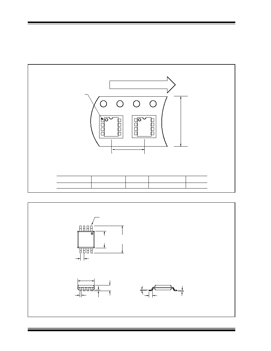
PACKAGING INFORMATION
6.1
Package Marking Information
Package marking data not available at this time.
6.2
Taping Form
6.3
Package Dimensions
Component Taping Orientation for 8-Pin MSOP Devices
Package
Carrier Width (W)
Pitch (P)
Part Per Full Reel
Reel Size
8-Pin MSOP
12 mm
8 mm
2500
13 in
Carrier Tape, Number of Components Per Reel and Reel Size
PIN 1
User Direction of Feed
Standard Reel Component Orientation
for TR Suffix Device
W
P
8-Pin MSOP
.122 (3.10)
.114 (2.90)
.122 (3.10)
.114 (2.90)
.043 (1.10)
MAX.
.006 (0.15)
.002 (0.05)
.016 (0.40)
.010 (0.25)
.197 (5.00)
.189 (4.80)
.008 (0.20)
.005 (0.13)
.028 (0.70)
.016 (0.40)
6
∞ MAX.
.026 (0.65) TYP.
PIN 1
Dimensions: inches (mm)

2002 Microchip Technology Inc.
DS21342B-page9
TC1031
Sales and Support
Data Sheets
Products supported by a preliminary Data Sheet may have an errata sheet describing minor operational differences and recom-
mended workarounds. To determine if an errata sheet exists for a particular device, please contact one of the following:
1.
Your local Microchip sales office
2.
The Microchip Corporate Literature Center U.S. FAX: (480) 792-7277
3.
The Microchip Worldwide Site (www.microchip.com)
Please specify which device, revision of silicon and Data Sheet (include Literature #) you are using.
New Customer Notification System
Register on our web site (www.microchip.com/cn) to receive the most current information on our products.

TC1031
DS21342B-page10
2002 Microchip Technology Inc.
NOTES:

©
2002 Microchip Technology Inc.
DS21342B-page 11
TC1031
Information contained in this publication regarding device
applications and the like is intended through suggestion only
and may be superseded by updates. It is your responsibility to
ensure that your application meets with your specifications.
No representation or warranty is given and no liability is
assumed by Microchip Technology Incorporated with respect
to the accuracy or use of such information, or infringement of
patents or other intellectual property rights arising from such
use or otherwise. Use of Microchip's products as critical com-
ponents in life support systems is not authorized except with
express written approval by Microchip. No licenses are con-
veyed, implicitly or otherwise, under any intellectual property
rights.
Trademarks
The Microchip name and logo, the Microchip logo, FilterLab,
K
EE
L
OQ
, microID,
MPLAB, PIC, PICmicro, PICMASTER,
PICSTART, PRO MATE, SEEVAL and The Embedded Control
Solutions Company are registered trademarks of Microchip Tech-
nology Incorporated in the U.S.A. and other countries.
dsPIC, ECONOMONITOR, FanSense, FlexROM, fuzzyLAB,
In-Circuit Serial Programming, ICSP, ICEPIC, microPort,
Migratable Memory, MPASM, MPLIB, MPLINK, MPSIM,
MXDEV, PICC, PICDEM, PICDEM.net, rfPIC, Select Mode
and Total Endurance are trademarks of Microchip Technology
Incorporated in the U.S.A.
Serialized Quick Turn Programming (SQTP) is a service mark
of Microchip Technology Incorporated in the U.S.A.
All other trademarks mentioned herein are property of their
respective companies.
© 2002, Microchip Technology Incorporated, Printed in the
U.S.A., All Rights Reserved.
Printed on recycled paper.
Microchip received QS-9000 quality system
certification for its worldwide headquarters,
design and wafer fabrication facilities in
Chandler and Tempe, Arizona in July 1999
and Mountain View, California in March 2002.
The Company's quality system processes and
procedures are QS-9000 compliant for its
PICmicro
Æ
8-bit MCUs, K
EE
L
OQ
Æ
code hopping
devices, Serial EEPROMs, microperipherals,
non-volatile memory and analog products. In
addition, Microchip's quality system for the
design and manufacture of development
systems is ISO 9001 certified.

DS21342B-page 12
©
2002 Microchip Technology Inc.
AMERICAS
Corporate Office
2355 West Chandler Blvd.
Chandler, AZ 85224-6199
Tel: 480-792-7200 Fax: 480-792-7277
Technical Support: 480-792-7627
Web Address: http://www.microchip.com
Rocky Mountain
2355 West Chandler Blvd.
Chandler, AZ 85224-6199
Tel: 480-792-7966 Fax: 480-792-7456
Atlanta
500 Sugar Mill Road, Suite 200B
Atlanta, GA 30350
Tel: 770-640-0034 Fax: 770-640-0307
Boston
2 Lan Drive, Suite 120
Westford, MA 01886
Tel: 978-692-3848 Fax: 978-692-3821
Chicago
333 Pierce Road, Suite 180
Itasca, IL 60143
Tel: 630-285-0071 Fax: 630-285-0075
Dallas
4570 Westgrove Drive, Suite 160
Addison, TX 75001
Tel: 972-818-7423 Fax: 972-818-2924
Detroit
Tri-Atria Office Building
32255 Northwestern Highway, Suite 190
Farmington Hills, MI 48334
Tel: 248-538-2250 Fax: 248-538-2260
Kokomo
2767 S. Albright Road
Kokomo, Indiana 46902
Tel: 765-864-8360 Fax: 765-864-8387
Los Angeles
18201 Von Karman, Suite 1090
Irvine, CA 92612
Tel: 949-263-1888 Fax: 949-263-1338
New York
150 Motor Parkway, Suite 202
Hauppauge, NY 11788
Tel: 631-273-5305 Fax: 631-273-5335
San Jose
Microchip Technology Inc.
2107 North First Street, Suite 590
San Jose, CA 95131
Tel: 408-436-7950 Fax: 408-436-7955
Toronto
6285 Northam Drive, Suite 108
Mississauga, Ontario L4V 1X5, Canada
Tel: 905-673-0699 Fax: 905-673-6509
ASIA/PACIFIC
Australia
Microchip Technology Australia Pty Ltd
Suite 22, 41 Rawson Street
Epping 2121, NSW
Australia
Tel: 61-2-9868-6733 Fax: 61-2-9868-6755
China - Beijing
Microchip Technology Consulting (Shanghai)
Co., Ltd., Beijing Liaison Office
Unit 915
Bei Hai Wan Tai Bldg.
No. 6 Chaoyangmen Beidajie
Beijing, 100027, No. China
Tel: 86-10-85282100 Fax: 86-10-85282104
China - Chengdu
Microchip Technology Consulting (Shanghai)
Co., Ltd., Chengdu Liaison Office
Rm. 2401, 24th Floor,
Ming Xing Financial Tower
No. 88 TIDU Street
Chengdu 610016, China
Tel: 86-28-6766200 Fax: 86-28-6766599
China - Fuzhou
Microchip Technology Consulting (Shanghai)
Co., Ltd., Fuzhou Liaison Office
Unit 28F, World Trade Plaza
No. 71 Wusi Road
Fuzhou 350001, China
Tel: 86-591-7503506 Fax: 86-591-7503521
China - Shanghai
Microchip Technology Consulting (Shanghai)
Co., Ltd.
Room 701, Bldg. B
Far East International Plaza
No. 317 Xian Xia Road
Shanghai, 200051
Tel: 86-21-6275-5700 Fax: 86-21-6275-5060
China - Shenzhen
Microchip Technology Consulting (Shanghai)
Co., Ltd., Shenzhen Liaison Office
Rm. 1315, 13/F, Shenzhen Kerry Centre,
Renminnan Lu
Shenzhen 518001, China
Tel: 86-755-2350361 Fax: 86-755-2366086
Hong Kong
Microchip Technology Hongkong Ltd.
Unit 901-6, Tower 2, Metroplaza
223 Hing Fong Road
Kwai Fong, N.T., Hong Kong
Tel: 852-2401-1200 Fax: 852-2401-3431
India
Microchip Technology Inc.
India Liaison Office
Divyasree Chambers
1 Floor, Wing A (A3/A4)
No. 11, O'Shaugnessey Road
Bangalore, 560 025, India
Tel: 91-80-2290061 Fax: 91-80-2290062
Japan
Microchip Technology Japan K.K.
Benex S-1 6F
3-18-20, Shinyokohama
Kohoku-Ku, Yokohama-shi
Kanagawa, 222-0033, Japan
Tel: 81-45-471- 6166 Fax: 81-45-471-6122
Korea
Microchip Technology Korea
168-1, Youngbo Bldg. 3 Floor
Samsung-Dong, Kangnam-Ku
Seoul, Korea 135-882
Tel: 82-2-554-7200 Fax: 82-2-558-5934
Singapore
Microchip Technology Singapore Pte Ltd.
200 Middle Road
#07-02 Prime Centre
Singapore, 188980
Tel: 65-6334-8870 Fax: 65-6334-8850
Taiwan
Microchip Technology Taiwan
11F-3, No. 207
Tung Hua North Road
Taipei, 105, Taiwan
Tel: 886-2-2717-7175 Fax: 886-2-2545-0139
EUROPE
Denmark
Microchip Technology Nordic ApS
Regus Business Centre
Lautrup hoj 1-3
Ballerup DK-2750 Denmark
Tel: 45 4420 9895 Fax: 45 4420 9910
France
Microchip Technology SARL
Parc d'Activite du Moulin de Massy
43 Rue du Saule Trapu
Batiment A - ler Etage
91300 Massy, France
Tel: 33-1-69-53-63-20 Fax: 33-1-69-30-90-79
Germany
Microchip Technology GmbH
Gustav-Heinemann Ring 125
D-81739 Munich, Germany
Tel: 49-89-627-144 0 Fax: 49-89-627-144-44
Italy
Microchip Technology SRL
Centro Direzionale Colleoni
Palazzo Taurus 1 V. Le Colleoni 1
20041 Agrate Brianza
Milan, Italy
Tel: 39-039-65791-1 Fax: 39-039-6899883
United Kingdom
Arizona Microchip Technology Ltd.
505 Eskdale Road
Winnersh Triangle
Wokingham
Berkshire, England RG41 5TU
Tel: 44 118 921 5869 Fax: 44-118 921-5820
03/01/02
*DS21342B*
W
ORLDWIDE
S
ALES
AND
S
ERVICE