
2004 Microchip Technology Inc.
DS21376C-page 1
TC1265
Features
∑ Very Low Dropout Voltage
∑ 800 mA Output Current
∑ High Output Voltage Accuracy
∑ Standard or Custom Output Voltages
∑ Overcurrent and Overtemperature Protection
∑ SHDN Input for Active Power Management
∑ ERROR Output Can Be Used as a Low Battery
Detector (SOIC only)
Applications
∑ Battery-operated Systems
∑ Portable Computers
∑ Medical Instruments
∑ Instrumentation
∑ Cellular/GSM/PHS Phones
∑ Linear Post-Regulators for SMPS
∑ Pagers
Typical Application
Description
The TC1265 is a fixed-output, high-accuracy (typically
±0.5%) CMOS low dropout regulator. Designed
specifically for battery-operated systems, the TC1265's
CMOS construction eliminates wasted ground current,
significantly extending battery life. Total supply current
is typically 80 µA at full load (20 to 60 times lower than
in bipolar regulators).
Key features of the TC1265 include ultra low noise
operation, very low dropout voltage (typically 450 mV
at full load) and fast response to step changes in load.
The TC1265 incorporates both overtemperature and
overcurrent protection. The TC1265 is stable with an
output capacitor of only 1 µF and has a maximum
output current of 800 mA. It is available in 8-Pin SOIC,
5-Pin TO-220 and 5-Pin DDPAK packages.
Package Type
TC1265
V
IN
V
OUT
C
1
1 µF
GND
V
OUT
V
IN
SHDN
SHDN
+
V
IN
GND
V
OU
T
Front View
1 2
3
Tab Is GND
TC1265
1
2
3
4
8
7
6
5
TC1265
NC
SHDN
8-Pin SOIC
GND
NC
BYPASS
V
OUT
V
IN
V
IN
V
OU
T
TC1265
5-Pin TO-220
Tab Is GND
5-Pin DDPAK
1 2 3
GND
SH
D
N
4 5
BY
P
BYP
4
SHDN
5
ERROR
800 mA Fixed-Output CMOS LDO with Shutdown

TC1265
DS21376C-page 2
2004 Microchip Technology Inc.
1.0
ELECTRICAL
CHARACTERISTICS
Absolute Maximum Ratings
Input Voltage .........................................................6.5V
Output Voltage.................. (V
SS
≠ 0.3V) to (V
IN
+ 0.3V)
Power Dissipation................Internally Limited (Note 7)
Maximum Voltage on Any Pin ........V
IN
+0.3V to -0.3V
Operating Temperature Range...... -40∞C < T
J
< 125∞C
Storage Temperature..........................-65∞C to +150∞C
Notice: Stresses above those listed under "Maximum
Ratings" may cause permanent damage to the device. This is
a stress rating only and functional operation of the device at
those or any other conditions above those indicated in the
operation listings of this specification is not implied. Exposure
to maximum rating conditions for extended periods may affect
device reliability.
DC CHARACTERISTICS
Electrical Specifications: Unless otherwise indicated, V
IN
= V
R
+ 1.5V, (Note 1), I
L
= 100 µA, C
L
= 3.3 µF,
SHDN > V
IH
, T
A
= +25∞C. Boldface type specifications apply for junction temperatures of -40∞C to +125∞C.
Parameters
Sym
Min
Typ
Max
Units
Conditions
Input Operating Voltage
V
IN
2.7
--
6.0
V
Note 2
Maximum Output Current
I
OUTMAX
800
--
--
mA
Output Voltage
V
OUT
V
R
≠ 2.5%
V
R
± 0.5% V
R
+ 2.5%
V
V
R
2.5V
V
R
≠ 2%
V
R
± 0.5%
V
R
+ 3%
V
R
= 1.8V
V
OUT
Temperature Coefficient
V
OUT
/
T
--
40
--
ppm/∞C
Note 3
Line Regulation
V
OUT
/
V
IN
--
0.007
0.35
%
(V
R
+ 1V)
V
IN
6V
Load Regulation (Note 4)
V
OUT
/V
OUT
-0.01
0.002
+0.01
%/mA
I
L
= 0.1 mA to I
OUTMAX
Dropout Voltage (Note 5)
V
IN
≠V
OUT
--
20
30
mV
V
R
2.5V, I
L
= 100 µA
--
50
160
I
L
= 100 mA
--
150
480
I
L
= 300 mA
--
260
800
I
L
= 500 mA
--
450
1300
I
L
= 800 mA
--
700
1000
V
R
= 1.8V, I
L
= 500 mA
--
890
1400
I
L
= 800 mA
Supply Current
I
DD
--
80
130
µA
SHDN = V
IH
, I
L
= 0
Shutdown Supply Current
I
SHDN
--
0.05
1
µA
SHDN = 0V
Power Supply Rejection Ratio
PSRR
--
64
--
db
F
1 kHz
Output Short Circuit Current
I
OUTSC
--
1200
1400
mA
V
OUT
= 0V
Thermal Regulation
V
OUT
/
P
D
--
0.04
--
V/W
Note 6
Output Noise
eN
--
260
--
nV/
Hz
I
L
= I
OUTMAX
, F = 10 kH
Z
Note
1: V
R
is the regulator output voltage setting.
2: The minimum V
IN
has to justify the conditions: V
IN
V
R
+ V
DROPOUT
and V
IN
2.7V for I
L
= 0.1 mA to I
OUTMAX
.
3:
4: Regulation is measured at a constant junction temperature using low duty cycle pulse testing. Load regulation is tested
over a load range from 0.1 mA to the maximum specified output current. Changes in output voltage due to heating effects
are covered by the thermal regulation specification.
5: Dropout voltage is defined as the input-to-output differential at which the output voltage drops 2% below its nominal value
measured at a 1.5V differential.
6: Thermal regulation is defined as the change in output voltage at a time T after a change in power dissipation is applied,
excluding load or line regulation effects. Specifications are for a current pulse equal to I
LMAX
at V
IN
= 6V for T = 10 ms.
7: The maximum allowable power dissipation is a function of ambient temperature, the maximum allowable junction temper-
ature and the thermal resistance from junction-to-air (i.e., T
A
, T
J
,
JA
). Exceeding the maximum allowable power dissipa-
tion causes the device to initiate thermal shutdown. Please see Section 5.0 "Thermal Considerations" for more details.
8: Hysteresis voltage is referenced to V
R
.
TCV
OUT
V
OUTMAX
V
OUTMIN
≠
(
)
10
6
≠
V
OUT
T
◊
-------------------------------------------------------------------------
=

2004 Microchip Technology Inc.
DS21376C-page 3
TC1265
SHDN Input
SHDN Input High Threshold
V
IH
45
--
--
%V
IN
SHDN Input Low Threshold
V
IL
--
--
15
%V
IN
ERROR Output (SOIC Only)
Minimum Operating Voltage
V
MIN
1.0
--
--
V
Output Logic Low Voltage
V
OL
--
--
400
mV
1 mA Flows to ERROR
ERROR Threshold Voltage
V
TH
--
0.95 x V
R
--
V
ERROR Positive Hysteresis
V
HYS
--
50
--
mV
Note 8
DC CHARACTERISTICS (CONTINUED)
Electrical Specifications: Unless otherwise indicated, V
IN
= V
R
+ 1.5V, (Note 1), I
L
= 100 µA, C
L
= 3.3 µF,
SHDN > V
IH
, T
A
= +25∞C. Boldface type specifications apply for junction temperatures of -40∞C to +125∞C.
Parameters
Sym
Min
Typ
Max
Units
Conditions
Note
1: V
R
is the regulator output voltage setting.
2: The minimum V
IN
has to justify the conditions: V
IN
V
R
+ V
DROPOUT
and V
IN
2.7V for I
L
= 0.1 mA to I
OUTMAX
.
3:
4: Regulation is measured at a constant junction temperature using low duty cycle pulse testing. Load regulation is tested
over a load range from 0.1 mA to the maximum specified output current. Changes in output voltage due to heating effects
are covered by the thermal regulation specification.
5: Dropout voltage is defined as the input-to-output differential at which the output voltage drops 2% below its nominal value
measured at a 1.5V differential.
6: Thermal regulation is defined as the change in output voltage at a time T after a change in power dissipation is applied,
excluding load or line regulation effects. Specifications are for a current pulse equal to I
LMAX
at V
IN
= 6V for T = 10 ms.
7: The maximum allowable power dissipation is a function of ambient temperature, the maximum allowable junction temper-
ature and the thermal resistance from junction-to-air (i.e., T
A
, T
J
,
JA
). Exceeding the maximum allowable power dissipa-
tion causes the device to initiate thermal shutdown. Please see Section 5.0 "Thermal Considerations" for more details.
8: Hysteresis voltage is referenced to V
R
.
TCV
OUT
V
OUTMAX
V
OUTMIN
≠
(
)
10
6
≠
V
OUT
T
◊
-------------------------------------------------------------------------
=
TEMPERATURE CHARACTERISTICS
Electrical Specifications: Unless otherwise indicated, V
IN
= V
R
+ 1.5V, I
L
= 100 µA, C
L
= 3.3 µF,
SHDN > V
IH
, T
A
= +25∞C.
Parameters
Sym
Min
Typ
Max
Units
Conditions
Temperature Ranges
Specified Temperature Range
T
A
-40
--
+125
∞C
(Note 1)
Operating Temperature Range
T
J
-40
--
+125
∞C
Storage Temperature Range
T
A
-65
--
+150
∞C
Thermal Package Resistances
Thermal Resistance, 5L-DDPAK
JA
--
57
--
∞C/W
Thermal Resistance, 5L-TO-220
JA
--
71
--
∞C/W
Thermal Resistance, 8L-SOIC
JA
--
163
--
∞C/W
Note
1:
Operation in this range must not cause T
J
to exceed Maximum Junction Temperature (+125∞C).

TC1265
DS21376C-page 4
2004 Microchip Technology Inc.
2.0
TYPICAL PERFORMANCE CURVES
FIGURE 2-1:
Line Regulation vs.
Temperature.
FIGURE 2-2:
Output Noise vs. Frequency.
FIGURE 2-3:
Load Regulation vs.
Temperature.
FIGURE 2-4:
I
DD
vs. Temperature.
FIGURE 2-5:
3.0V Dropout Voltage vs.
I
LOAD
.
FIGURE 2-6:
3.0V V
OUT
vs.Temperature.
Note:
The graphs and tables provided following this note are a statistical summary based on a limited number of
samples and are provided for informational purposes only. The performance characteristics listed herein
are not tested or guaranteed. In some graphs or tables, the data presented may be outside the specified
operating range (e.g., outside specified power supply range) and therefore outside the warranted range.
0.020
0.018
0.016
0.012
0.010
0.008
0.006
0.004
0.002
0.000
0.014
TEMPERATURE (
∞
C)
LI
N
E
R
EG
U
L
A
TIO
N
(
%
)
-40
∞
C 0
∞
C
25
∞
C 70
∞
C
85
∞
C 125
∞
C
FREQUENCY (kHz)
NOISE (
µ
V/
Hz)
10.0
1.0
0.01
0.01
1
10
100
1000
0.1
0.0
R
LOAD
= 50
C
OUT
= 1µF
-40∞C
0∞C
25∞C 70∞C
85∞C 125∞C
0.0100
0.0090
0.0080
0.0070
0.0060
0.0050
0.0040
0.0030
0.0020
0.0010
0.0100
TEMPERATURE (∞C)
LOAD REGULATION (%/mA)
1 mA to 800 mA
VOUT
=
3V
TEMPERATURE (∞C)
I DD
(µA)
150
135
120
105
90
75
60
45
30
15
0
-40∞C 0∞C
25∞C 70∞C
85∞C
VOUT = 3V
125∞C
0.600
0.550
0.500
0.450
0.400
0.350
0.300
0.250
0.200
0.150
0.100
0.050
0.000
0 100 200 300 400 500 600 700 800
ILOAD (mA)
DROPOUT VOLTAGE (V)
85∞C
125∞C
-40∞C
0∞C
25∞C
70∞C
3.030
3.020
3.010
3.000
2.990
2.980
2.970
2.960
2.950
2.940
2.930
2.920
TEMPERATURE (∞C)
V
O
U
T
(
V
)
ILOAD = 0.1mA
ILOAD = 300mA
ILOAD = 500mA
ILOAD = 800mA
-40
∞
C 0
∞
C
25
∞
C 70
∞
C
85
∞
C 125
∞
C

2004 Microchip Technology Inc.
DS21376C-page 5
TC1265
2.0
TYPICAL PERFORMANCE CURVES (CONT)
FIGURE 2-1:
I
SHDN
vs. Temperature.
0.090
0.080
0.070
0.060
0.050
0.040
0.030
0.020
0.010
0.000
TEMPERATURE (∞C)
I SHDN (
µ A)
-40∞C
0∞C
25∞C
70∞C
85∞C 125∞C
TC1265
DS21376C-page 6
2004 Microchip Technology Inc.
3.0
PIN DESCRIPTIONS
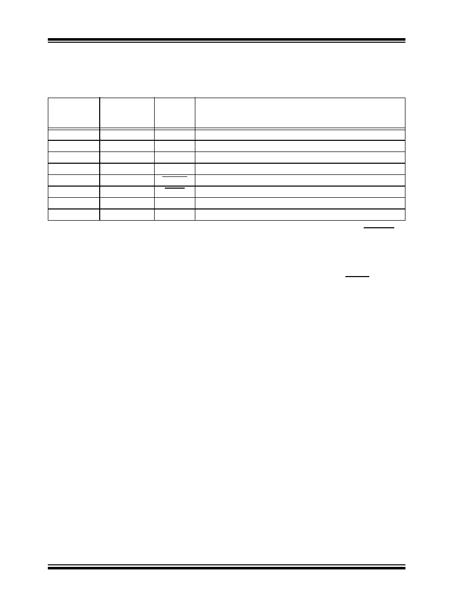
The descriptions of the pins are listed in Table 3-1.
TABLE 3-1:
PIN FUNCTION TABLE
3.1
Regulated Output Voltage (V
OUT
)
Regulated voltage output.
3.2
Ground (GND)
Ground terminal.
3.3
Reference Bypass (BYPASS)
Reference bypass input. Connecting a 470 pF to this
input further reduces output noise.
3.4
Out-of-Regulation Flag (ERROR)
Out-of-regulation flag (open-drain output). This output
goes low when V
OUT
is out-of-tolerance by
approximately -5%.
3.5
Shutdown Control (SHDN)
Shutdown control input. The regulator is fully enabled
when a logic-high is applied to this input. The regulator
enters shutdown when a logic-low is applied to this
input. During shutdown, the output voltage falls to zero
and the supply current is reduced to 0.05 µA (typical).
3.6
Unregulated Supply (V
IN
)
Unregulated supply input.
Pin No.
(8-Pin SOIC)
Pin No.
(5-Pin DDPAK)
(5-Pin TO-220)
Symbol
Description
1
5
V
OUT
Regulated voltage output
2
3
GND
Ground terminal
3
--
NC
No connect
4
1
BYPASS
Reference bypass input
5
--
ERROR
Out-of-Regulation Flag (open drain output)
6
2
SHDN
Shutdown control input
7
--
NC
No connect
8
4
V
IN
Unregulated supply input

2004 Microchip Technology Inc.
DS21376C-page 7
TC1265
4.0
DETAILED DESCRIPTION
The TC1265 is a precision, fixed-output LDO. Unlike
bipolar regulators, the TC1265's supply current does
not increase with load current. In addition, V
OUT
remains stable and within regulation over the entire
0 mA to I
LOADMAX
load current range (an important
consideration in RTC and CMOS RAM battery back-up
applications).
Figure 4-1 shows a typical application circuit.
FIGURE 4-1:
Typical Application Circuit.
4.1
Output Capacitor
A 1 µF (min.) capacitor from V
OUT
to ground is
required. The output capacitor should have an Effective
Series Resistance (ESR) greater than 0.1
and less
than 5
. A 1 µF capacitor should be connected from
V
IN
to GND if there is more than 10 inches of wire
between the regulator and the AC filter capacitor, or if a
battery is used as the power source. Aluminum electro-
lytic or tantalum capacitor types can be used. Since
many aluminum electrolytic capacitors freeze at
approximately -30∞C, solid tantalums are recom-
mended for applications operating below -25∞C. When
operating from sources other than batteries, supply-
noise rejection and transient response can be
improved by increasing the value of the input and
output capacitors, and by employing passive filtering
techniques.
4.2
ERROR Output
ERROR is driven low whenever V
OUT
falls out of
regulation by more than ≠ 5% (typ.). This condition may
be caused by low input voltage, output current limiting,
or thermal limiting. The ERROR threshold is 5% below
rated V
OUT
regardless of the programmed output
voltage value (e.g., ERROR = V
OL
at 4.75V (typ.) for a
5.0V regulator and 2.85V (typ.) for a 3.0V regulator).
ERROR output operation is shown in Figure 4-2.
Note that ERROR is active when V
OUT
is at or below
V
TH
and inactive when V
OUT
is above V
TH
+ V
H
.
As shown in Figure 4-1, ERROR can be used as a
battery low flag or as a processor RESET signal (with
the addition of timing capacitor C
3
). R
1
x C
3
should be
chosen to maintain ERROR below V
IH
of the processor
RESET input for at least 200 ms to allow time for the
system to stabilize. Pull-up resistor R
1
can be tied to
V
OUT
, V
IN
or any other voltage less than (V
IN
+ 0.3V).
FIGURE 4-2:
ERROR Output Operation.
C
1
R
1
1 M
V
+
TC1265
V
IN
Battery
V
OUT
ERROR
SHDN
GND
V
OUT
1 µF
+
+
Shutdown Control
(to CMOS Logic or Tie
to V
IN
, if unused)
C
2
1 µF
+
C
3
Required Only
if ERROR is used as a
Processor RESET Signal
(See Text)
C
3
0.2 µF
+
BATTLOW
or RESET
V
OUT
V
TH
V
IH
Hysteresis (V
H
)
V
OL
ERROR

TC1265
DS21376C-page 8
2004 Microchip Technology Inc.
5.0
THERMAL CONSIDERATIONS
5.1
Thermal Shutdown
Integrated thermal protection circuitry shuts the
regulator off when die temperature exceeds 160∞C.
The regulator remains off until the die temperature
drops to approximately 150∞C.
5.2
Power Dissipation
The amount of power the regulator dissipates is
primarily a function of input voltage, output voltage and
output current. The following equation is used to
calculate worst-case actual power dissipation:
EQUATION 5-1:
The maximum allowable power dissipation
(Equation 5-2) is a function of the maximum ambient
temperature (T
AMAX
), the maximum allowable die
temperature (T
JMAX
) and the thermal resistance from
junction-to-air (
JA
).
EQUATION 5-2:
Table 5-1 and Table 5-2 show various values of
JA
for
the TC1265 package types.
TABLE 5-1:
THERMAL RESISTANCE
GUIDELINES FOR TC1265 IN
8-PIN SOIC PACKAGE
TABLE 5-2:
THERMAL RESISTANCE
GUIDELINES FOR TC1265 IN
5-PIN DDPAK/TO-220
PACKAGE
Equation 5-1 can be used in conjunction with
Equation 5-2 to ensure regulator thermal operation is
within limits. For example:
Find:
1.
Actual power dissipation
2.
Maximum allowable dissipation
Actual power dissipation:
Maximum allowable power dissipation:
In this example, the TC1265 dissipates a maximum of
260 mW, below the allowable limit of 500 mW. In a
similar manner, Equation 5-1 and Equation 5-2 can be
used to calculate maximum current and/or input
voltage limits. For example, the maximum allowable
V
IN
is found by substituting the maximum allowable
power dissipation of 500 mW into Equation 5-1, from
which V
INMAX
= 4.6V.
Copper
Area
(Topside)*
Copper
Area
(Backside)
Board
Area
Thermal
Resistance
(
JA
)
2500 sq mm
2500 sq mm
2500 sq mm
60∞C/W
1000 sq mm
2500 sq mm
2500 sq mm
60∞C/W
225 sq mm
2500 sq mm
2500 sq mm
68∞C/W
100 sq mm
2500 sq mm
2500 sq mm
74∞C/W
* Pin 2 is ground. Device is mounted on the top-side.
Where:
V
INMAX
V
OUTMIN
I
LOADMAX
P
D
= Worst-case actual power dissipation
= Minimum regulator output voltage
= Maximum output (load) current
= Maximum voltage on V
IN
P
D
V
IN MAX
V
OUTMIN
≠
(
)
I
LOA DMAX
=
Where:
V
INMAX
V
OUTMIN
I
LOADMAX
P
D
= Worst-case actual power dissipation
= Minimum regulator output voltage
= Maximum output (load) current
= Maximum voltage on V
IN
P
DMAX
T
JMAX
T
AMAX
≠
JA
---------------------------------------
=
Copper
Area
(Topside)*
Copper
Area
(Backside)
Board
Area
Thermal
Resistance
(
JA
)
2500 sq mm
2500 sq mm 2500 sq mm
25∞C/W
1000 sq mm
2500 sq mm 2500 sq mm
27∞C/W
125 sq mm
2500 sq mm 2500 sq mm
35∞C/W
* Tab of device attached to top-side copper
Given:
V
INMAX
= 3.3V ± 10%
V
OUTMIN
= 2.7V ± 0.5%
I
LOADMAX
= 275 mA
T
JMAX
= 125∞C
T
AMAX
= 95∞C
JA
= 60∞C/W (SOIC)
P
D
V
INMAX
V
OUTMIN
≠
(
)
I
LOADMAX
P
D
3.3
1.1
◊
(
)
2.7
.995
◊
(
)
≠
275
10
3
≠
◊
=
P
D
260 mW
=
P
DMAX
T
JMAX
T
AMAX
≠
JA
---------------------------------------
=
P
DMAX
125
95
≠
(
)
60
-------------------------
=
P
DMAX
500 mW
=

2004 Microchip Technology Inc.
DS21376C-page 9
TC1265
6.0
PACKAGING INFORMATION
6.1
Package Marking Information
Legend: XX...X
Customer specific information*
YY
Year code (last 2 digits of calendar year)
WW
Week code (week of January 1 is week `01')
NNN
Alphanumeric traceability code
Note:
In the event the full Microchip part number cannot be marked on one line, it will
be carried over to the next line thus limiting the number of available characters
for customer specific information.
*
Standard OTP marking consists of Microchip part number, year code, week code, and traceability code.
XXXXXXXXX
XXXXXXXXX
YYWWNNN
5-Lead DDPAK
TC1265
3.3VET
Example
5-Lead TO-220
XXXXXXXXX
XXXXXXXXX
YYWWNNN
Example:
TC1265-
3.3VAT
X
0430256
8-Lead SOIC (150 mil)
Example:
XXXXXXXX
XXXXYYWW
NNN
1265-3.3
VOA0430
256
0430256

TC1265
DS21376C-page 10
2004 Microchip Technology Inc.
5-Lead Plastic (ET) (DDPAK)
BOTTOM VIEW
TOP VIEW
E
D
b
E1
D2
A
A1
c2
c
L
D1
e
1
(5X)
L3
1
ß Significant Characteristic
Drawing No. C04-012
Notes:
Mold Draft Angle
Dimensions D and E do not include mold flash or protrusions. Mold flash or protrusions shall not
exceed .010" (0.254mm) per side.
1
7∞
Pitch
Number of Pins
Overall Width
Standoff ß
Molded Package Length
Exposed Pad Width
Overall Height
MAX
Units
Dimension Limits
A1
E1
D
E
e
A
.398
.000
.256 REF
INCHES*
.067 BSC
MIN
5
NOM
MAX
.010
0.00
10.11
6.50 REF
MILLIMETERS
.183
MIN
5
1.70 BSC
NOM
0.25
4.65
JEDEC equivalent: TO-252
4.50
.170
.005
0.13
Foot Length
L
.068
.089
.110
1.73
2.26
2.79
Foot Angle
--
--
8∞
.177
*Controlling Parameter
4.32
.385
.410
9.78
10.41
.330
.350
.370
8.38
8.89
9.40
Overall Length
D1
.549
.577
.605
13.94
14.66
15.37
Lead Thickness
c
.014
.020
.026
0.36
0.51
0.66
Pad Thickness
c2
.045
--
.055
1.14
--
1.40
Lead Width
.037
b
.026
.032
0.66
0.81
0.94
3∞
--
8∞
7∞
3∞
--
--
--
Exposed Pad Length
D2
.303 REF
7.75 REF
Pad Length
L3
.045
--
.067
1.14
--
1.70

2004 Microchip Technology Inc.
DS21376C-page 11
TC1265
5-Lead Plastic Transistor Outline (AT) (TO-220)
L
H1
Q
E
b
e1
e
C1
J1
F
A
D
a
(5X)
ÿP
EJECTOR PIN
e3
Drawing No. C04-036
Notes:
Dimensions D and E1 do not include mold flash or protrusions. Mold flash or
protrusions shall not exceed .010" (0.254mm) per side.
JEDEC equivalent: TO-220
*Controlling Parameter
Mold Draft Angle
Lead Width
Lead Thickness
a
C1
b
.014
Dimension Limits
Overall Height
Lead Length
Overall Width
Lead Pitch
A
L
E
.540
MIN
e
Units
.060
INCHES*
.022
0.36
0.56
MILLIMETERS
.190
.560
13.72
MIN
MAX
4.83
14.22
MAX
.160
4.06
3∞
7∞
3∞
7∞
Overall Length
D
1.02
0.64
.040
.025
Overall Lead Centers
e1
.263
.385
.560
.273
6.68
6.93
.072
1.52
1.83
.415
9.78
10.54
.590
14.22
14.99
Through Hole Diameter
P
.146
.156
3.71
3.96
J1
Base to Bottom of Lead
.090
2.29
.115
2.92
Through Hole Center
Q
.103
2.87
.113
2.62
Flag Thickness
F
.045
1.40
.055
1.14
Flag Length
H1
.234
6.55
.258
5.94
Space Between Leads
e3
.030
1.02
.040
0.76
TC1265
DS21376C-page 12
2004 Microchip Technology Inc.
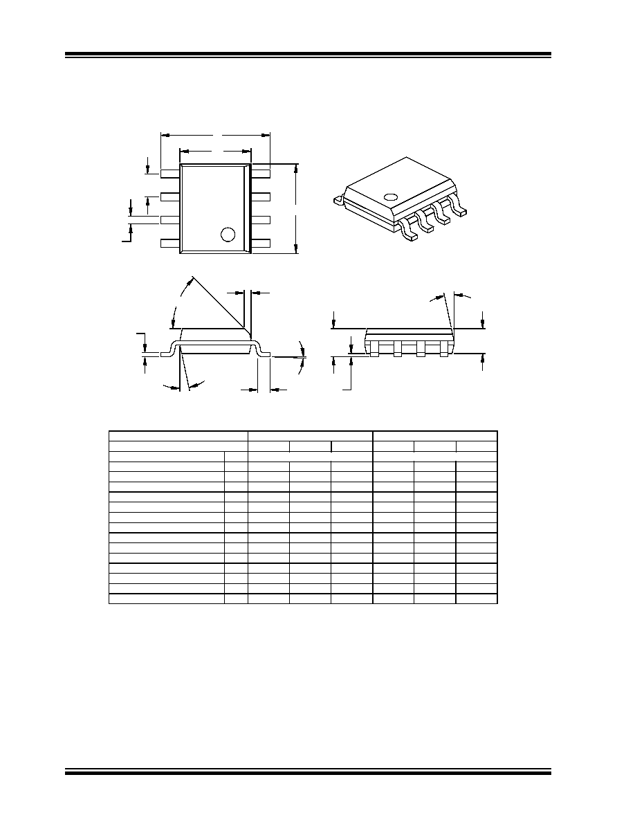
8-Lead Plastic Small Outline (SN) ≠ Narrow, 150 mil Body (SOIC)
Foot Angle
0
4
8
0
4
8
15
12
0
15
12
0
Mold Draft Angle Bottom
15
12
0
15
12
0
Mold Draft Angle Top
0.51
0.42
0.33
.020
.017
.013
B
Lead Width
0.25
0.23
0.20
.010
.009
.008
c
Lead Thickness
0.76
0.62
0.48
.030
.025
.019
L
Foot Length
0.51
0.38
0.25
.020
.015
.010
h
Chamfer Distance
5.00
4.90
4.80
.197
.193
.189
D
Overall Length
3.99
3.91
3.71
.157
.154
.146
E1
Molded Package Width
6.20
6.02
5.79
.244
.237
.228
E
Overall Width
0.25
0.18
0.10
.010
.007
.004
A1
Standoff
ß
1.55
1.42
1.32
.061
.056
.052
A2
Molded Package Thickness
1.75
1.55
1.35
.069
.061
.053
A
Overall Height
1.27
.050
p
Pitch
8
8
n
Number of Pins
MAX
NOM
MIN
MAX
NOM
MIN
Dimension Limits
MILLIMETERS
INCHES*
Units
2
1
D
n
p
B
E
E1
h
L
c
45
∞
A2
A
A1
* Controlling Parameter
Notes:
Dimensions D and E1 do not include mold flash or protrusions. Mold flash or protrusions shall not exceed
.010" (0.254mm) per side.
JEDEC Equivalent: MS-012
Drawing No. C04-057
ß Significant Characteristic

2004 Microchip Technology Inc.
DS21376C-page 13
TC1265
PRODUCT IDENTIFICATION SYSTEM
To order or obtain information, e.g., on pricing or delivery, refer to the factory or the listed sales office
.
Sales and Support
PART NO.
X.XX
XX
Package
Voltage
Option
Device
Device
TC1265 Fixed Output CMOS LDO with Shutdown
Voltage Option:*
1.8V
=
1.8V
2.5V
=
2.5V
3.0V
=
3.0V
3.3V
=
3.3V
* Other output voltages are available. Please contact your
local Microchip sales office for details.
Package
AT
=
Plastic (TO-220), 5-Lead
ET
=
Plastic Transistor Outline (DDPAK), 5-Lead
ETTR
=
Plastic Transistor Outline (DDPAK), 5-Lead,
Tape and Reel
OA
=
Plastic SOIC, (150 mil Body), 8-lead
OATR =
Plastic SOIC, (150 mil Body), 8-lead,
Tape and Reel
Examples:
a)
TC1265-1.8VAT
1.8V LDO, TO-220-5 pkg.
b)
TC1265-2.5VAT
2.5V LDO, TO-220-5 pkg.
c)
TC1265-3.0VAT
3.0V LDO, TO-220-5 pkg.
d)
TC1265-3.3VAT
3.3V LDO, TO-220-5 pkg.
a)
TC1265-1.8VETTR 1.8V LDO, DDPAK-5 pkg.,
Tape and Reel
b)
TC1265-2.5VETTR 2.5V LDO, DDPAK-5 pkg.,
Tape and Reel
c)
TC1265-3.0VETTR 3.0V LDO, DDPAK-5 pkg.,
Tape and Reel
d)
TC1265-3.3VETTR 3.3V LDO, DDPAK-5 pkg.,
Tape and Reel
a)
TC1265-1.8VOA
1.8V LDO, SOIC-8 pkg.
b)
TC1265-1.8VOATR 1.8V LDO, SOIC-8 pkg.,
Tape and Reel
c)
TC1265-2.5VOA
2.5V LDO, SOIC-8 pkg.
d)
TC1265-2.5VOATR 2.5V LDO, SOIC-8 pkg.,
Tape and Reel
e)
TC1265-3.0VOA
3.0V LDO, SOIC-8 pkg.
f)
TC1265-3.0VOATR 3.0V LDO, SOIC-8 pkg.,
Tape and Reel
g)
TC1265-3.3VOA
3.3V LDO, SOIC-8 pkg.
h)
TC1265-3.3VOATR 3.3V LDO, SOIC-8 pkg.,
Tape and Reel
XX
Tape and
Reel
Data Sheets
Products supported by a preliminary Data Sheet may have an errata sheet describing minor operational differences and
recommended workarounds. To determine if an errata sheet exists for a particular device, please contact one of the following:
1.
Your local Microchip sales office
2.
The Microchip Worldwide Site (www.microchip.com)
Please specify which device, revision of silicon and Data Sheet (include Literature #) you are using.
Customer Notification System
Register on our web site (www.microchip.com) to receive the most current information on our products.

TC1265
DS21376C-page 14
2004 Microchip Technology Inc.
NOTES:

2004 Microchip Technology Inc.
DS21376C-page 15
Information contained in this publication regarding device
applications and the like is provided only for your convenience
and may be superseded by updates. It is your responsibility to
ensure that your application meets with your specifications.
MICROCHIP MAKES NO REPRESENTATIONS OR WAR-
RANTIES OF ANY KIND WHETHER EXPRESS OR IMPLIED,
WRITTEN OR ORAL, STATUTORY OR OTHERWISE,
RELATED TO THE INFORMATION, INCLUDING BUT NOT
LIMITED TO ITS CONDITION, QUALITY, PERFORMANCE,
MERCHANTABILITY OR FITNESS FOR PURPOSE.
Microchip disclaims all liability arising from this information and
its use. Use of Microchip's products as critical components in
life support systems is not authorized except with express
written approval by Microchip. No licenses are conveyed,
implicitly or otherwise, under any Microchip intellectual property
rights.
Trademarks
The Microchip name and logo, the Microchip logo, Accuron,
dsPIC, K
EE
L
OQ
, micro
ID
, MPLAB, PIC, PICmicro,
PICSTART, PRO MATE, PowerSmart, rfPIC, and
SmartShunt are registered trademarks of Microchip
Technology Incorporated in the U.S.A. and other countries.
AmpLab, FilterLab, MXDEV, MXLAB, PICMASTER, SEEVAL,
SmartSensor and The Embedded Control Solutions Company
are registered trademarks of Microchip Technology
Incorporated in the U.S.A.
Analog-for-the-Digital Age, Application Maestro, dsPICDEM,
dsPICDEM.net, dsPICworks, ECAN, ECONOMONITOR,
FanSense, FlexROM, fuzzyLAB, In-Circuit Serial
Programming, ICSP, ICEPIC, Migratable Memory, MPASM,
MPLIB, MPLINK, MPSIM, PICkit, PICDEM, PICDEM.net,
PICLAB, PICtail, PowerCal, PowerInfo, PowerMate,
PowerTool, rfLAB, rfPICDEM, Select Mode, Smart Serial,
SmartTel and Total Endurance are trademarks of Microchip
Technology Incorporated in the U.S.A. and other countries.
SQTP is a service mark of Microchip Technology Incorporated
in the U.S.A.
All other trademarks mentioned herein are property of their
respective companies.
© 2004, Microchip Technology Incorporated, Printed in the
U.S.A., All Rights Reserved.
Printed on recycled paper.
Note the following details of the code protection feature on Microchip devices:
∑
Microchip products meet the specification contained in their particular Microchip Data Sheet.
∑
Microchip believes that its family of products is one of the most secure families of its kind on the market today, when used in the
intended manner and under normal conditions.
∑
There are dishonest and possibly illegal methods used to breach the code protection feature. All of these methods, to our
knowledge, require using the Microchip products in a manner outside the operating specifications contained in Microchip's Data
Sheets. Most likely, the person doing so is engaged in theft of intellectual property.
∑
Microchip is willing to work with the customer who is concerned about the integrity of their code.
∑
Neither Microchip nor any other semiconductor manufacturer can guarantee the security of their code. Code protection does not
mean that we are guaranteeing the product as "unbreakable."
Code protection is constantly evolving. We at Microchip are committed to continuously improving the code protection features of our
products. Attempts to break Microchip's code protection feature may be a violation of the Digital Millennium Copyright Act. If such acts
allow unauthorized access to your software or other copyrighted work, you may have a right to sue for relief under that Act.
Microchip received ISO/TS-16949:2002 quality system certification for
its worldwide headquarters, design and wafer fabrication facilities in
Chandler and Tempe, Arizona and Mountain View, California in
October 2003. The Company's quality system processes and
procedures are for its PICmicro
Æ
8-bit MCUs, K
EE
L
OQ
Æ
code hopping
devices, Serial EEPROMs, microperipherals, nonvolatile memory and
analog products. In addition, Microchip's quality system for the design
and manufacture of development systems is ISO 9001:2000 certified.

DS21376C-page 16
2004 Microchip Technology Inc.
AMERICAS
Corporate Office
2355 West Chandler Blvd.
Chandler, AZ 85224-6199
Tel: 480-792-7200
Fax: 480-792-7277
Technical Support:
http://support.microchip.com
Web Address:
www.microchip.com
Atlanta
Alpharetta, GA
Tel: 770-640-0034
Fax: 770-640-0307
Boston
Westford, MA
Tel: 978-692-3848
Fax: 978-692-3821
Chicago
Itasca, IL
Tel: 630-285-0071
Fax: 630-285-0075
Dallas
Addison, TX
Tel: 972-818-7423
Fax: 972-818-2924
Detroit
Farmington Hills, MI
Tel: 248-538-2250
Fax: 248-538-2260
Kokomo
Kokomo, IN
Tel: 765-864-8360
Fax: 765-864-8387
Los Angeles
Mission Viejo, CA
Tel: 949-462-9523
Fax: 949-462-9608
San Jose
Mountain View, CA
Tel: 650-215-1444
Fax: 650-961-0286
Toronto
Mississauga, Ontario,
Canada
Tel: 905-673-0699
Fax: 905-673-6509
ASIA/PACIFIC
Australia - Sydney
Tel: 61-2-9868-6733
Fax: 61-2-9868-6755
China - Beijing
Tel: 86-10-8528-2100
Fax: 86-10-8528-2104
China - Chengdu
Tel: 86-28-8676-6200
Fax: 86-28-8676-6599
China - Fuzhou
Tel: 86-591-8750-3506
Fax: 86-591-8750-3521
China - Hong Kong SAR
Tel: 852-2401-1200
Fax: 852-2401-3431
China - Shanghai
Tel: 86-21-5407-5533
Fax: 86-21-5407-5066
China - Shenyang
Tel: 86-24-2334-2829
Fax: 86-24-2334-2393
China - Shenzhen
Tel: 86-755-8203-2660
Fax: 86-755-8203-1760
China - Shunde
Tel: 86-757-2839-5507
Fax: 86-757-2839-5571
China - Qingdao
Tel: 86-532-502-7355
Fax: 86-532-502-7205
ASIA/PACIFIC
India - Bangalore
Tel: 91-80-2229-0061
Fax: 91-80-2229-0062
India - New Delhi
Tel: 91-11-5160-8631
Fax: 91-11-5160-8632
Japan - Kanagawa
Tel: 81-45-471- 6166
Fax: 81-45-471-6122
Korea - Seoul
Tel: 82-2-554-7200
Fax: 82-2-558-5932 or
82-2-558-5934
Singapore
Tel: 65-6334-8870
Fax: 65-6334-8850
Taiwan - Kaohsiung
Tel: 886-7-536-4818
Fax: 886-7-536-4803
Taiwan - Taipei
Tel: 886-2-2500-6610
Fax: 886-2-2508-0102
Taiwan - Hsinchu
Tel: 886-3-572-9526
Fax: 886-3-572-6459
EUROPE
Austria - Weis
Tel: 43-7242-2244-399
Fax: 43-7242-2244-393
Denmark - Ballerup
Tel: 45-4450-2828
Fax: 45-4485-2829
France - Massy
Tel: 33-1-69-53-63-20
Fax: 33-1-69-30-90-79
Germany - Ismaning
Tel: 49-89-627-144-0
Fax: 49-89-627-144-44
Italy - Milan
Tel: 39-0331-742611
Fax: 39-0331-466781
Netherlands - Drunen
Tel: 31-416-690399
Fax: 31-416-690340
England - Berkshire
Tel: 44-118-921-5869
Fax: 44-118-921-5820
W
ORLDWIDE
S
ALES
AND
S
ERVICE
10/20/04