
2002 Microchip Technology Inc.
DS21391B-page 1
M
TC1412/TC1412N
Features
∑ Latch-Up Protected: Will Withstand 500mA
Reverse Current
∑ Input Will Withstand Negative Inputs Up to 5V
∑ ESD Protected: 4kV
∑ High Peak Output Current: 2A
∑ Wide Operating Range
- 4.5V to 16V
∑ High Capacitive Load Drive Capability: 1000pF in
18nsec
∑ Short Delay Time: 35nsec Typ
∑ Consistent Delay Times With Changes in Supply
Voltage
∑ Matched Delay Times
∑ Low Supply Current
- With Logic "1" Input: 500
µ
A
- With Logic "0" Input: 100
µ
A
∑ Low Output Impedance: 4
∑ Pinout Same as TC1410/TC1411/TC1413
Applications
∑ Switch Mode Power Supplies
∑ Pulse Transformer Drive
∑ Line Drivers
∑ Relay Driver
Device Selection Table
Package Type
General Description
The TC1412/TC1412N are 2A CMOS buffer/drivers.
They will not latch up under any conditions within their
power and voltage ratings. They are not subject to
damage when up to 5V of noise spiking of either
polarity occurs on the ground pin. They can accept,
without damage or logic upset, up to 500mA of current
of either polarity being forced back into their output. All
terminals are fully protected against up to 4kV of
electrostatic discharge.
As MOSFET drivers, the TC1412/TC1412N can easily
charge a 1000pF gate capacitance in 18nsec with
matched rise and fall times, and provide low enough
impedance in both the ON and the OFF states to
ensure the MOSFET's intended state will not be
affected, even by large transients. The rise and fall time
edges are matched to allow driving short-duration
inputs with greater accuracy.
Part Number
Package
Temp. Range
TC1412COA
8-Pin SOIC
0∞C to +70∞C
TC1412CPA
8-Pin PDIP
0∞C to +70∞C
TC1412EOA
8-Pin SOIC
-40∞C to +85∞C
TC1412EPA
8-Pin PDIP
-40∞C to +85∞C
TC1412NCOA
8-Pin SOIC
0∞C to +70∞C
TC1412NCPA
8-Pin PDIP
0∞C to +70∞C
TC1412NEOA
8-Pin SOIC
-40∞C to +85∞C
TC1412NEPA
8-Pin PDIP
-40∞C to +85∞C
TC1412
1
2
3
4
V
DD
5
6
7
8
OUT
GND
V
DD
IN
NC
GND
NC = No internal connection
2
6, 7
Inverting
OUT
TC1412N
1
2
3
4
V
DD
5
6
7
8
OUT
GND
V
DD
IN
NC
GND
2
6, 7
Noninverting
OUT
8-Pin PDIP/SOIC
2A High-Speed MOSFET Drivers
TC1412/TC1412N
DS21391B-page 2
2002 Microchip Technology Inc.
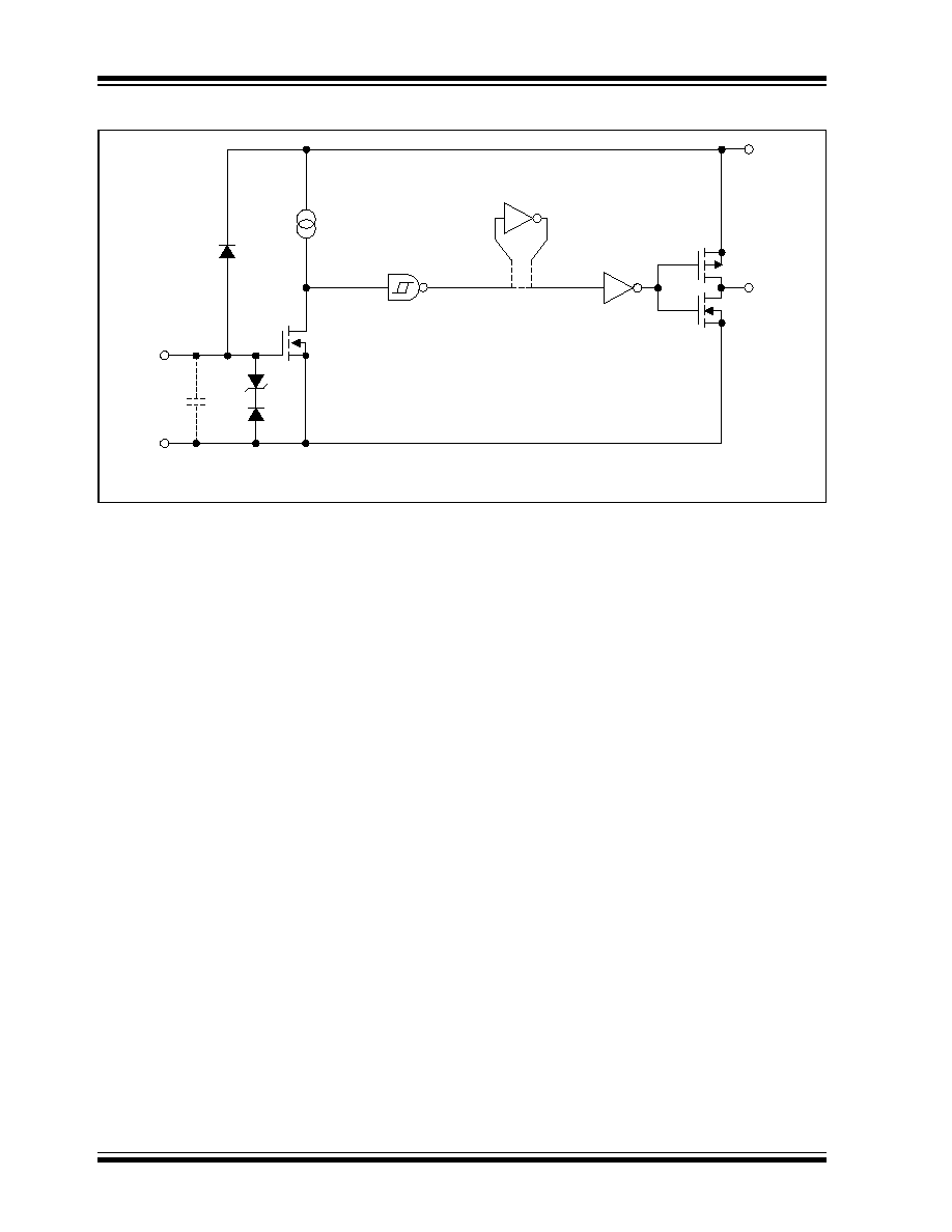
Functional Block Diagram
Output
Input
GND
Effective
Input
C = 10pF
300mV
Inverting
Outputs
Noninverting
Outputs
V
DD
TC1412N
4.7V
TC1412
2002 Microchip Technology Inc.
DS21391B-page 3
TC1412/TC1412N
1.0
ELECTRICAL
CHARACTERISTICS
Absolute Maximum Ratings*
Supply Voltage..................................................... +20V
Input Voltage...................... V
DD
+ 0.3V to GND ≠ 5.0V
Power Dissipation (T
A
70∞C)
PDIP ........................................................ 730mW
SOIC........................................................ 470mW
Package Thermal Resistance
PDIP R
J-A
..............................................125
∞
C/W
PDIP R
J-C
............................................... 42∞C/W
SOIC R
J-A
............................................ 155∞C/W
SOIC R
J-C
.............................................. 45∞C/W
Operating Temperature Range
C Version .........................................0∞C to +70∞C
E Version ..................................... -40∞C to +85∞C
Storage Temperature Range ............. -65∞C to +150∞C
*Stresses above those listed under "Absolute Maximum
Ratings" may cause permanent damage to the device. These
are stress ratings only and functional operation of the device
at these or any other conditions above those indicated in the
operation sections of the specifications is not implied.
Exposure to Absolute Maximum Rating conditions for
extended periods may affect device reliability.
TC1412/TC1412N ELECTRICAL SPECIFICATIONS
Electrical Characteristics: Over operating temperature range with 4.5V
V
DD
16V, unless otherwise noted. Typical values are
measured at T
A
= +25∞C, V
DD
= 16V.
Symbol
Parameter
Min
Typ
Max
Units
Test Conditions
Input
V
IH
Logic 1, High Input Voltage
2.0
--
--
V
V
IL
Logic 0, Low Input Voltage
--
--
0.8
V
I
IN
Input Current
-1
-10
--
--
1
10
µ
A
0V
V
IN
V
DD,
T
A
= +25∞C
-40∞C
T
A
+85∞C
Output
V
OH
High Output Voltage
V
DD
≠ 0.025
--
--
V
DC Test
V
OL
Low Output Voltage
--
--
0.025
V
DC Test
R
O
Output Resistance
--
4
5
5
6
7
7
V
DD
= 16V, I
O
= 10mA, T
A
= +25∞C,
0∞C
T
A
+70∞C
-40∞C
T
A
+85∞C
I
PK
Peak Output Current
--
2.0
--
A
V
DD
= 16V
I
REV
Latch-Up Protection
Withstand Reverse Current
--
0.5
--
A
Duty cycle
2%, t
300
µ
sec,
V
DD
= 16V

TC1412/TC1412N
DS21391B-page 4
2002 Microchip Technology Inc.
TC1412/TC1412N ELECTRICAL SPECIFICATIONS (CONTINUED)
Electrical Characteristics: Over operating temperature range with 4.5V
V
DD
16V, unless otherwise noted. Typical values are
measured at T
A
= +25∞C, V
DD
= 16V.
Symbol
Parameter
Min
Typ
Max
Units
Test Conditions
Switching Time (Note 1)
t
R
Rise Time
--
18
20
22
26
31
31
nsec
T
A
= +25∞C,
0∞C
T
A
+70∞C
-40∞C
T
A
+85∞C, Figure 3-2
t
F
Fall Time
--
18
20
22
26
31
31
nsec
T
A
= +25∞C,
0∞C
T
A
+70∞C
-40∞C
T
A
+85∞C, Figure 3-2
t
D1
Delay Time
--
35
40
40
45
50
50
nsec
T
A
= +25∞C,
0∞C
T
A
+70∞C
-40∞C
T
A
+85∞C, Figure 3-2
t
D2
Delay Time
--
35
40
40
45
50
50
nsec
T
A
= +25∞C,
0∞C
T
A
+70∞C
-40∞C
T
A
+85∞C, Figure 3-2
Power Supply
I
S
Power Supply Current
--
--
0.5
0.1
1.0
0.15
mA
V
IN
= 3V, V
DD
= 16V
V
IN
= 0V
Note
1:
Switching times ensured by design.

2002 Microchip Technology Inc.
DS21391B-page 5
TC1412/TC1412N
2.0
PIN DESCRIPTIONS
The descriptions of the pins are listed in Table 2-1.
TABLE 2-1:
PIN FUNCTION TABLE
Pin No.
(8-Pin PDIP,
SOIC)
Symbol
Description
1
V
DD
Supply input, 4.5V to 16V.
2
INPUT
Control input.
3
NC
No connection.
4
GND
Ground.
5
GND
Ground.
6
OUTPUT
CMOS totem-pole output, common to pin 7.
7
OUTPUT
CMOS totem-pole output, common to pin 6.
8
V
DD
Supply Input, 4.5V to 16V.