 | –≠–ª–µ–∫—Ç—Ä–æ–Ω–Ω—ã–π –∫–æ–º–ø–æ–Ω–µ–Ω—Ç: TC2117 | –°–∫–∞—á–∞—Ç—å:  PDF PDF  ZIP ZIP |
©
2002 Microchip Technology Inc.
DS21665B-page 1
TC2117
Features
∑ Fixed Output Voltages: 1.8V, 2.5V, 3.0V, 3.3V
∑ Very Low Dropout Voltage
∑ Rated 800mA Output Current
∑ High Output Voltage Accuracy
∑ Standard or Custom Output Voltages
∑ Over-Current and Over-Temperature Protection
∑ Space Saving SOT-223 Package
Applications
∑ 5V to 3.3V Linear Regulator
∑ Portable Computers
∑ Instrumentation
∑ Battery Operated Systems
∑ Linear Post-Regulator for SMPS
∑ Core Voltage Supply for FPGAs, PLDs, CPUs,
DSPs
Device Selection Table
Note: xx indicates output voltages.
Available Output Voltages: 1.8, 2.5, 3.0, 3.3.
Other output voltages are available. Please contact Microchip
Technology Inc. for details.
Package Type
General Description
The TC2117 is a fixed, high accuracy (typically ±0.5%)
CMOS low dropout regulator. Designed specifically for
battery operated systems, the TC2117's CMOS con-
struction eliminates wasted ground current, signifi-
cantly extending battery life. Total supply current is
typically 80
µ
A at full load (20 to 60 times lower than in
bipolar regulators).
TC2117 key features include ultra low noise, very low
dropout voltage (typically 450mV at full load), and fast
response to step changes in load. The TC2117 incor-
porates both over-temperature and over-current pro-
tection. The TC2117 is stable with an output capacitor
of only 1
µ
F and has a maximum output current of
800mA. This device is available in 3-Pin SOT-223, and
3-Pin DDPAK packages.
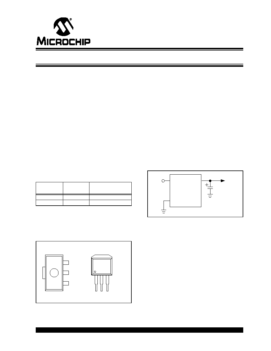
Typical Application
Part Number
Package
Junction
Temperature Range
TC2117-xxVDB 3-Pin SOT-223
-40∞C to +125∞C
TC2117-xxVEB
3-Pin DDPAK
-40∞C to +125∞C
V
IN
V
IN
V
OUT
GND
GND
V
OUT
Tab is V
OUT
Front View
Front View
1
1
2
3
3
2
Tab is V
OUT
TC2117
TC2117
3-Pin SOT-223
3-Pin DDPAK
TC2117
V
IN
V
OUT
C1
1
µF
GND
V
OUT
V
IN
800mA Fixed Low Dropout Positive Regulator
TC2117
DS21665B-page 2
©
2002 Microchip Technology Inc.
1.0
ELECTRICAL
CHARACTERISTICS
Absolute Maximum Ratings*
Input Voltage .........................................................6.5V
Output Voltage.................... (V
SS
≠ 0.3) to (V
IN
+ 0.3V)
Power Dissipation................Internally Limited (Note 7)
Maximum Voltage on Any Pin ......... V
IN
+0.3V to -0.3V
Operating Temperature ............... -40∞C < T
J
< +125∞C
Storage temperature .......................... -65∞C to +150∞C
*Stresses above those listed under "Absolute Maximum
Ratings" may cause permanent damage to the device. These
are stress ratings only and functional operation of the device
at these or any other conditions above those indicated in the
operation sections of the specifications is not implied.
Exposure to Absolute Maximum Rating conditions for
extended periods may affect device reliability.
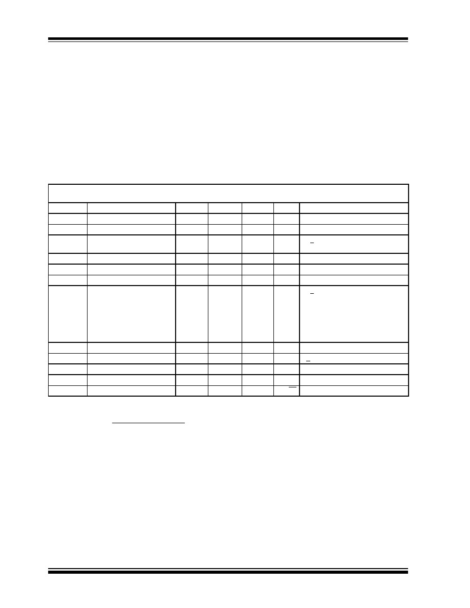
TC2117 ELECTRICAL SPECIFICATIONS
Electrical Characteristics: V
IN
= V
R
+ 1.5V (Note 1), I
L
= 100
µ
A, C
L
= 3.3
µ
F, T
A
= 25∞C, unless otherwise specified. Boldface type
specifications apply for junction temperatures of -40∞C to +125∞C.
Symbol
Parameter
Min
Typ
Max
Units
Test Conditions
V
IN
Input Operating Voltage
2.7
--
6.0
V
(Note 2)
I
OUT
MAX
Maximum Output Current
800
--
--
mA
V
OUT
Output Voltage
V
R
≠ 2.5%
V
R
≠ 2%
V
R
≠ 0.5%
V
R
≠ 0.5%
V
R
+ 2.5%
V
R
+ 3%
V
V
R
> 2.5V
V
R
= 1.8V
V
OUT
/
T
V
OUT
Temperature Coefficient
--
40
--
ppm/∞C (Note 3)
V
OUT
/
V
IN
Line Regulation
--
0.007
0.35
%
(V
R
+ 1V) V
IN
6V
V
OUT
/V
OUT
Load Regulation
-0.01
0.002
0
%/mA
I
L
= 0.1mA to I
OUT
MAX
(Note 4)
V
IN
- V
OUT
Dropout Voltage
--
--
--
--
--
--
--
20
60
190
340
600
700
890
30
160
480
800
1300
1000
1400
mV
V
R
> 2.5V,
I
L
= 100
µ
A
I
L
= 100
µ
A
I
L
= 300
µ
A
I
L
= 500
µ
A
I
L
= 800
µ
A
V
R
= 1.8V,
I
L
= 500
µ
A
I
L
= 800
µ
A (Note 5)
I
DD
Supply Current
--
80
130
µ
A
I
L
= 0
PSRR
Power Supply Rejection Ratio
--
55
--
dB
F < 120Hz
I
OUT
SC
Output Short Circuit Current
--
1200
--
mA
V
OUT
= 0V
V
OUT
/
P
D
Thermal Regulation
--
0.04
--
V/W
(Note 6)
eN
Output Noise
--
300
--
nV/
Hz I
L
= 100mA, F = 10kHz
Note
1:
V
R
is the regulator output voltage setting.
2:
The minimum V
IN
has to justify the conditions: V
IN
V
R
+ V
DROPOUT
and V
IN
2.7V for I
L
= 0.1mA to I
OUT
MAX
.
3:
T
C
V
OUT
=
4:
Regulation is measured at a constant junction temperature using low duty cycle pulse testing. Load regulation is tested
over a load range from 0.1mA to the maximum specified output current. Changes in output voltage due to heating effects
are covered by the thermal regulation specification.
5:
Dropout voltage is defined as the input to output differential at which the output voltage drops 2% below its nominal value,
measured at a 1.5V differential.
6:
Thermal Regulation is defined as the change in output voltage at a time T after a change in power dissipation is applied,
excluding load or line regulation effects. Specifications are for a current pulse equal to I
L
MAX
at V
IN
= 6V for T = 10msec.
7:
The maximum allowable power dissipation is a function of ambient temperature, the maximum allowable junction
temperature, and the thermal resistance from junction-to-air (i.e., T
A
, T
J
,
JA
). Exceeding the maximum allowable power
dissipation causes the device to initiate thermal shutdown. Please see Thermal Considerations section of this data
sheet for more details.
(V
OUT
MAX
≠ V
OUT
MIN
) x 10
6
V
OUT
x
T
©
2002 Microchip Technology Inc.
DS21665B-page 3
TC2117
2.0
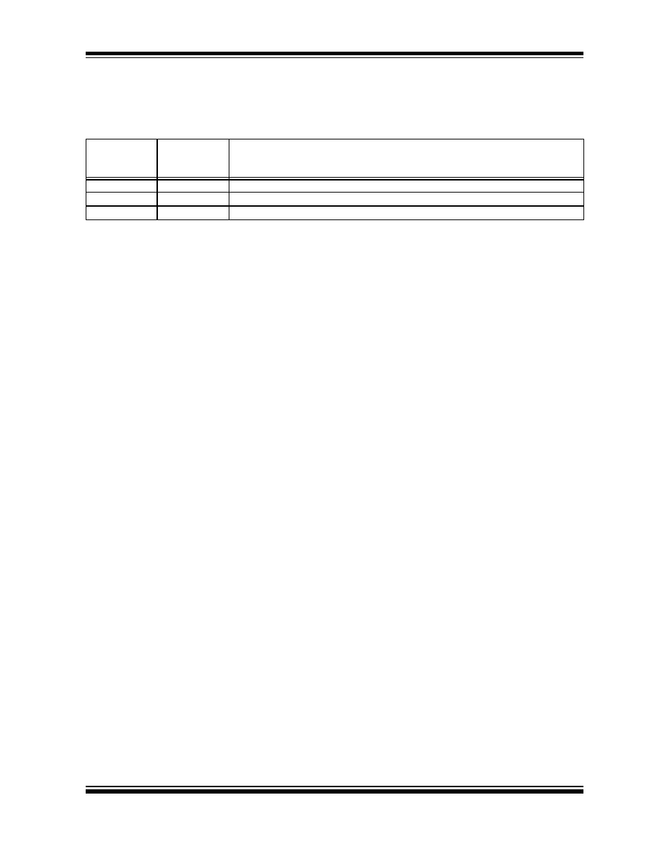
PIN DESCRIPTIONS
The descriptions for the pins are listed in Table 2-1.
TABLE 2-1:
PIN FUNCTION TABLE
Pin No.
(3-Pin SOT-223)
(3-Pin DDPAK)
Symbol
Description
1
GND
Connect this pin to the circuit ground.
2
V
OUT
Regulated output voltage.
3
V
IN
Unregulated Input voltage.

TC2117
DS21665B-page 4
©
2002 Microchip Technology Inc.
3.0
DETAILED DESCRIPTION
The TC2117 is a precision, positive output LDO. Unlike
bipolar regulators, the TC2117 supply current does not
increase proportionally with load current. In addition,
V
OUT
remains stable and within regulation over the
entire 0mA to 800mA operating load range.
FIGURE 3-1:
TYPICAL APPLICATION
CIRCUIT
3.1
Output Capacitor
A 1
µ
F (min) capacitor from V
OUT
to ground is required.
The output capacitor should have an effective series
resistance of 0.2
to 10
. A 1
µ
F capacitor should be
connected from V
IN
to GND if there is more than 10
inches of wire between the regulator and the AC filter
capacitor, or if a battery is used as the power source.
Aluminum electrolytic or tantalum capacitor types can
be used. (Since many aluminum electrolytic capacitors
freeze at approximately -30∞C, solid tantalums are rec-
ommended for applications operating below -25∞C.)
When operating from sources other than batteries, sup-
ply noise rejection and transient response can be
improved by increasing the value of the input and output
capacitors and employing passive filtering techniques.
3.2
Thermal Considerations
3.2.1
THERMAL SHUTDOWN
Integrated thermal protection circuitry shuts the regula-
tor off when die temperature exceeds 160∞C. The reg-
ulator remains off until the die temperature drops to
approximately 150∞C.
3.2.2
POWER DISSIPATION
The amount of power the regulator dissipates is prima-
rily a function of input and output voltage, and output
current. The following equation is used to calculate
worst case actual power dissipation:
EQUATION 3-1:
The
maximum
allowable
power
dissipation
(Equation 3-2) is a function of the maximum ambient
temperature (T
A
MAX
), the maximum allowable die tem-
perature (125∞C) and the thermal resistance from
junction-to-air (
JA
).
EQUATION 3-2:
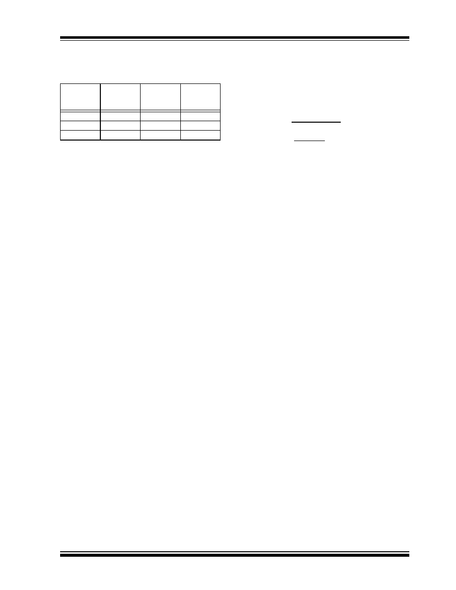
Table 3-1 shows various values of
JA
for the TC2117
mounted on a 1/16 inch, 2-layer PCB with 1 oz. copper
foil.
TABLE 3-1:
THERMAL RESISTANCE
GUIDELINES FOR TC2117 IN
3-PIN SOT-223 PACKAGE
C1
1
µF
Battery
TC2117
V
IN
V
OUT
C2
1
µF
GND
V
OUT
Copper
Area
(Topside)*
Copper
Area
(Backside)
Board Area
Thermal
Resistance
2500 sq mm
2500 sq mm
2500 sq mm
45∞C/W
1000 sq mm
2500 sq mm
2500 sq mm
45∞C/W
225 sq mm
2500 sq mm
2500 sq mm
53∞C/W
100 sq mm
2500 sq mm
2500 sq mm
59∞C/W
1000 sq mm
1000 sq mm
1000 sq mm
52∞C/W
1000 sq mm
0 sq mm
1000 sq mm
55∞C/W
*Tab of device attached to topside copper.
P
D
(V
IN
MAX
≠ V
OUT
MIN
)I
LOAD
MAX
Where:
P
D
= Worst case actual power dissipation
V
IN
MAX
= Maximum voltage on V
IN
V
OUT
MIN
= Maximum regulator output voltage
I
LOAD
MAX
= Maximum output (load) current
P
D
MAX
=
T
J
MAX
≠ T
A
MAX
JA
Where all terms are previously defined.
©
2002 Microchip Technology Inc.
DS21665B-page 5
TC2117
TABLE 3-2:
THERMAL RESISTANCE
GUIDELINES FOR TC2117 IN
3-PIN DDPAK PACKAGE
Equation 3-1
can
be
used
in
conjunction
with
Equation 3-2 to ensure regulator thermal operation is
within limits. For example:
Find:
1. Actual power dissipation
2. Maximum allowable dissipation
Actual power dissipation:
Maximum allowable power dissipation:
In this example, the TC2117 dissipates a maximum of
only 786mW; below the allowable limit of 1.186mW. In
a similar manner, Equation 3-1 and Equation 3-2 can
be used to calculate maximum current and/or input
voltage limits.
Copper
Area
(Topside)*
Copper
Area
(Backside)
Board Area
Thermal
Resistance
(
JA
)
2500 sq mm
2500 sq mm
2500 sq mm
25∞C/W
1000 sq mm
2500 sq mm
2500 sq mm
27∞C/W
125 sq mm
2500 sq mm
2500 sq mm
35∞C/W
*Tab of device attached to topside copper.
Given:
V
IN
MAX
=
5.0V ± 5%
V
OUT
MIN
=
3.3V ± 0.5%
I
LOADMAX
=
400mA
T
J
MAX
=
125∞C
T
A
MAX
=
55∞C
JA
=
59∞C/W (SOT-223)
P
D
(V
IN
MAX
≠ V
OUT
MIN
)I
LOAD
MAX
= [(5.0 x 1.05) ≠ (3.3 x .995)] 400 x 10
-3
= 786mW
P
D
MAX
=
(T
J
MAX
≠ T
A
MAX
)
JA
=
(125 ≠ 55)
59
=
1.186mW