 | –≠–ª–µ–∫—Ç—Ä–æ–Ω–Ω—ã–π –∫–æ–º–ø–æ–Ω–µ–Ω—Ç: TC4451 | –°–∫–∞—á–∞—Ç—å:  PDF PDF  ZIP ZIP |

© 2006 Microchip Technology Inc.
DS21987A-page 1
TC4451/TC4452
Features
∑ High Peak Output Current: 13A (typ.)
∑ Low Shoot-Through/Cross-Conduction Current in
Output Stage
∑ Wide Input Supply Voltage Operating Range:
- 4.5V to 18V
∑ High Continuous Output Current: 2.6A (max.)
∑ Matched Fast Rise and Fall Times:
- 21 ns with 10,000 pF Load
- 42 ns with 22,000 pF Load
∑ Matched Short Propagation Delays: 44 ns (typ.)
∑ Low Supply Current:
- With Logic `
1
' Input ≠ 140 A (typ.)
- With Logic `
0
' Input ≠ 40 A (typ.)
∑ Low Output Impedance: 0.9
(typ.)
∑ Latch-Up Protected: Will Withstand 1.5A Output
Reverse Current
∑ Input Will Withstand Negative Inputs Up To 5V
∑ Pin-Compatible with the TC4420/TC4429,
TC4421/TC4422 and TC4421A/TC4422A
MOSFET Drivers
∑ Space-Saving, Thermally-Enhanced, 8-Pin DFN
Package
Applications
∑ Line Drivers for Extra Heavily-Loaded Lines
∑ Pulse Generators
∑ Driving the Largest MOSFETs and IGBTs
∑ Local Power ON/OFF Switch
∑ Motor and Solenoid Driver
∑ LF Initiator
General Description
The TC4451/TC4452 are single-output MOSFET
drivers. These devices are high-current buffer/drivers
capable of driving large MOSFETs and Insulated Gate
Bipolar Transistors (IGBTs). The TC4451/TC4452 have
matched output rise and fall times, as well as matched
leading and falling-edge propagation delay times. The
TC4451/TC4452 devices also have very low cross-
conduction current, reducing the overall power
dissipation of the device.
These devices are essentially immune to any form of
upset, except direct overvoltage or over-dissipation.
They cannot be latched under any conditions within
their power and voltage ratings. These parts are not
subject to damage or improper operation when up to
5V of ground bounce is present on their ground
terminals. They can accept, without damage or logic
upset, more than 1.5A inductive current of either
polarity being forced back into their outputs. In addition,
all terminals are fully protected against up to 4 kV of
electrostatic discharge.
The TC4451/TC4452 inputs may be driven directly
from either TTL or CMOS (3V to 18V). In addition,
300 mV of hysteresis is built into the input, providing
noise immunity and allowing the device to be driven
from slowly rising or falling waveforms.
With both surface-mount and pin-through-hole
packages, in addition to a wide operating temperature
range, the TC4451/TC4452 family of 12A MOSFET
drivers fit into most any application where high gate/line
capacitance drive is required.
12A High-Speed MOSFET Drivers

TC4451/TC4452
DS21987A-page 2
© 2006 Microchip Technology Inc.
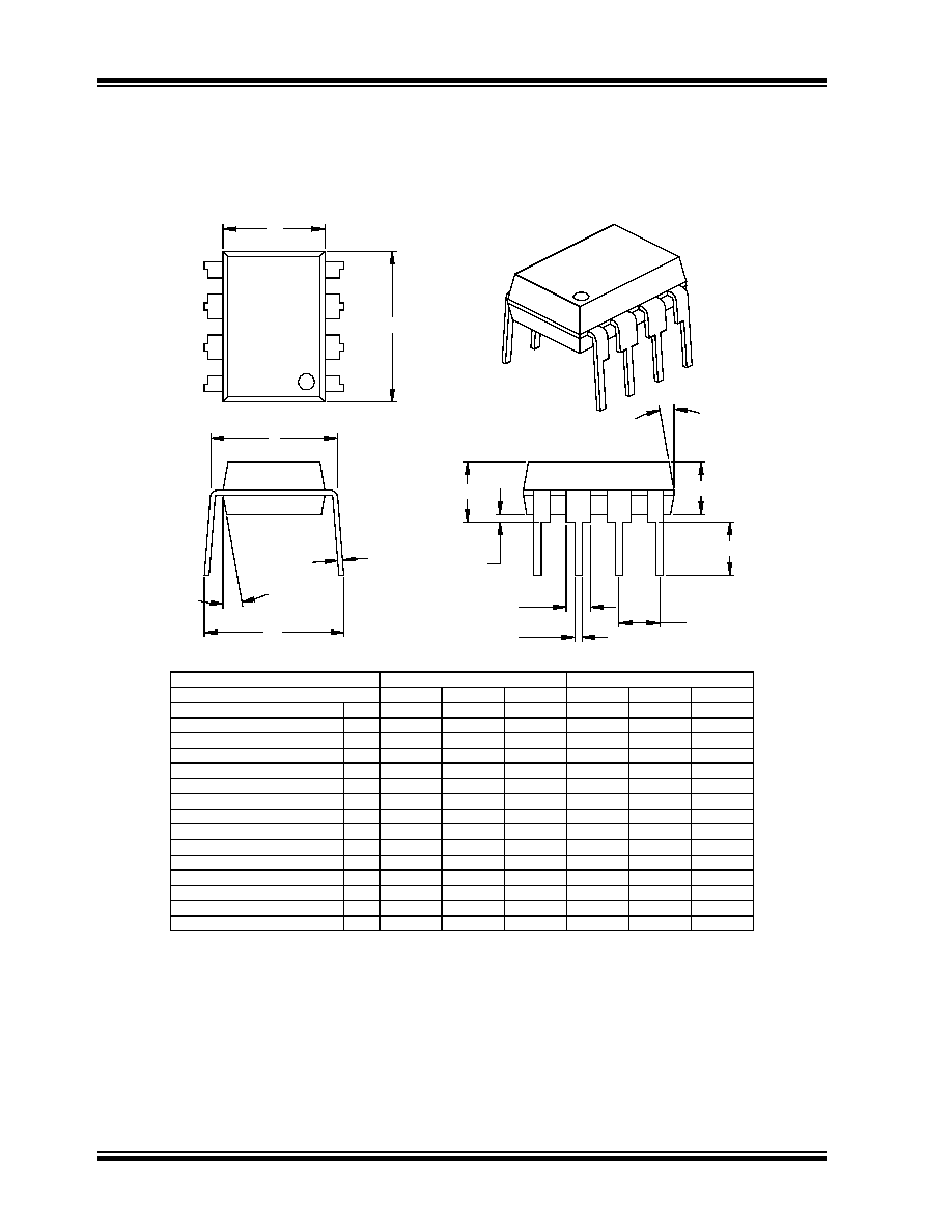
Package Types
(1)
Functional Block Diagram
8-Pin
1
2
3
4
V
DD
5
6
7
8
OUTPUT
GND
V
DD
INPUT
NC
GND
OUTPUT
TC4451
TC4452
5-Pin TO-220
V
DD
GND
IN
P
U
T
GN
D
OUTP
UT
TC4451
TC4452
Tab is
Common
to V
DD
Note 1: Duplicate pins must both be connected for proper operation.
2: Exposed pad of the DFN package is electrically isolated.
TC4451 TC4452
V
DD
OUTPUT
GND
OUTPUT
PDIP/SOIC
8-Pin DFN
(2)
V
DD
INPUT
NC
GND
2
3
4
5
6
7
8
1
TC4451
TC4452
V
DD
OUTPUT
GND
OUTPUT
TC4451 TC4452
V
DD
OUTPUT
GND
OUTPUT
Effective
Input
Output
Input
GND
V
DD
300 mV
4.7V
TC4451
C = 25 pF
TC4452
Inverting
Non-Inverting
140 A
Cross-Conduction
Reduction and Pre-Drive
Circuitry
Output

© 2006 Microchip Technology Inc.
DS21987A-page 3
TC4451/TC4452
1.0
ELECTRICAL
CHARACTERISTICS
Absolute Maximum Ratings
Supply Voltage .....................................................+20V
Input Voltage .................... (V
DD
+ 0.3V) to (GND ≠ 5V)
Input Current (V
IN
> V
DD
)................................... 50 mA
Stresses above those listed under "Absolute Maximum
Ratings" may cause permanent damage to the device. These
are stress ratings only and functional operation of the device
at these or any other conditions above those indicated in the
operation sections of the specifications is not implied.
Exposure to Absolute Maximum Rating conditions for
extended periods may affect device reliability.
DC CHARACTERISTICS
Electrical Specifications: Unless otherwise noted, T
A
= +25∞C with 4.5V
V
DD
18V.
Parameters
Sym
Min
Typ
Max
Units
Conditions
Input
Logic `
1
', High Input Voltage
V
IH
2.4
1.5
--
V
Logic `
0
', Low Input Voltage
V
IL
--
1.3
0.8
V
Input Current
I
IN
≠10
--
+10
A
0V
V
IN
V
DD
Input Voltage
V
IN
≠5
--
V
DD
+ 0.3
V
Output
High Output Voltage
V
OH
V
DD
≠ 0.025
--
--
V
DC Test
Low Output Voltage
V
OL
--
--
0.025
V
DC Test
Output Resistance, High
R
OH
--
1.0
1.5
I
OUT
= 10 mA, V
DD
= 18V
Output Resistance, Low
R
OL
--
0.9
1.5
I
OUT
= 10 mA, V
DD
= 18V
Peak Output Current
I
PK
--
13
--
A
V
DD
= 18V
Continuous Output Current
I
DC
2.6
--
--
A
10V
V
DD
18V (Note 2, Note 3)
Latch-Up Protection
Withstand Reverse Current
I
REV
--
>1.5
--
A
Duty cycle
2%, t
300 s
Switching Time (Note 1)
Rise Time
t
R
--
30
40
ns
Figure 4-1, C
L
= 15,000 pF
Fall Time
t
F
--
32
40
ns
Figure 4-1, C
L
= 15,000 pF
Propagation Delay Time
t
D1
--
44
52
ns
Figure 4-1, C
L
= 15,000 pF
Propagation Delay Time
t
D2
--
44
52
ns
Figure 4-1, C
L
= 15,000 pF
Power Supply
Power Supply Current
I
S
--
140
200
A
V
IN
= 3V
--
40
100
A
V
IN
= 0V
Operating Input Voltage
V
DD
4.5
--
18.0
V
Note 1:
Switching times ensured by design.
2:
Tested during characterization, not production tested.
3: Valid for AT and MF packages only. T
A
= +25∞C.

TC4451/TC4452
DS21987A-page 4
© 2006 Microchip Technology Inc.
DC CHARACTERISTICS (OVER OPERATING TEMPERATURE RANGE)
TEMPERATURE CHARACTERISTICS
Electrical Specifications: Unless otherwise noted, over operating temperature range with 4.5V
V
DD
18V.
Parameters
Sym
Min
Typ
Max
Units
Conditions
Input
Logic `
1
', High Input Voltage
V
IH
2.4
--
--
V
Logic `
0
', Low Input Voltage
V
IL
--
--
0.8
V
Input Current
I
IN
≠10
--
+10
A
0V
V
IN
V
DD
Output
High Output Voltage
V
OH
V
DD
≠ 0.025
--
--
V
DC Test
Low Output Voltage
V
OL
--
--
0.025
V
DC Test
Output Resistance, High
R
OH
--
--
2.2
I
OUT
= 10 mA, V
DD
= 18V
Output Resistance, Low
R
OL
--
--
2.0
I
OUT
= 10 mA, V
DD
= 18V
Switching Time (Note 1)
Rise Time
t
R
--
35
60
ns
Figure 4-1, C
L
= 15,000 pF
Fall Time
t
F
--
38
60
ns
Figure 4-1, C
L
= 15,000 pF
Propagation Delay Time
t
D1
--
55
65
ns
Figure 4-1, C
L
= 15,000 pF
Propagation Delay Time
t
D2
--
55
65
ns
Figure 4-1, C
L
= 15,000 pF
Power Supply
Power Supply Current
I
S
--
200
400
A
V
IN
= 3V
--
50
150
A
V
IN
= 0V
Operating Input Voltage
V
DD
4.5
--
18.0
V
Note 1:
Switching times ensured by design.
Electrical Specifications: Unless otherwise noted, all parameters apply with 4.5V
V
DD
18V.
Parameters
Sym
Min
Typ
Max
Units
Conditions
Temperature Ranges
Specified Temperature Range (V)
T
A
≠40
--
+125
∞C
Maximum Junction Temperature
T
J
--
--
+150
∞C
Storage Temperature Range
T
A
≠65
--
+150
∞C
Package Thermal Resistances
Thermal Resistance, 5L-TO-220
JA
--
71
--
∞C/W
Without heat sink
Thermal Resistance, 8L-6x5 DFN
JA
--
33.2
--
∞C/W
Typical 4-layer board with
vias to ground plane
Thermal Resistance, 8L-PDIP
JA
--
125
--
∞C/W
Thermal Resistance, 8L-SOIC
JA
--
155
--
∞C/W
© 2006 Microchip Technology Inc.
DS21987A-page 5
TC4451/TC4452
2.0
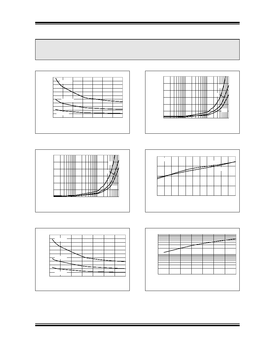
TYPICAL PERFORMANCE CURVES
Note: Unless otherwise indicated, T
A
= +25∞C with 4.5V
V
DD
18V.
FIGURE 2-1:
Rise Time vs. Supply
Voltage.
FIGURE 2-2:
Rise Time vs. Capacitive
Load.
FIGURE 2-3:
Fall Time vs. Supply
Voltage.
FIGURE 2-4:
Fall Time vs. Capacitive
Load.
FIGURE 2-5:
Rise and Fall Times vs.
Temperature.
FIGURE 2-6:
Crossover Energy vs.
Supply Voltage.
Note:
The graphs and tables provided following this note are a statistical summary based on a limited number of
samples and are provided for informational purposes only. The performance characteristics listed herein
are not tested or guaranteed. In some graphs or tables, the data presented may be outside the specified
operating range (e.g., outside specified power supply range) and therefore outside the warranted range.
0
20
40
60
80
100
120
140
160
180
200
220
4
6
8
10
12
14
16
18
Supply Voltage (V)
R
i
se
Tim
e
(
n
s)
47,000 pF
22,000 pF
10,000 pF
0
50
100
150
200
250
300
100
1000
10000
100000
Capacitive Load (pF)
Ri
s
e
T
i
m
e
(
n
s
)
5V
18V
10V
0
20
40
60
80
100
120
140
160
180
200
220
4
6
8
10
12
14
16
18
Supply Voltage (V)
Fall Time (ns)
47,000 pF
22,000 pF
10,000 pF
0
50
100
150
200
250
300
100
1000
10000
100000
Capacitive Load (pF)
Fal
l
Ti
m
e
(
n
s)
5V
18V
10V
0
10
20
30
40
-40 -25 -10
5
20
35
50
65
80
95 110 125
Temperature (∞C)
R
i
se and Fal
l
Ti
mes (
n
s)
t
RISE
t
FALL
V
DD
= 18V
1E-09
1E-08
1E-07
4
6
8
10
12
14
16
18
Supply Voltage (V)
Crossover Energy (
A
∑
sec)
10
-7
10
-8
10
-9

TC4451/TC4452
DS21987A-page 6
© 2006 Microchip Technology Inc.
Note: Unless otherwise indicated, T
A
= +25∞C with 4.5V
V
DD
18V.
FIGURE 2-7:
Propagation Delay vs.
Supply Voltage.
FIGURE 2-8:
Propagation Delay vs. Input
Amplitude.
FIGURE 2-9:
Propagation Delay vs.
Temperature.
FIGURE 2-10:
Quiescent Supply Current
vs. Supply Voltage.
FIGURE 2-11:
Quiescent Supply Current
vs. Temperature.
FIGURE 2-12:
Input Threshold vs.
Temperature.
40
45
50
55
60
65
70
75
80
85
90
95
4
6
8
10
12
14
16
18
Supply Voltage (V)
P
r
op
ag
at
i
o
n D
e
l
a
y (
n
s)
t
D2
t
D1
C
LOAD
= 15,000 pF
V
IN
= 5V
40
45
50
55
60
65
70
75
80
85
90
95
100
2
3
4
5
6
7
8
9
10
Input Amplitude (V)
P
r
o
p
aga
t
ion
D
e
la
y
(
n
s)
t
D2
t
D1
C
LOAD
= 15,000 pF
V
DD
= 10V
30
35
40
45
50
55
60
-40 -25 -10
5
20 35 50 65 80 95 110 125
Temperature (
o
C)
P
r
o
p
aga
t
io
n D
e
l
ay
(
n
s)
t
D2
t
D1
V
DD
= 10V
V
IN
= 5V
C
LOAD
= 15,000 pF
20
40
60
80
100
120
140
4
6
8
10
12
14
16
18
Supply Voltage (V)
I
Q
U
I
ESCEN
T
(
A)
INPUT = High
INPUT = Low
20
40
60
80
100
120
140
160
180
200
220
-40 -25 -10 5
20 35 50 65 80 95 110 125
Temperature (
o
C)
I
Q
U
IESC
ENT
(
A)
INPUT = High
V
DD
= 18 V
INPUT = Low
1
1.1
1.2
1.3
1.4
1.5
1.6
1.7
1.8
1.9
2
-40 -25 -10 5
20 35 50 65 80 95 110 125
Temperature (
o
C)
I
n
put
Th
re
sho
l
d (
V
)
V
IH
V
IL
V
DD
= 12 V

© 2006 Microchip Technology Inc.
DS21987A-page 7
TC4451/TC4452
Note: Unless otherwise indicated, T
A
= +25∞C with 4.5V
V
DD
18V.
FIGURE 2-13:
Input Threshold vs. Supply
Voltage.
FIGURE 2-14:
High-State Output
Resistance vs. Supply Voltage.
FIGURE 2-15:
Low-State Output
Resistance vs. Supply Voltage.
FIGURE 2-16:
Supply Current vs.
Capacitive Load (V
DD
= 18V).
FIGURE 2-17:
Supply Current vs.
Capacitive Load (V
DD
= 12V).
FIGURE 2-18:
Supply Current vs.
Capacitive Load (V
DD
= 6V).
1
1.1
1.2
1.3
1.4
1.5
1.6
1.7
1.8
1.9
2
4
6
8
10
12
14
16
18
Supply Voltage (V)
I
n
p
u
t Thr
esh
ol
d
(V
)
V
IH
V
IL
0.0
0.5
1.0
1.5
2.0
2.5
3.0
3.5
4.0
4
6
8
10
12
14
16
18
Supply Voltage (V)
R
OUT
-
HI
(
)
T
J
= 125
o
C
T
J
= 25
o
C
V
IN
= 5V (TC4452)
V
IN
= 0V (TC4451)
0.0
0.5
1.0
1.5
2.0
2.5
3.0
4
6
8
10
12
14
16
18
Supply Voltage (V)
R
O
U
T-
LO
(
)
T
J
= 125
o
C
T
J
= 25
o
C
V
IN
= 0V (TC4452)
V
IN
= 5V (TC4451)
0
50
100
150
200
250
300
100
1,000
10,000
100,000
Capacitive Load (pF)
S
u
ppl
y C
u
r
r
e
n
t
(m
A
)
V
DD
= 18 V
2 MHz
1 MHz
200 kHz
100 kHz
50 kHz
10 kHz
0
50
100
150
200
250
300
100
1,000
10,000
100,000
Capacitive Load (pF)
S
u
ppl
y C
u
r
r
e
n
t
(m
A
)
V
DD
= 12 V
2 MHz
1 MHz
200 kHz
100 kHz
50 kHz
10 kHz
-5
15
35
55
75
95
115
135
155
175
100
1,000
10,000
100,000
Capacitive Load (pF)
Su
p
p
ly
Cu
r
r
e
n
t
(
m
A)
V
DD
= 6 V
2 MHz
1 MHz
200 kHz
100 kHz
50 kHz
10 kHz

TC4451/TC4452
DS21987A-page 8
© 2006 Microchip Technology Inc.
Note: Unless otherwise indicated, T
A
= +25∞C with 4.5V
V
DD
18V.
FIGURE 2-19:
Supply Current vs.
Frequency (V
DD
= 18V).
FIGURE 2-20:
Supply Current vs.
Frequency (V
DD
= 12V).
FIGURE 2-21:
Supply Current vs.
Frequency (V
DD
= 6V).
0
50
100
150
200
250
10
100
1000
10000
Frequency (kHz)
Suppl
y C
u
r
r
e
nt (mA
)
V
DD
= 18 V
0.1 F
47,000 pF
22,000 pF
15,000 pF
10,000 pF
1,000 pF
470 pF
0
50
100
150
200
250
10
100
1000
10000
Frequency (kHz)
S
u
ppl
y C
u
r
r
e
n
t
(m
A
)
V
DD
= 12 V
0.1 F
47,000 pF
22,000 pF
15,000 pF
10,000 pF
1,000 pF
470 pF
0
50
100
150
200
250
10
100
1000
10000
Frequency (kHz)
S
u
ppl
y C
u
r
r
e
n
t
(m
A
)
V
DD
= 6 V
0.1 F
47,000 pF
22,000 pF
15,000 pF
10,000 pF
1,000 pF
470 pF

© 2006 Microchip Technology Inc.
DS21987A-page 9
TC4451/TC4452
3.0
PIN DESCRIPTIONS
The descriptions of the pins are listed in Table 3-1.
TABLE 3-1:
PIN FUNCTION TABLE
3.1
Supply Input (V
DD
)
The V
DD
input is the bias supply for the MOSFET driver
and is rated for 4.5V to 18V with respect to the ground
pin. The V
DD
input should be bypassed to ground with
a local ceramic capacitor. The value of the capacitor
should be chosen based on the capacitive load that is
being driven. A minimum value of 1.0 F is suggested.
3.2
Control Input
The MOSFET driver input is a high-impedance,
TTL/CMOS-compatible input. The input also has
300 mV of hysteresis between the high and low
thresholds that prevents output glitching even when the
rise and fall time of the input signal is very slow.
3.3
CMOS Push-Pull Output
The MOSFET driver output is a low-impedance,
CMOS, push-pull style output capable of driving a
capacitive load with 12A peak currents. The MOSFET
driver output is capable of withstanding 1.5A peak
reverse currents of either polarity.
3.4
Ground
The ground pins are the return path for the bias current
and for the high peak currents that discharge the load
capacitor. The ground pins should be tied into a ground
plane or have very short traces to the bias supply
source return.
3.5
Exposed Metal Pad
The exposed metal pad of the 6x5 DFN package is not
internally connected to any potential. Therefore, this
pad can be connected to a ground plane or other
copper plane on a Printed Circuit Board (PCB) to aid in
heat removal from the package.
3.6
Metal Tab
The metal tab of the TO-220 package is connected to
the V
DD
potential of the device. This connection to V
DD
can be used as a current carrying path for the device.
Pin No.
8-Pin PDIP,
SOIC
Pin No.
8-Pin DFN
Pin No.
5-Pin TO-220
Symbol
Description
1
1
--
V
DD
Supply input, 4.5V to 18V
2
2
1
INPUT
Control input, TTL/CMOS-compatible input
3
3
--
NC
No connection
4
4
2
GND
Ground
5
5
4
GND
Ground
6
6
5
OUTPUT
CMOS push-pull output
7
7
--
OUTPUT
CMOS push-pull output
8
8
3
V
DD
Supply input, 4.5V to 18V
--
PAD
--
NC
Exposed metal pad
--
--
TAB
V
DD
Metal tab is at the V
DD
potential

TC4451/TC4452
DS21987A-page 10
© 2006 Microchip Technology Inc.
4.0
APPLICATIONS INFORMATION
FIGURE 4-1:
Switching Time Test Circuits.
Inverting Driver
Non-Inverting Driver
Input
t
D1
tF
t
R
t
D2
Input: 100 kHz,
square wave,
t
RISE
= t
FALL
10 ns
Output
Input
Output
t
D1
t
F
t
R
t
D2
+5V
10%
90%
10%
90%
10%
90%
+18V
0V
90%
10%
10%
10%
90%
+5V
+18V
0V
0V
0V
90%
2
6
7
5
4
1
8
C
L
= 15,000 pF
0.1 F
4.7 F
Input
V
DD
= 18V
Output
0.1 F
TC4451
TC4452
Note: Pinout shown is for the DFN, PDIP and SOIC packages.
V
DD
V
DD
Input
GND
GND
Output
Output

© 2006 Microchip Technology Inc.
DS21987A-page 11
TC4451/TC4452
5.0
PACKAGING INFORMATION
5.1
Package Marking Information
XXXXXXXX
XXXXXNNN
YYWW
8-Lead PDIP (300 mil)
Example:
TC4451V
PA^^ 256
0649
5-Lead TO-220
XXXXXXXXX
XXXXXXXXX
YYWWNNN
Example:
TC4451
XXXXXXXXX
0649256
VAT
^^
Legend: XX...X
Customer-specific information
Y
Year code (last digit of calendar year)
YY
Year code (last 2 digits of calendar year)
WW
Week code (week of January 1 is week `01')
NNN
Alphanumeric traceability code
Pb-free JEDEC designator for Matte Tin (Sn)
*
This package is Pb-free. The Pb-free JEDEC designator ( )
can be found on the outer packaging for this package.
Note:
In the event the full Microchip part number cannot be marked on one line, it will
be carried over to the next line, thus limiting the number of available
characters for customer-specific information.
3
e
3
e
8-Lead DFN-S
Example
:
TC4451
VMF
^
0649
256
8-Lead SOIC (150 mil)
Example
:
XXXXXXXX
XXXXYYWW
NNN
TC4451V
OA ^^ 0649
256
3
e
3
e
3
e
3
e
XXXXXXX
XXXXXXX
XXYYWW
NNN

TC4451/TC4452
DS21987A-page 12
© 2006 Microchip Technology Inc.
5-Lead Plastic Transistor Outline (AT) (TO-220)
L
H1
Q
E
e1
e
C1
J1
F
A
D
(5∞)
ÿP
EJECTOR PIN
e3
Drawing No. C04-036
Notes:
Dimensions D and E1 do not include mold flash or protrusions. Mold flash or protrusions shall not exceed .010" (0.254 mm) per side.
JEDEC equivalent: TO-220
* Controlling Parameter
Mold Draft Angle
Lead Width
Lead Thickness
C1
.014
Dimension Limits
Overall Height
Lead Length
Overall Width
Lead Pitch
A
L
E
.540
MIN
e
Units
.060
INCHES*
.022
0.36
0.56
MILLIMETERS
.190
.560
13.72
MIN
MAX
4.83
14.22
MAX
.160
4.06
3∞
7∞
3∞
7∞
Overall Length
D
1.02
0.64
.040
.025
Overall Lead Centers
e1
.263
.385
.560
.273
6.68
6.93
.072
1.52
1.83
.415
9.78
10.54
.590
14.22
14.99
Through Hole Diameter
P
.146
.156
3.71
3.96
J1
Base to Bottom of Lead
.090
2.29
.115
2.92
Through Hole Center
Q
.103
2.87
.113
2.62
Flag Thickness
F
.045
1.40
.055
1.14
Flag Length
H1
.234
6.55
.258
5.94
Space Between Leads
e3
.030
1.02
.040
0.76
Revised 08-01-05

© 2006 Microchip Technology Inc.
DS21987A-page 13
TC4451/TC4452
8-Lead Plastic Dual Flat No Lead Package (MF) 6x5 mm Body (DFN-S) ≠ Saw Singulated
TC4451/TC4452
DS21987A-page 14
© 2006 Microchip Technology Inc.
8-Lead Plastic Dual In-line (PA) ≠ 300 mil (PDIP)
B1
B
A1
A
L
A2
p
E
eB
c
E1
n
D
1
2
Units
INCHES*
MILLIMETERS
Dimension Limits
MIN
NOM
MAX
MIN
NOM
MAX
Number of Pins
n
8
8
Pitch
p
.100
2.54
Top to Seating Plane
A
.140
.155
.170
3.56
3.94
4.32
Molded Package Thickness
A2
.115
.130
.145
2.92
3.30
3.68
Base to Seating Plane
A1
.015
0.38
Shoulder to Shoulder Width
E
.300
.313
.325
7.62
7.94
8.26
Molded Package Width
E1
.240
.250
.260
6.10
6.35
6.60
Overall Length
D
.360
.373
.385
9.14
9.46
9.78
Tip to Seating Plane
L
.125
.130
.135
3.18
3.30
3.43
Lead Thickness
c
.008
.012
.015
0.20
0.29
0.38
Upper Lead Width
B1
.045
.058
.070
1.14
1.46
1.78
Lower Lead Width
B
.014
.018
.022
0.36
0.46
0.56
Overall Row Spacing
ß
eB
.310
.370
.430
7.87
9.40
10.92
Mold Draft Angle Top
5
10
15
5
10
15
Mold Draft Angle Bottom
5
10
15
5
10
15
* Controlling Parameter
Notes:
Dimensions D and E1 do not include mold flash or protrusions. Mold flash or protrusions shall not exceed
JEDEC Equivalent: MS-001
Drawing No. C04-018
.010" (0.254mm) per side.
ß Significant Characteristic

© 2006 Microchip Technology Inc.
DS21987A-page 15
TC4451/TC4452
8-Lead Plastic Small Outline (OA) ≠ Narrow, 150 mil (SOIC)
Foot Angle
0
4
8
0
4
8
15
12
0
15
12
0
Mold Draft Angle Bottom
15
12
0
15
12
0
Mold Draft Angle Top
0.51
0.42
0.33
.020
.017
.013
B
Lead Width
0.25
0.23
0.20
.010
.009
.008
c
Lead Thickness
0.76
0.62
0.48
.030
.025
.019
L
Foot Length
0.51
0.38
0.25
.020
.015
.010
h
Chamfer Distance
5.00
4.90
4.80
.197
.193
.189
D
Overall Length
3.99
3.91
3.71
.157
.154
.146
E1
Molded Package Width
6.20
6.02
5.79
.244
.237
.228
E
Overall Width
0.25
0.18
0.10
.010
.007
.004
A1
Standoff ß
1.55
1.42
1.32
.061
.056
.052
A2
Molded Package Thickness
1.75
1.55
1.35
.069
.061
.053
A
Overall Height
1.27
.050
p
Pitch
8
8
n
Number of Pins
MAX
NOM
MIN
MAX
NOM
MIN
Dimension Limits
MILLIMETERS
INCHES*
Units
2
1
D
n
p
B
E
E1
h
L
c
45
∞
A2
A
A1
* Controlling Parameter
Notes:
Dimensions D and E1 do not include mold flash or protrusions. Mold flash or protrusions shall not exceed
.010" (0.254mm) per side.
JEDEC Equivalent: MS-012
Drawing No. C04-057
ß Significant Characteristic

TC4451/TC4452
DS21987A-page 16
© 2006 Microchip Technology Inc.
NOTES:

© 2006 Microchip Technology Inc.
DS21987A-page 17
TC4451/TC4452
APPENDIX A: REVISION HISTORY
Revision A (February 2006)
∑ Original Release of this Document.

TC4451/TC4452
DS21987A-page 18
© 2006 Microchip Technology Inc.
NOTES:
© 2006 Microchip Technology Inc.
DS21987A-page 19
TC4451/TC4452
PRODUCT IDENTIFICATION SYSTEM
To order or obtain information, e.g., on pricing or delivery, refer to the factory or the listed sales office
.
Device:
TC4451: 12A High-Speed MOSFET Driver, Inverting
TC4452: 12A High-Speed MOSFET Driver, Non-Inverting
Temperature Range:
V
= -40∞C to +125∞C
Package: *
AT
= TO-220, 5-lead
MF
= Dual, Flat, No-Lead (6x5 mm Body), 8-lead
MF713 = Dual, Flat, No-Lead (6x5 mm Body), 8-lead
(Tape and Reel)
PA
= Plastic DIP (300 mil Body), 8-lead
OA
= Plastic SOIC (150 mil Body), 8-lead
OA713 = Plastic SOIC (150 mil Body), 8-lead
(Tape and Reel)
*All package offerings are Pb Free (Lead Free).
PART NO.
X
XX
Package
Temperature
Range
Device
Examples:
a)
TC4451VAT:
12A High-Speed Inverting
MOSFET Driver,
TO-220 package
b)
TC4451VOA:
12A High-Speed Inverting
MOSFET Driver,
SOIC package
c)
TC4451VMF:
12A High-Speed Inverting
MOSFET Driver,
DFN package
a)
TC4452VPA:
12A High-Speed
Non-Inverting MOSFET
Driver, PDIP package
b)
TC4452VOA: 12A High-Speed
Non-Inverting
MOSFET Driver,
SOIC package
c)
TC4452VMF: 12A High-Speed
Non-Inverting MOSFET
Driver, DFN package
XXX
Tape & Reel

TC4451/TC4452
DS21987A-page 20
© 2006 Microchip Technology Inc.
NOTES:

© 2006 Microchip Technology Inc.
DS21987A-page 21
Information contained in this publication regarding device
applications and the like is provided only for your convenience
and may be superseded by updates. It is your responsibility to
ensure that your application meets with your specifications.
MICROCHIP MAKES NO REPRESENTATIONS OR WAR-
RANTIES OF ANY KIND WHETHER EXPRESS OR IMPLIED,
WRITTEN OR ORAL, STATUTORY OR OTHERWISE,
RELATED TO THE INFORMATION, INCLUDING BUT NOT
LIMITED TO ITS CONDITION, QUALITY, PERFORMANCE,
MERCHANTABILITY OR FITNESS FOR PURPOSE.
Microchip disclaims all liability arising from this information and
its use. Use of Microchip devices in life support and/or safety
applications is entirely at the buyer's risk, and the buyer agrees
to defend, indemnify and hold harmless Microchip from any and
all damages, claims, suits, or expenses resulting from such
use. No licenses are conveyed, implicitly or otherwise, under
any Microchip intellectual property rights.
Trademarks
The Microchip name and logo, the Microchip logo, Accuron,
dsPIC, K
EE
L
OQ
, microID, MPLAB, PIC, PICmicro, PICSTART,
PRO MATE, PowerSmart, rfPIC, and SmartShunt are
registered trademarks of Microchip Technology Incorporated
in the U.S.A. and other countries.
AmpLab, FilterLab, Migratable Memory, MXDEV, MXLAB,
PICMASTER, SEEVAL, SmartSensor and The Embedded
Control Solutions Company are registered trademarks of
Microchip Technology Incorporated in the U.S.A.
Analog-for-the-Digital Age, Application Maestro, dsPICDEM,
dsPICDEM.net, dsPICworks, ECAN, ECONOMONITOR,
FanSense, FlexROM, fuzzyLAB, In-Circuit Serial
Programming, ICSP, ICEPIC, Linear Active Thermistor,
MPASM, MPLIB, MPLINK, MPSIM, PICkit, PICDEM,
PICDEM.net, PICLAB, PICtail, PowerCal, PowerInfo,
PowerMate, PowerTool, Real ICE, rfLAB, rfPICDEM, Select
Mode, Smart Serial, SmartTel, Total Endurance, UNI/O,
WiperLock and Zena are trademarks of Microchip Technology
Incorporated in the U.S.A. and other countries.
SQTP is a service mark of Microchip Technology Incorporated
in the U.S.A.
All other trademarks mentioned herein are property of their
respective companies.
© 2006, Microchip Technology Incorporated, Printed in the
U.S.A., All Rights Reserved.
Printed on recycled paper.
Note the following details of the code protection feature on Microchip devices:
∑
Microchip products meet the specification contained in their particular Microchip Data Sheet.
∑
Microchip believes that its family of products is one of the most secure families of its kind on the market today, when used in the
intended manner and under normal conditions.
∑
There are dishonest and possibly illegal methods used to breach the code protection feature. All of these methods, to our
knowledge, require using the Microchip products in a manner outside the operating specifications contained in Microchip's Data
Sheets. Most likely, the person doing so is engaged in theft of intellectual property.
∑
Microchip is willing to work with the customer who is concerned about the integrity of their code.
∑
Neither Microchip nor any other semiconductor manufacturer can guarantee the security of their code. Code protection does not
mean that we are guaranteeing the product as "unbreakable."
Code protection is constantly evolving. We at Microchip are committed to continuously improving the code protection features of our
products. Attempts to break Microchip's code protection feature may be a violation of the Digital Millennium Copyright Act. If such acts
allow unauthorized access to your software or other copyrighted work, you may have a right to sue for relief under that Act.
Microchip received ISO/TS-16949:2002 quality system certification for
its worldwide headquarters, design and wafer fabrication facilities in
Chandler and Tempe, Arizona and Mountain View, California in
October 2003. The Company's quality system processes and
procedures are for its PICmicro
Æ
8-bit MCUs, K
EE
L
OQ
Æ
code hopping
devices, Serial EEPROMs, microperipherals, nonvolatile memory and
analog products. In addition, Microchip's quality system for the design
and manufacture of development systems is ISO 9001:2000 certified.

DS21987A-page 22
© 2006 Microchip Technology Inc.
AMERICAS
Corporate Office
2355 West Chandler Blvd.
Chandler, AZ 85224-6199
Tel: 480-792-7200
Fax: 480-792-7277
Technical Support:
http://support.microchip.com
Web Address:
www.microchip.com
Atlanta
Alpharetta, GA
Tel: 770-640-0034
Fax: 770-640-0307
Boston
Westborough, MA
Tel: 774-760-0087
Fax: 774-760-0088
Chicago
Itasca, IL
Tel: 630-285-0071
Fax: 630-285-0075
Dallas
Addison, TX
Tel: 972-818-7423
Fax: 972-818-2924
Detroit
Farmington Hills, MI
Tel: 248-538-2250
Fax: 248-538-2260
Kokomo
Kokomo, IN
Tel: 765-864-8360
Fax: 765-864-8387
Los Angeles
Mission Viejo, CA
Tel: 949-462-9523
Fax: 949-462-9608
San Jose
Mountain View, CA
Tel: 650-215-1444
Fax: 650-961-0286
Toronto
Mississauga, Ontario,
Canada
Tel: 905-673-0699
Fax: 905-673-6509
ASIA/PACIFIC
Australia - Sydney
Tel: 61-2-9868-6733
Fax: 61-2-9868-6755
China - Beijing
Tel: 86-10-8528-2100
Fax: 86-10-8528-2104
China - Chengdu
Tel: 86-28-8676-6200
Fax: 86-28-8676-6599
China - Fuzhou
Tel: 86-591-8750-3506
Fax: 86-591-8750-3521
China - Hong Kong SAR
Tel: 852-2401-1200
Fax: 852-2401-3431
China - Qingdao
Tel: 86-532-8502-7355
Fax: 86-532-8502-7205
China - Shanghai
Tel: 86-21-5407-5533
Fax: 86-21-5407-5066
China - Shenyang
Tel: 86-24-2334-2829
Fax: 86-24-2334-2393
China - Shenzhen
Tel: 86-755-8203-2660
Fax: 86-755-8203-1760
China - Shunde
Tel: 86-757-2839-5507
Fax: 86-757-2839-5571
China - Wuhan
Tel: 86-27-5980-5300
Fax: 86-27-5980-5118
China - Xian
Tel: 86-29-8833-7250
Fax: 86-29-8833-7256
ASIA/PACIFIC
India - Bangalore
Tel: 91-80-2229-0061
Fax: 91-80-2229-0062
India - New Delhi
Tel: 91-11-5160-8631
Fax: 91-11-5160-8632
India - Pune
Tel: 91-20-2566-1512
Fax: 91-20-2566-1513
Japan - Yokohama
Tel: 81-45-471- 6166
Fax: 81-45-471-6122
Korea - Gumi
Tel: 82-54-473-4301
Fax: 82-54-473-4302
Korea - Seoul
Tel: 82-2-554-7200
Fax: 82-2-558-5932 or
82-2-558-5934
Malaysia - Penang
Tel: 60-4-646-8870
Fax: 60-4-646-5086
Philippines - Manila
Tel: 63-2-634-9065
Fax: 63-2-634-9069
Singapore
Tel: 65-6334-8870
Fax: 65-6334-8850
Taiwan - Hsin Chu
Tel: 886-3-572-9526
Fax: 886-3-572-6459
Taiwan - Kaohsiung
Tel: 886-7-536-4818
Fax: 886-7-536-4803
Taiwan - Taipei
Tel: 886-2-2500-6610
Fax: 886-2-2508-0102
Thailand - Bangkok
Tel: 66-2-694-1351
Fax: 66-2-694-1350
EUROPE
Austria - Wels
Tel: 43-7242-2244-399
Fax: 43-7242-2244-393
Denmark - Copenhagen
Tel: 45-4450-2828
Fax: 45-4485-2829
France - Paris
Tel: 33-1-69-53-63-20
Fax: 33-1-69-30-90-79
Germany - Munich
Tel: 49-89-627-144-0
Fax: 49-89-627-144-44
Italy - Milan
Tel: 39-0331-742611
Fax: 39-0331-466781
Netherlands - Drunen
Tel: 31-416-690399
Fax: 31-416-690340
Spain - Madrid
Tel: 34-91-708-08-90
Fax: 34-91-708-08-91
UK - Wokingham
Tel: 44-118-921-5869
Fax: 44-118-921-5820
W
ORLDWIDE
S
ALES
AND
S
ERVICE
10/31/05