TC55 Series
TC55-24 02/01/01
© 2001 Microchip Technology Inc. DS21435A
FEATURES
I
Very Low Dropout Voltage .... 120mV typ at 100mA
380mV typ at 200mA
I
High Output Current .............. 250mA (V
OUT
= 5.0V)
I
High Accuracy Output Voltage ........................
±
2%
(
±
1% Semicustom Version)
I
Wide Output Voltage Range .................... 1.1V-6.0V
I
Low Power Consumption ................... 1.1
µ
A (Typ.)
I
Low Temperature Drift ................
±
100ppm/
°
C (Typ.)
I
Excellent Line Regulation .................. 0.2%/V (Typ.)
I
Package Options ............................. 3-Pin SOT-23A
3-Pin SOT-89
I
Short Circuit Protection
I
Custom Voltages Available from 1.1V to 6.0V in
0.1V Steps for a 2%, and 2.0V to 6.0V for a 1%
Tolerance
APPLICATIONS
I
Battery-Powered Devices
I
Cameras and Portable Video Equipment
I
Pagers and Cellular Phones
I
Solar-Powered Instruments
I
Consumer Products
GENERAL DESCRIPTION
The TC55 Series is a collection of CMOS low dropout
positive voltage regulators which can source up to 250mA of
current with an extremely low input-output voltage differen-
tial of 380mV at 200mA.
The low dropout voltage combined with the low current
consumption of only 1.1
µ
A makes this part ideal for battery
operation. The low voltage differential (dropout voltage)
extends battery operating lifetime. It also permits high
currents in small packages when operated with minimum
V
IN
V
OUT
differentials.
The circuit also incorporates short-circuit protection to
ensure maximum reliability.
1
µ
A LOW DROPOUT POSITIVE VOLTAGE REGULATOR
Output Voltage:
Ex: 20 = 2.0V; 60 = 6.0V 1.0% Tol.
Ex: 11 = 1.1V; 60 = 6.0V 2.0% Tol.
Extra Feature Code: Fixed: 0
Tolerance:
1 = 1.0% (Custom)
2 = 2.0% (Standard)
Temperature: E: 40
°
C to +85
°
C
Package Type and Pin Count:
CB: 3-Pin SOT-23A
(equivalent to EIAJ SC-59)
MB: 3-Pin SOT-89
Taping Direction:
TR or 713: Standard Taping
RT or 723: Reverse Taping
PART CODE
TC55 RP XX X X X XX XXX
ORDERING INFORMATION
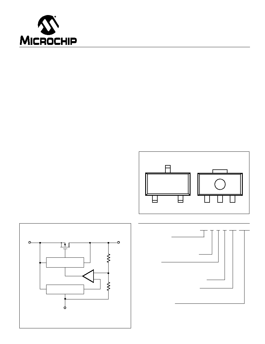
PIN CONFIGURATIONS
FUNCTIONAL BLOCK DIAGRAM
VIN
VOUT
GND
+
Short-circuit
Protection
Voltage
Reference
1
3
2
VIN
VOUT
GND
TC55
VIN
VOUT
GND
TC55
1
3
2
3-Pin SOT-23A
3-Pin SOT-89
*SOT-23A-3 is equivalent to EIAJ SC-59
TC55 Series
2
1
µ
A LOW DROPOUT POSITIVE VOLTAGE REGULATOR
© 2001 Microchip Technology Inc. DS21435A
TC55-24 02/01/01
TC55RP50 ELECTRICAL CHARACTERISTICS:
V
OUT
(S) = 5.0V, T
A
= 25
°
C unless otherwise specified (see REMARKS).
Symbol
Parameter
Test Conditions
Min
Typ
Max
Unit
V
OUT
(A)
Output Voltage
I
OUT
= 40mA
--
--
--
V
V
IN
= 6.0V
4.90
5.0
5.10
I
OUT
max
Maximum Output Current
V
IN
= 6.0V, V
OUT
(A)
4.5V
250
--
--
mA
V
OUT
Load Regulation
V
IN
= 6.0 V, 1mA
I
OUT
100mA
--
40
80
mV
V
dif
I/O Voltage Difference
I
OUT
= 100mA
--
120
300
mV
I
OUT
= 200mA
--
380
600
I
SS
Current Consumption
V
IN
= 6.0V
--
1.1
3.0
µ
A
V
OUT
(A)·100
Voltage Regulation
I
OUT
= 40mA
--
0.2
0.3
%/V
V
IN
·V
OUT
(S)
6.0V
V
IN
10.0V
V
IN
Input Voltage
--
--
10.0
V
V
OUT
(A)·10
6
Temperature Coefficient
I
OUT
= 40mA
--
±
100
--
ppm/
°
C
V
OUT
(S)·
T
A
of Output Voltage
40
°
C
T
A
85
°
C
Long Term Stability
T
A
= 125
°
C, 1000 Hours
--
0.5
--
%
REMARKS:
V
OUT
(S): Preset value of Output voltage
V
OUT
(A): Actual value of Output voltage
V
dif
: Definition of I/O voltage difference = {V
IN
1 V
OUT
(A)}
V
OUT
(A): Output Voltage when I
OUT
is fixed and V
IN
= V
OUT
(S) + 1.0V
V
IN
1: Input Voltage when the output voltage is 98% V
OUT
(A)
TC55RP40 ELECTRICAL CHARACTERISTICS:
V
OUT
(S) = 4.0V, T
A
= 25
°
C unless otherwise specified (see REMARKS).
Symbol
Parameter
Test Conditions
Min
Typ
Max
Unit
V
OUT
(A)
Output Voltage
I
OUT
= 40mA
--
--
--
V
V
IN
= 5.0V
3.92
4.0
4.08
I
OUT
max
Maximum Output Current
V
IN
= 5.0V, V
OUT
(A)
3.6V
200
--
--
mA
V
OUT
Load Regulation
V
IN
= 5.0V, 1mA
I
OUT
100mA
--
45
90
mV
V
dif
I/O Voltage Difference
I
OUT
= 100mA
--
170
330
mV
I
OUT
= 200mA
--
400
630
I
SS
Current Consumption
V
IN
= 5.0V
--
1.0
2.9
µ
A
V
OUT
(A)·100
Voltage Regulation
I
OUT
= 40mA
--
0.2
0.3
%/V
V
IN
·V
OUT
(S)
5.0V
V
IN
10.0V
V
IN
Input Voltage
--
--
10.0
V
V
OUT
(A)
Temperature Coefficient
I
OUT
= 40mA
--
±
100
--
ppm/
°
C
V
OUT
(S)·
T
A
of Output Voltage
40
°
C
T
A
85
°
C
Long Term Stability
T
A
= 125
°
C, 1000 Hours
--
0.5
--
%
ABSOLUTE MAXIMUM RATINGS*
Item
Code
Ratings
Units
Input Voltage
V
IN
+12
V
Output Current
I
OUT
Pd/(V
IN
V
OUT
)
mA
Output Voltage
V
OUT
(V
SS
0.3) to (V
IN
+ 0.3)
V
Power Dissipation:
3-Pin SOT-23A
Pd
240
mW
(T
A
70
°
C)
3-Pin SOT-89
400
Operating Temperature Range
T
A
40 to +85
°
C
Storage Temperature Range
T
stg
65 to +150
°
C
TC55 Series
3
1
µ
A LOW DROPOUT POSITIVE VOLTAGE REGULATOR
© 2001 Microchip Technology Inc. DS21435A
TC55-24 02/01/01
TC55RP30 ELECTRICAL CHARACTERISTICS:
V
OUT
(S) = 3.0V, T
A
= 25
°
C unless otherwise specified (see REMARKS).
Symbol
Parameter
Test Conditions
Min
Typ
Max
Unit
V
OUT
(A)
Output Voltage
I
OUT
= 40mA
--
--
--
V
V
IN
= 4.0V
2.94
3.0
3.06
I
OUT
max
Maximum Output Current
V
IN
= 4.0V, V
OUT
(A)
2.7V
150
--
--
mA
V
OUT
Load Regulation
V
IN
= 4.0V, 1mA
I
OUT
80mA
--
45
90
mV
V
dif
I/O Voltage Difference
I
OUT
= 80mA
--
180
360
mV
I
OUT
= 160mA
--
400
700
I
SS
Current Consumption
V
IN
= 4.0V
--
0.9
2.8
µ
A
V
OUT
(A)·100
Voltage Regulation
I
OUT
= 40mA
--
0.2
0.3
%/V
V
IN
·V
OUT
(S)
4.0V
V
IN
10.0V
V
IN
Input Voltage
--
--
10.0
V
V
OUT
(A)·10
6
Temperature Coefficient
I
OUT
= 40mA
--
±
100
--
ppm/
°
C
T
A
·V
OUT
(S)
of Output Voltage
40
°
C
T
A
85
°
C
Long Term Stability
T
A
= 125
°
C, 1000 Hours
--
0.5
--
%
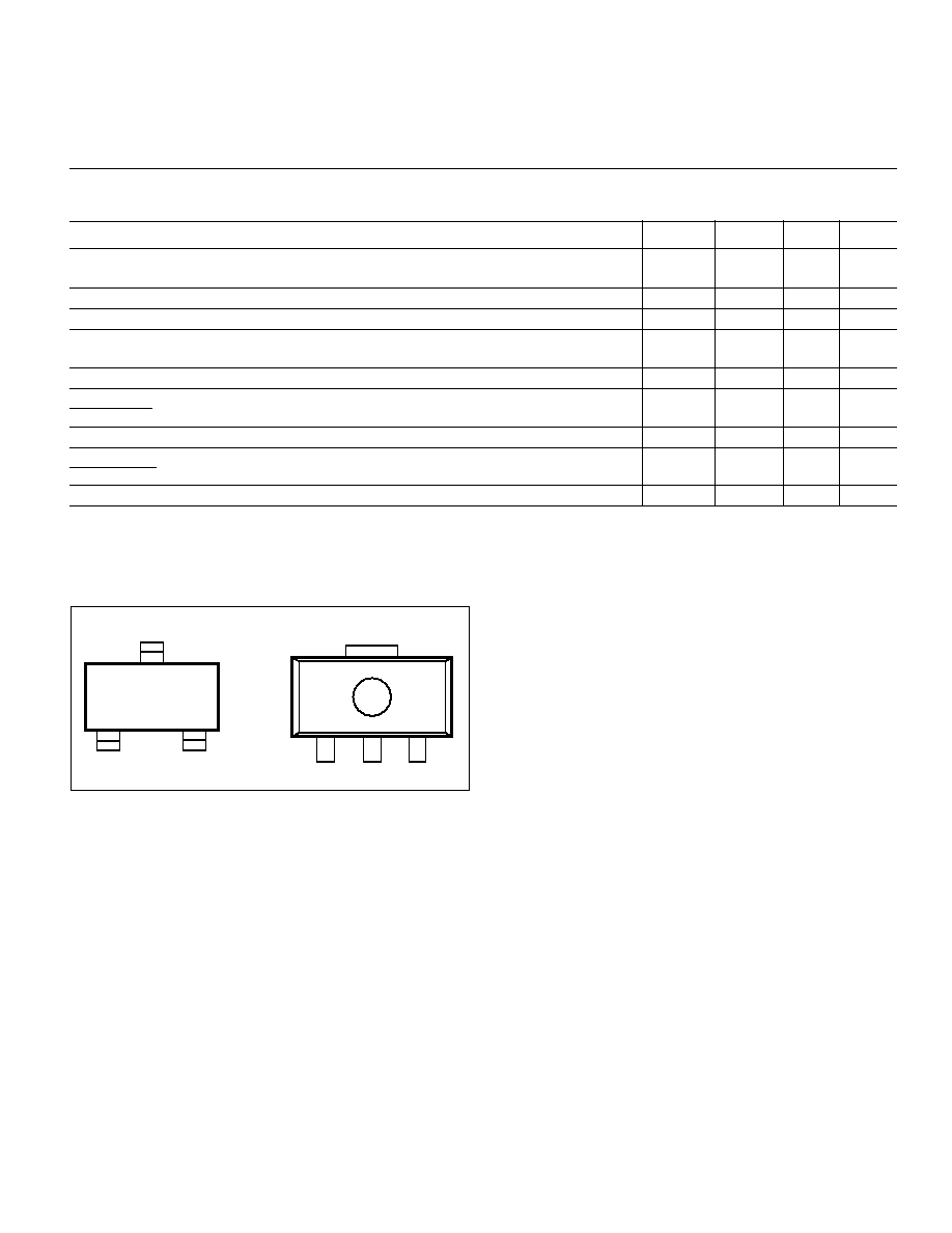
MARKING
3-Pin SOT-23A
3-Pin SOT-89
x
x
*Static-sensitive device. Unused devices must be stored in conductive material. Protect devices from static discharge and static fields. Stresses above those
listed under Absolute Maximum Ratings may cause permanent damage to the device. These are stress ratings only and functional operation of the device
at these or any other conditions above those indicated in the operational sections of the specifications is not implied. Exposure to Absolute Maximum Rating
Conditions for extended periods may affect device reliability.
represents first voltage digit
2
3
4
5
6
ex: 3.xv =
kkkk
represents first decimal place voltage (x.0 - x.9)
A = x.0
E = x.4
L = x.8
B = x.1
F = x.5
M = x.9
C = x.2
H = x.6
D = x.3
K = x.7
ex: 3.4V =
kkkk
represents Polarity
0 = Positive (fixed)
represents assembly lot number
3
3
E
TC55 Series
5
1
µ
A LOW DROPOUT POSITIVE VOLTAGE REGULATOR
© 2001 Microchip Technology Inc. DS21435A
TC55-24 02/01/01
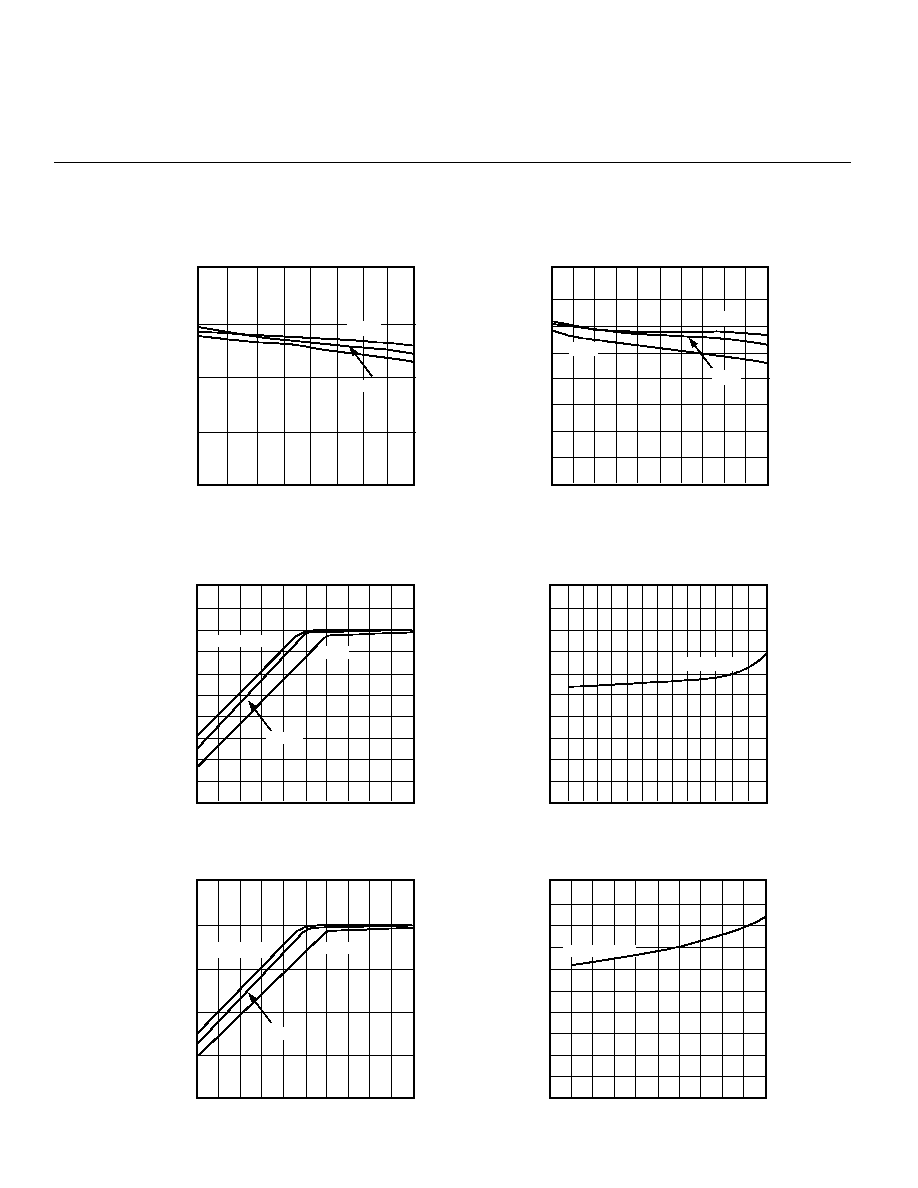
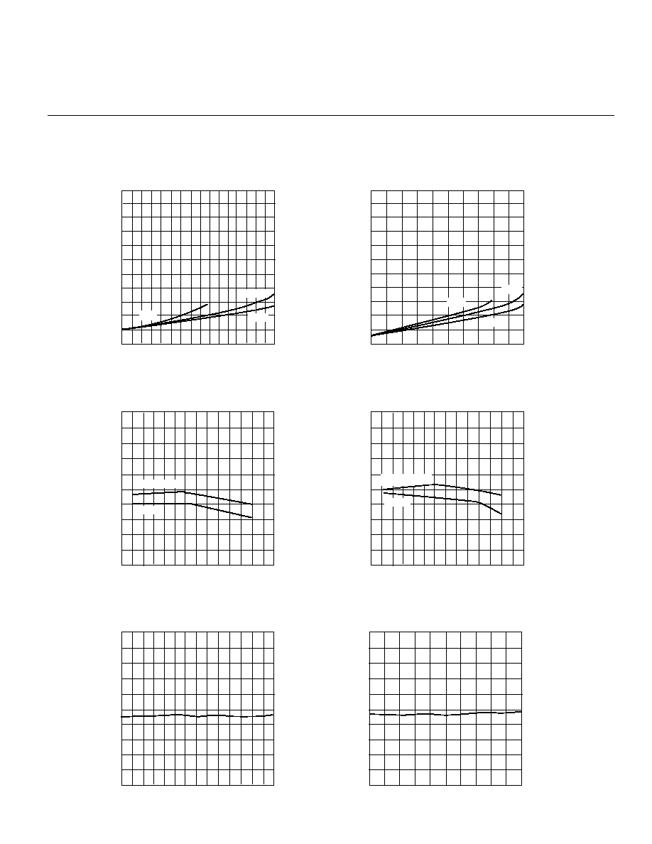
TYPICAL CHARACTERISTICS
0.8
0.6
0.4
0.2
0.0
0.2
20 40
60
0
160
OUTPUT CURRENT IOUT (mA)
OUTPUT CURRENT IOUT (mA)
TC55RP3002
1.4
1.2
1.0
2.0
1.8
1.6
DROPOUT VOLTAGE V
DIF
(V)
DROPOUT VOLTAGE V
DIF
(V)
3. DROPOUT VOLTAGE vs. OUTPUT CURRENT
4. OUTPUT VOLTAGE vs. OPERATING TEMPERATURE
80 100 120 140
25
°
C
1.0
0.8
0.6
0.4
0.2
0.0
0.2
40
80
0
200
160
TC55RP5002
1.4
1.2
2.0
1.8
1.6
120
OPERATING TEMPERATURE (
°
C)
3.02
3.00
2.98
2.96
2.94
2.92
2.90
40
20
0
20
40
60
80
100
TC55RP3002 (
VIN
= 4.0V)
3.06
3.04
3.10
3.08
OUTPUT VOLTAGE V
OUT
(V)
IOUT = 10mA
40mA
30
°
C
30
°
C
25
°
C
OPERATING TEMPERATURE (
°
C)
5.02
5.00
4.98
4.96
4.94
4.92
4.90
40
20
0
20
40
60
80
100
TC55RP5002 (
VIN
= 6.0V)
5.06
5.04
5.10
5.08
OUTPUT VOLTAGE V
OUT
(V)
IOUT = 10mA
40mA
5. SUPPLY CURRENT vs. INPUT VOLTAGE
INPUT VOLTAGE VIN (V)
1.1
1.0
0.9
0.8
0.7
0.6
0.5
3
4
5
6
7
8
9
10
INPUT VOLTAGE VIN (V)
5
6
7
8
9
10
TC55RP3002
1.3
1.2
1.5
1.4
SUPPLY CURRENT I
SS
(
µ
A)
1.6
1.4
1.3
1.2
1.1
1.0
0.5
1.8
1.7
2.0
1.9
SUPPLY CURRENT I
SS
(
µ
A)
T
OPR
= 25
°
C
T
OPR
= 25
°
C
TC55RP5002
80
°
C
80
°
C