1µA Low Dropout Positive Voltage Regulator
2003 Microchip Technology Inc.
DS21435E-page 1
M
TC55
Features
· Low Dropout Voltage: 120 mV (typ) at 100 mA,
380 mV (typ) at 200 mA
· High Output Current: 250 mA (V
OUT
= 5.0V)
· High Accuracy Output Voltage: ±2% (max)
(±1% Semi-Custom Version)
· Low Power Consumption: 1.1 µA (typ)
· Low Temperature Drift: ±100 ppm/°C (typ)
· Excellent Line Regulation: 0.2%/V (typ)
· Package Options: 3-Pin SOT-23A, 3-Pin SOT-89
and 3-Pin TO-92
· Short-Circuit Protection
· Standard Output Voltage Options: 1.2V, 1.8V,
2.5V, 3.0V, 3.3V, 5.0V
Applications
· Battery-Powered Devices
· Cameras and Portable Video Equipment
· Pagers and Cellular Phones
· Solar Powered Instruments
· Consumer Products
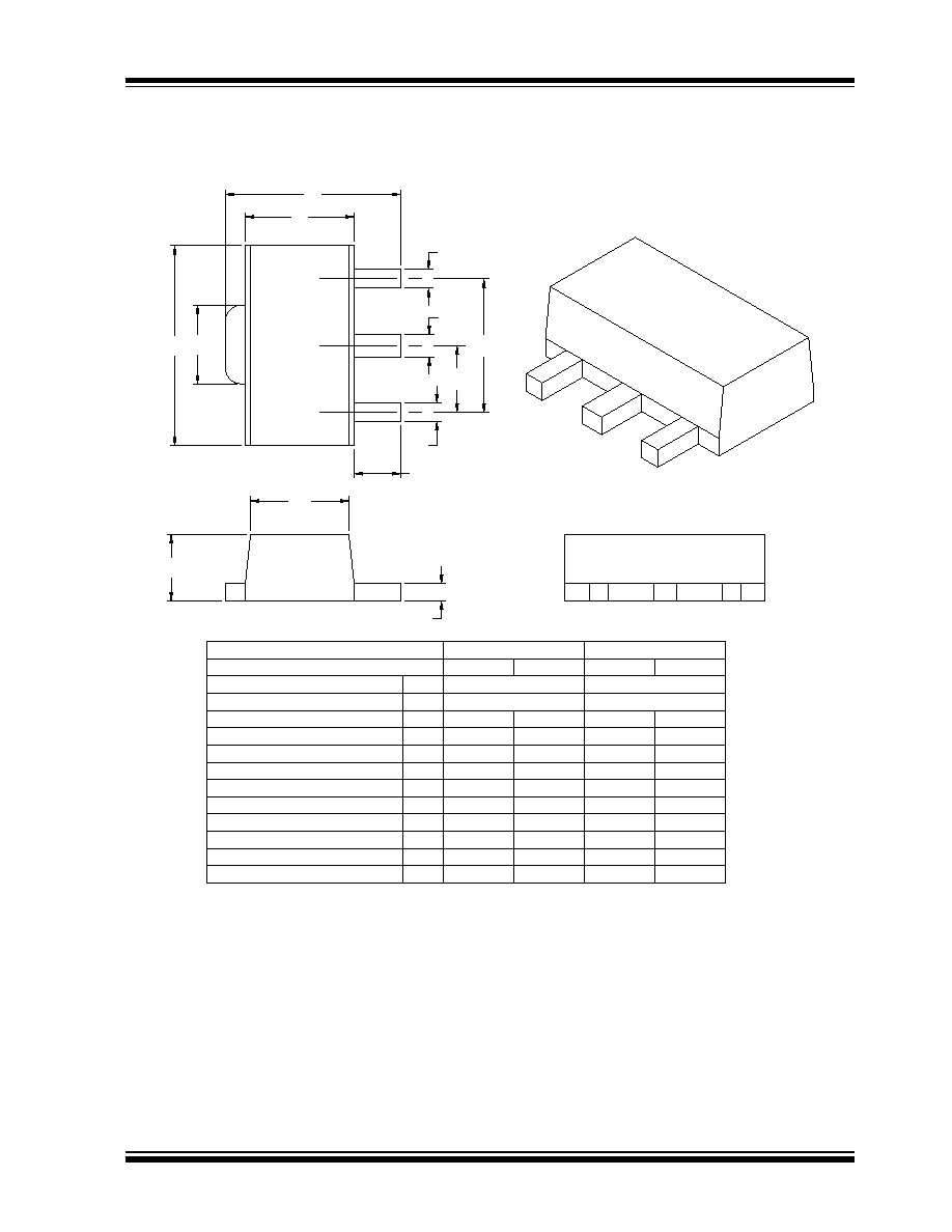
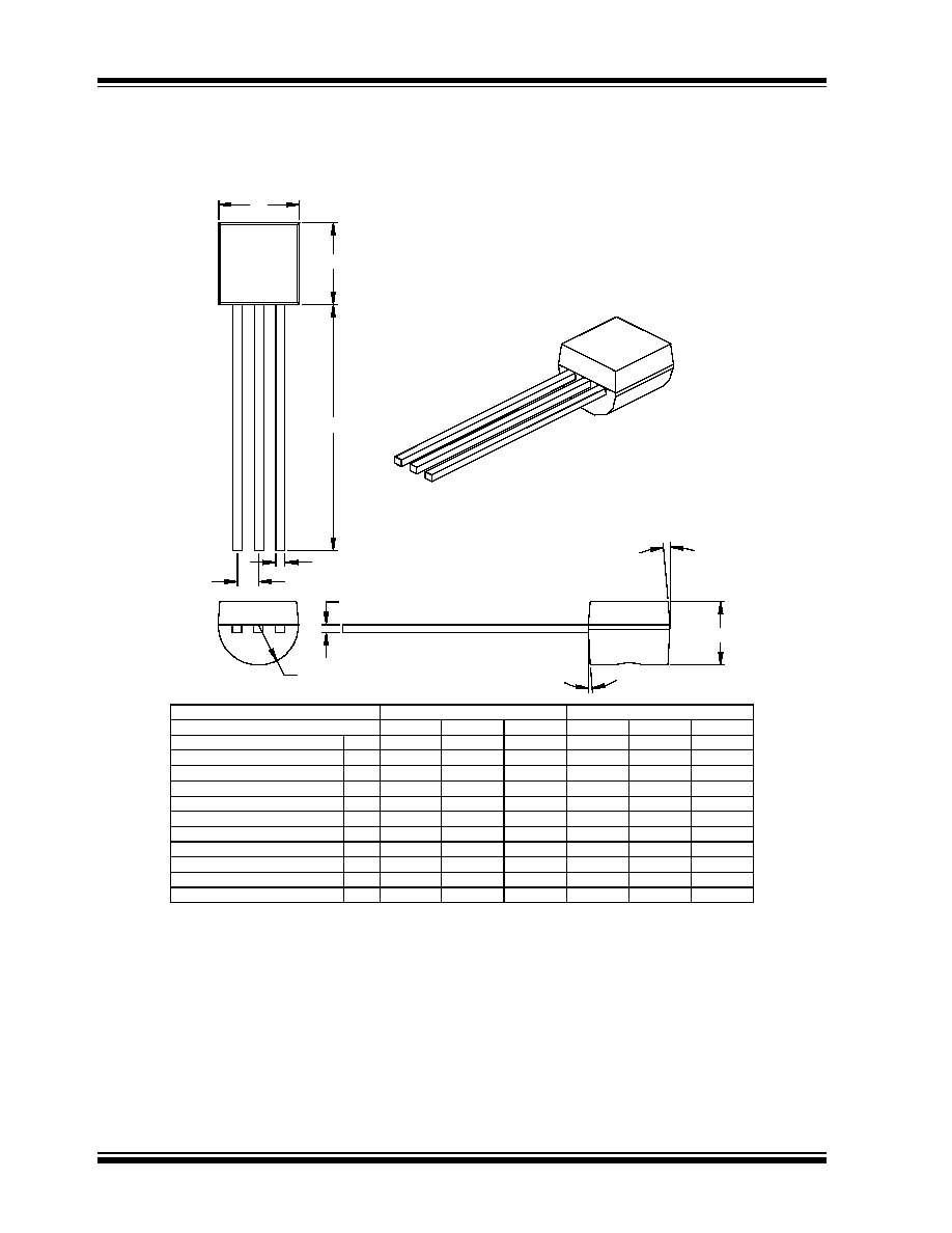
Package Types
General Description
The TC55 Series is a collection of CMOS low dropout,
positive voltage regulators that can source up to
250 mA of current, with an extremely low input-output
voltage differential of 380 mV (typ) at 200 mA.
The TC55's low dropout voltage, combined with the low
current consumption of only 1.1 µA (typ), makes it ideal
for battery operation. The low voltage differential (drop-
out voltage) extends the battery operating lifetime. It
also permits high currents in small packages when
operated with minimum V
IN
V
OUT
differentials.
The circuit also incorporates short-circuit protection to
ensure maximum reliability.
Functional Block Diagram
V
IN
GND
V
OUT
3
1
2
TC55
GND V
IN
V
OUT
1
2
3
TC55
3-Pin SOT-23A
3-Pin SOT-89
3-Pin TO-92
1 2 3
V
OUT
V
IN
GND
Note: 3-Pin SOT-23A is equivalent to the
EIAJ SC-59.
V
IN
Bottom
View
V
IN
V
OUT
GND
Short-Circuit
Protection
Voltage
Reference
+
1 µA Low Dropout Positive Voltage Regulator
TC55
DS21435E-page 2
2003 Microchip Technology Inc.
1.0
ELECTRICAL
CHARACTERISTICS
Absolute Maximum Ratings
Input Voltage ........................................................+12V
Output Current (Continuous) ......... P
D
/(V
IN
V
OUT
)mA
Output Current (peak) ..................................... 500 mA
Output Voltage ................. (V
SS
0.3V) to (V
IN
+ 0.3V)
Continuous Power Dissipation:
3-Pin SOT-23A ..........................................240 mW
3-Pin SOT-89 ............................................500 mW
3-Pin TO-92...............................................440 mW
Stresses above those listed under "Absolute Maximum
Ratings" may cause permanent damage to the device. These
are stress ratings only and functional operation of the device
at these or any other conditions above those indicated in the
operation sections of the specifications is not implied.
Exposure to Absolute Maximum Rating conditions for
extended periods may affect device reliability.
PIN FUNCTION TABLE
TC55RP50: ELECTRICAL CHARACTERISTICS
TC55RP40: ELECTRICAL CHARACTERISTICS
Symbol
Description
GND
Ground Terminal
V
OUT
Regulated Voltage Output
V
IN
Unregulated Supply Input
Electrical Specifications: Unless otherwise specified, V
OUT
(S) = 5.0V, T
A
= +25°C (see Note 1).
Parameters
Sym
Min
Typ
Max
Units
Conditions
Output Voltage
V
OUT
(A)
--
4.90
--
5.0
--
5.10
V
I
OUT
= 40 mA
V
IN
= 6.0V
Maximum Output Current
I
OUT
MAX
250
--
--
mA
V
IN
= 6.0V, V
OUT
(A)
4.5V
Load Regulation
V
OUT
--
40
80
mV
V
IN
= 6.0V, 1 mA
I
OUT
100 mA
I/O Voltage Difference
V
DIF
--
--
120
380
300
600
mV
I
OUT
= 100 mA
I
OUT
= 200 mA
Current Consumption
I
SS
--
1.1
3.0
µA
V
IN
= 6.0V
Voltage Regulation
V
OUT
(A)·100
V
IN
·V
OUT
(S)
--
0.2
0.3
%/V
I
OUT
= 40 mA, 6.0V
V
IN
10.0V
Input Voltage
V
IN
--
--
10
V
Temperature Coefficient of Output
Voltage
V
OUT
(A)·10
6
V
OUT
(S)·
T
A
--
±100
--
ppm/°C I
OUT
= 40 mA, -40°C
T
A
+85°C
Long-Term Stability
--
0.5
--
%
T
A
= +125°C, 1000 Hours
Note 1:
V
OUT
(S): Preset value of output voltage; V
OUT
(A): Actual value of output voltage; V
DIF
: Definition of I/O voltage
difference = {V
IN
1 V
OUT
(A)}; V
OUT
(A): Output voltage when I
OUT
is fixed and V
IN
= V
OUT
(S) + 1.0V; V
IN
1: Input voltage
when the output voltage is 98% V
OUT
(A).
Electrical Specifications: Unless otherwise specified, V
OUT
(S) = 4.0V, T
A
= +25°C (see Note 1).
Parameters
Sym
Min
Typ
Max
Units
Conditions
Output Voltage
V
OUT
(A)
--
3.92
--
4.0
--
4.08
V
I
OUT
= 40 mA
V
IN
= 5.0V
Maximum Output Current
I
OUT
MAX
200
--
--
mA
V
IN
= 5.0V, V
OUT
(A)
3.6V
Load Regulation
V
OUT
--
45
90
mV
V
IN
= 5.0V, 1 mA
I
OUT
100 mA
I/O Voltage Difference
V
DIF
--
--
170
400
330
630
mV
I
OUT
= 100 mA
I
OUT
= 200 mA
Current Consumption
I
SS
--
1.0
2.9
µA
V
IN
= 5.0V
Voltage Regulation
V
OUT
(A)·100
V
IN
·V
OUT
(S)
--
0.2
0.3
%/V
I
OUT
= 40 mA, 5.0V
V
IN
10.0V
Input Voltage
V
IN
--
--
10
V
Temperature Coefficient of Output
Voltage
V
OUT
(A)·10
6
V
OUT
(S)·
T
A
--
±100
--
ppm/°C I
OUT
= 40 mA, -40°C
T
A
+85°C
Long-Term Stability
--
0.5
--
%
T
A
= +125°C, 1000 Hours
Note 1:
V
OUT
(S): Preset value of output voltage; V
OUT
(A): Actual value of output voltage; V
DIF
: Definition of I/O voltage
difference = {V
IN
1 V
OUT
(A)}; V
OUT
(A): Output voltage when I
OUT
is fixed and V
IN
= V
OUT
(S) + 1.0V; V
IN
1: Input voltage
when the output voltage is 98% V
OUT
(A).
2003 Microchip Technology Inc.
DS21435E-page 3
TC55
TC55RP33: ELECTRICAL CHARACTERISTICS
TC55RP30: ELECTRICAL CHARACTERISTICS
Electrical Specifications: Unless otherwise specified, V
OUT
(S) = 3.3V, T
A
= +25°C (see Note 1).
Parameters
Sym
Min
Typ
Max
Units
Conditions
Output Voltage
V
OUT
(A)
--
3.23
--
3.30
--
3.37
V
I
OUT
= 40 mA
V
IN
= 4.3V
Maximum Output Current
I
OUT
MAX
150
--
--
mA
V
IN
= 4.3V, V
OUT
(A)
3.0V
Load Regulation
V
OUT
--
45
90
mV
V
IN
= 4.3V,
1 mA
I
OUT
80 mA
I/O Voltage Difference
V
DIF
--
--
180
400
360
700
mV
I
OUT
= 80 mA
I
OUT
= 160 mA
Current Consumption
I
SS
--
1.0
2.9
µA
V
IN
= 4.3V
Voltage Regulation
V
OUT
(A)·100
V
IN
·V
OUT
(S)
--
0.2
0.3
%/V
I
OUT
= 40 mA,
4.3V
I
OUT
10.0V
Input Voltage
V
IN
--
--
10
V
Temperature Coefficient of Output
Voltage
V
OUT
(A)·10
6
V
OUT
(S)·
T
A
--
±100
--
ppm/°C I
OUT
= 40 mA, -40°C
T
A
+85°C
Long-Term Stability
--
0.5
--
%
T
A
= +125°C, 1,000 Hours
Note 1:
V
OUT
(S): Preset value of output voltage; V
OUT
(A): Actual value of output voltage; V
DIF
: Definition of I/O voltage
difference = {V
IN
1 V
OUT
(A)}; V
OUT
(A): Output voltage when I
OUT
is fixed and V
IN
= V
OUT
(S) + 1.0V; V
IN
1: Input voltage
when the output voltage is 98% V
OUT
(A).
Electrical Specifications: Unless otherwise specified, V
OUT
(S) = 3.0V, T
A
= +25°C (see Note 1).
Parameters
Sym
Min
Typ
Max
Units
Conditions
Output Voltage
V
OUT
(A)
--
2.94
--
3.0
--
3.06
V
I
OUT
= 40 mA
V
IN
= 4.0V
Maximum Output Current
I
OUT
MAX
150
--
--
mA
V
IN
= 4.0V, V
OUT
(A)
2.7V
Load Regulation
V
OUT
--
45
90
mV
V
IN
= 4.0V, 1 mA
I
OUT
80 mA
I/O Voltage Difference
V
DIF
--
--
180
400
360
700
mV
I
OUT
= 80 mA
I
OUT
= 160 mA
Current Consumption
I
SS
--
0.9
2.8
µA
V
IN
= 4.0V
Voltage Regulation
V
OUT
(A)·100
V
IN
·V
OUT
(S)
--
0.2
0.3
%/V
I
OUT
= 40 mA, 4.0V
V
IN
10.0V
Input Voltage
V
IN
--
--
10
V
Temperature Coefficient of Output
Voltage
V
OUT
(A)·10
6
V
OUT
(S)·
T
A
--
±100
--
ppm/°C I
OUT
= 40 mA, -40°C
T
A
+85°C
Long-Term Stability
--
0.5
--
%
T
A
= +125°C, 1000 Hours
Note 1:
V
OUT
(S): Preset value of output voltage; V
OUT
(A): Actual value of output voltage; V
DIF
: Definition of I/O voltage
difference = {V
IN
1 V
OUT
(A)}; V
OUT
(A): Output voltage when I
OUT
is fixed and V
IN
= V
OUT
(S) + 1.0V; V
IN
1: Input voltage
when the output voltage is 98% V
OUT
(A).
TC55
DS21435E-page 4
2003 Microchip Technology Inc.
TC55RP25: ELECTRICAL CHARACTERISTICS
TC55RP18: ELECTRICAL CHARACTERISTICS
Electrical Specifications: Unless otherwise specified, V
OUT
(S) = 2.5V, T
A
= +25°C (see Note 1).
Parameters
Sym
Min
Typ
Max
Units
Conditions
Output Voltage
V
OUT
(A)
--
2.45
--
2.5
--
2.55
V
I
OUT
= 40 mA
V
IN
= 3.5V
Maximum Output Current
I
OUT
MAX
125
--
--
mA
V
IN
= 3.5V, V
OUT
(A)
2.25V
Load Regulation
V
OUT
--
45
90
mV
V
IN
= 3.5V,
1 mA
I
OUT
60 mA
I/O Voltage Difference
V
DIF
--
180
400
360
700
mV
I
OUT
= 60 mA
I
OUT
= 120 mA
Current Consumption
I
SS
--
1.0
2.8
µA
V
IN
= 3.5V
Voltage Regulation
V
OUT
(A)·100
V
IN
·V
OUT
(S)
--
0.2
0.3
%/V
I
OUT
= 40 mA,
3.5V
I
OUT
10.0V
Input Voltage
V
IN
--
--
10
V
Temperature Coefficient of Output
Voltage
V
OUT
(A)·10
6
V
OUT
(S)·
T
A
--
±100
--
ppm/°C I
OUT
= 40 mA, -30°C
T
A
+80°C
Long-Term Stability
--
0.5
--
%
T
A
= +125°C, 1,000 Hours
Note 1:
V
OUT
(S): Preset value of output voltage; V
OUT
(A): Actual value of output voltage; V
DIF
: Definition of I/O voltage
difference = {V
IN
1 V
OUT
(A)}; V
OUT
(A): Output voltage when I
OUT
is fixed and V
IN
= V
OUT
(S) + 1.0V; V
IN
1: Input voltage
when the output voltage is 98% V
OUT
(A).
Electrical Specifications: Unless otherwise specified, V
OUT
(S) = 1.8V, T
A
= +25°C (see Note 1).
Parameters
Sym
Min
Typ
Max
Units
Conditions
Output Voltage
V
OUT
(A)
--
1.764
--
1.8
--
1.836
V
I
OUT
= 0.5 mA
V
IN
= 2.8V
Maximum Output Current
I
OUT
MAX
110
--
--
mA
V
IN
= 2.8V, V
OUT
(A)
1.62V
Load Regulation
V
OUT
--
--
30
mV
V
IN
= 2.8V,
1 mA
I
OUT
30 mA
I/O Voltage Difference
V
DIF
--
--
300
mV
I
OUT
= 0.5 mA
Current Consumption
I
SS
--
--
3.0
µA
V
IN
= 2.8V
Voltage Regulation
V
OUT
(A)·100
V
IN
·V
OUT
(S)
--
--
0.25
%/V
I
OUT
= 0.5 mA,
2.8V
I
OUT
10.0V
Input Voltage
V
IN
--
--
6.0
V
Temperature Coefficient of Output
Voltage
V
OUT
(A)·10
6
V
OUT
(S)·
T
A
--
±100
--
ppm/°C I
OUT
= 0.5 mA, -30°C
T
A
+80°C
Long-Term Stability
--
0.5
--
%
T
A
= +125°C, 1,000 Hours
Note 1:
V
OUT
(S): Preset value of output voltage; V
OUT
(A): Actual value of output voltage; V
DIF
: Definition of I/O voltage
difference = {V
IN
1 V
OUT
(A)}; V
OUT
(A): Output voltage when I
OUT
is fixed and V
IN
= V
OUT
(S) + 1.0V; V
IN
1: Input voltage
when the output voltage is 98% V
OUT
(A).
2003 Microchip Technology Inc.
DS21435E-page 5
TC55
TC55RP12: ELECTRICAL CHARACTERISTICS
TEMPERATURE CHARACTERISTICS
Electrical Specifications: Unless otherwise specified, V
OUT
(S) = 1.2V, T
A
= +25°C (see Note 1).
Parameters
Sym
Min
Typ
Max
Units
Conditions
Output Voltage
V
OUT
(A)
--
1.176
--
1.200
--
1.224
V
I
OUT
= 0.5 mA
V
IN
= 2.2V
Maximum Output Current
I
OUT
MAX
50
--
--
mA
V
IN
= 2.2V, V
OUT
(A)
1.08V
Load Regulation
V
OUT
--
--
30
mV
V
IN
= 2.2V,
1 mA
I
OUT
30 mA
I/O Voltage Difference
V
DIF
--
--
300
mV
I
OUT
= 0.5 mA
Current Consumption
I
SS
--
--
3.0
µA
V
IN
= 2.2V
Voltage Regulation
V
OUT
(A)·100
V
IN
·V
OUT
(S)
--
--
0.25
%/V
I
OUT
= 0.5 ,
2.2V
I
OUT
10.0V
Input Voltage
V
IN
--
--
6.0
V
Temperature Coefficient of Output
Voltage
V
OUT
(A)·10
6
V
OUT
(S)·
T
A
--
±100
--
ppm/°C I
OUT
= 0.5 mA, -30°C
T
A
+80°C
Long-Term Stability
--
0.5
--
%
T
A
= +125°C, 1,000 Hours
Note 1:
V
OUT
(S): Preset value of output voltage; V
OUT
(A): Actual value of output voltage; V
DIF
: Definition of I/O voltage
difference = {V
IN
1 V
OUT
(A)}; V
OUT
(A): Output voltage when I
OUT
is fixed and V
IN
= V
OUT
(S) + 1.0V; V
IN
1: Input voltage
when the output voltage is 98% V
OUT
(A).
Electrical Specifications: Unless otherwise specified, V
OUT
(S) = 5.0V, T
A
= +25°C.
Parameters
Sym
Min
Typ
Max
Units
Conditions
Temperature Ranges
Specified Temperature Range (E)
T
A
-40
--
+85
ºC
Storage Temperature Range
T
A
-65
--
+150
ºC
Package Thermal Resistances
Thermal Resistance, 3L-SOT-23A
JA
--
359
--
ºC/W
Thermal Resistance, 3L-SOT-89
JA
--
110
--
ºC/W
When mounted on 1 square
inch of copper
Thermal Resistance, 3L-TO-92
JA
--
131.9
--
ºC/W
TC55
DS21435E-page 6
2003 Microchip Technology Inc.
2.0
TYPICAL PERFORMANCE CURVES
Notes: Unless otherwise specified, V
OUT
(S) = 3.0V, 5.0V, T
A
= +25°C, C
IN
= 1 µF Tantalum, C
OUT
= 1 µF Tantalum.
FIGURE 2-1:
Output Voltage vs. Output
Current (TC55RP3002).
FIGURE 2-2:
Output Voltage vs. Input
Voltage (TC55RP3002).
FIGURE 2-3:
Output Voltage vs. Input
Voltage (TC55RP3002).
FIGURE 2-4:
Dropout Voltage vs. Output
Current (TC55RP3002).
FIGURE 2-5:
Output Voltage vs.
Operating Temperature (TC55RP3002).
FIGURE 2-6:
Supply Current vs. Input
Voltage (TC55RP3002).
Note:
The graphs and tables provided following this note are a statistical summary based on a limited number of
samples and are provided for informational purposes only. The performance characteristics listed herein
are not tested or guaranteed. In some graphs or tables, the data presented may be outside the specified
operating range (e.g., outside specified power supply range) and therefore outside the warranted range.
2.9
2.8
2.7
20
40
60
0
160
OUTPUT CURRENT I
OUT
(mA)
3.0
3.1
OUTPUT VOLTAGE V
OUT
(V)
80
°C
80 100 120 140
25
°C
-30
°C
V
IN
= 4.0V
T
OPR
= 25
°C
INPUT VOLTAGE V
IN
(V)
2.8
2.6
2.4
2.2
3.0
3.5
2.5
3.0
3.2
OUTPUT VOLTAGE V
OUT
(V)
I
OUT
= 1 mA
10 mA
40 mA
T
OPR
= 25
°C
INPUT VOLTAGE V
IN
(V)
OUTPUT VOLTAGE V
OUT
(V)
3.01
3.00
2.99
2.98
2.96
2.97
2.95
5
6
7
8
9
10
3
4
3.03
3.02
3.05
3.04
I
OUT
= 1 mA
0.8
0.6
0.4
0.2
0.0
-0.2
20 40
60
0
160
OUTPUT CURRENT I
OUT
(mA)
1.4
1.2
1.0
2.0
1.8
1.6
DROPOUT VOLTAGE V
DIF
(V)
80 100 120 140
25
°C
-30
°C
80
°C
OPERATING TEMPERATURE (
°C)
3.02
3.00
2.98
2.96
2.94
2.92
2.90
-40
-20
0
20
40
60
80
100
3.06
3.04
3.10
3.08
OUTPUT VOLTAGE V
OUT
(V)
I
OUT
= 10 mA
40 mA
V
IN
= 4.0V
INPUT VOLTAGE V
IN
(V)
1.1
1.0
0.9
0.8
0.7
0.6
0.5
3
4
5
6
7
8
9
10
1.3
1.2
1.5
1.4
SUPPLY CURRENT I
SS
(
µ
A)
T
OPR
= 25
°
C
2003 Microchip Technology Inc.
DS21435E-page 7
TC55
Note: Unless otherwise indicated, V
OUT
(S) = 3.0V, 5.0V, T
A
= +25°C, C
IN
= 1 µF Tantalum, C
OUT
= 1 µF Tantalum.
FIGURE 2-7:
Supply Current vs.
Operating Temperature (TC55RP3002).
FIGURE 2-8:
Load Transient Response
(TC55RP3002).
FIGURE 2-9:
Output Voltage vs. Output
Current (TC55RP5002).
FIGURE 2-10:
Output Voltage vs. Input
Voltage (TC55RP5002).
FIGURE 2-11:
Output Voltage vs. Input
Voltage (TC55RP5002).
FIGURE 2-12:
Dropout Voltage vs. Output
Current (TC55RP5002).
0.9
0.8
0.7
0.6
0.5
-20
0
20
-40
OPERATING TEMPERATURE (
°C)
1.2
1.1
1.0
1.5
1.4
1.8
40
60
80 100
SUPPLY CURRENT I
SS
(
µ
A)
V
IN
= 4.0V
TIME (2 msec/div)
4
3
2
1
0
40 mA
1 mA
5
200
160
120
80
40
0
OUTPUT VOLTAGE V
OUT
(V)
OUTPUT CURRENT I
OUT
(mA)
Output Current
Output Voltage
OUTPUT CURRENT I
OUT
(mA)
4.9
4.8
4.7
40
80
0
200
160
5.0
5.1
OUTPUT VOLTAGE V
OUT
(V)
120
80
°C
25
°C
-30
°C
V
IN
= 6.0V
INPUT VOLTAGE V
IN
(V)
T
OPR
= 25
°C
4.8
4.6
4.4
4.2
5.0
5.5
4.5
5.0
5.2
OUTPUT VOLTAGE V
OUT
(V)
I
OUT
= 1 mA
10 mA
40 mA
INPUT VOLTAGE V
IN
(V)
T
OPR
= 25
°C
5.01
5.00
4.99
4.97
4.98
4.95
4.98
6
7
8
9
10
5
5.03
5.02
5.04
5.05
OUTPUT VOLTAGE V
OUT
(V)
IOUT = 1 mA
OUTPUT CURRENT I
OUT
(mA)
DROPOUT VOLTAGE V
DIF
(V)
1.0
0.8
0.6
0.4
0.2
0.0
-0.2
40
80
0
200
160
1.4
1.2
2.0
1.8
1.6
120
-30
°C
25
°C
80
°C
TC55
DS21435E-page 8
2003 Microchip Technology Inc.
Note: Unless otherwise indicated, V
OUT
(S) = 3.0V, 5.0V, T
A
= +25°C, C
IN
= 1 µF Tantalum, C
OUT
= 1 µF Tantalum.
FIGURE 2-13:
Output Voltage vs.
Operating Temperature (TC55RP5002).
FIGURE 2-14:
Supply Current vs. Input
Voltage (TC55RP5002).
FIGURE 2-15:
Supply Current vs.
Operating Temperature (TC55RP5002).
FIGURE 2-16:
Input Transient Response,
1 mA (TC55RP5002).
FIGURE 2-17:
Input Transient Response,
10 mA (TC55RP5002).
FIGURE 2-18:
Load Transient Response
(TC55RP5002).
OPERATING TEMPERATURE (
°C)
5.02
5.00
4.98
4.96
4.94
4.92
4.90
-40
-20
0
20
40
60
80
100
5.06
5.04
5.10
5.08
OUTPUT VOLTAGE V
OUT
(V)
I
OUT
= 10 mA
40 mA
V
IN
= 6.0V
INPUT VOLTAGE V
IN
(V)
5
6
7
8
9
10
1.6
1.4
1.3
1.2
1.1
1.0
0.5
1.8
1.7
2.0
1.9
SUPPLY CURRENT I
SS
(
µ
A)
T
OPR
= 25
°
C
1.4
1.3
1.2
1.1
1.0
-20
0
20
-40
OPERATING TEMPERATURE (
°C)
1.7
1.6
1.5
2.0
1.9
1.8
40
60
80 100
SUPPLY CURRENT I
SS
(
µ
A)
V
IN
= 6.0V
TIME (msec)
7.0
6.5
6.0
5.5
5.0
5.0
4.5
4.0
-1
0
1
2
3
7.5
Input
Voltage
Output
Voltage
8.0
INPUT VOLTAGE V
OUT
(V)
OUTPUT VOLTAGE V
IN
(V)
I
OUT
= 1 mA
TIME (msec)
7.0
6.5
6.0
5.5
5.0
4.5
4.0
-1
0
1
2
3
7.5
Input
Voltage
Output
Voltage
8.0
INPUT VOLTAGE V
OUT
(V)
OUTPUT VOLTAGE V
OUT
(V)
I
OUT
= 10 mA
TIME (2 msec/div)
6
5
4
3
2
40 mA
1 mA
7
200
160
120
80
40
0
OUTPUT VOLTAGE V
OUT
(V)
OUTPUT CURRENT I
OUT
(mA)
Output Voltage
Output Current
2003 Microchip Technology Inc.
DS21435E-page 9
TC55
3.0
PIN DESCRIPTIONS
The descriptions of the pins are listed in Table 3-1.
TABLE 3-1:
PIN FUNCTION TABLE
3.1
Ground Terminal (GND)
Regulator ground. Tie GND to the negative side of the
output and the negative side of the input capacitor.
Only the LDO bias current (1 µA typical) flows out of
this pin, there is no high current. The LDO output regu-
lation is referenced to this pin. Minimize voltage drops
between this pin and the minus side of the load.
3.2
Regulated Voltage Output (V
OUT
)
Connect V
OUT
to the positive side of the load and the
positive terminal of the output capacitor. The positive
side of the output capacitor should be physically
located as close to the LDO V
OUT
pin as is practical.
The current flowing out of this pin is equal to the DC
load current.
3.3
Unregulated Supply Input (V
IN
)
Connect the input supply voltage and the positive side
of the input capacitor to V
IN
. The input capacitor should
be physically located as close as is practical to V
IN
. The
current flow into this pin is equal to the DC load current,
plus the LDO bias current (1 µA typical.)
4.0
DETAILED DESCRIPTION
The TC55 is a low quiescent current, precision, fixed-
output voltage LDO. Unlike bipolar regulators, the
TC55 supply current does not increase proportionally
with load current.
4.1
Output Capacitor
A minimum of 1 µF output capacitor is required. The
output capacitor should have an effective series resis-
tance (esr) greater than 0.1
and less than 5, plus a
resonant frequency above 1 MHz. Larger output
capacitors can be used to improve supply noise rejec-
tion and transient response. Care should be taken
when increasing C
OUT
to ensure that the input imped-
ance is not high enough to cause high input impedance
oscillation.
4.2
Input Capacitor
A 1 µF input capacitor is recommended for most
applications when the input impedance is on the order
of 10
. Larger input capacitance may be required for
stability when operating off of a battery input, or if there
is a large distance from the input source to the LDO.
When large values of output capacitance are used, the
input capacitance should be increased to prevent high
source impedance oscillations.
Pin No.
Symbol
Description
1
GND
Ground Terminal
2
V
OUT
Regulated Voltage Output
3
V
IN
Unregulated Supply Input
TC55
DS21435E-page 10
2003 Microchip Technology Inc.
5.0
THERMAL CONSIDERATIONS
5.1
Power Dissipation
The amount of power dissipated internal to the low
dropout linear regulator is the sum of the power dissi-
pation within the linear pass device (P-Channel MOS-
FET) and the quiescent current required to bias the
internal reference and error amplifier. The internal lin-
ear pass device power dissipation is calculated by mul-
tiplying the voltage across the linear device by the
current through the device.
EQUATION
The internal power dissipation, as a result of the bias
current for the LDO internal reference and error
amplifier, is calculated by multiplying the ground or
quiescent current by the input voltage.
EQUATION
The total internal power dissipation is the sum of P
D
(Pass Device) and P
D
(Bias).
EQUATION
For the TC55, the internal quiescent bias current is so
low (1 µA typical) that the P
D
(Bias) term of the power
dissipation equation can be ignored. The maximum
power dissipation can be estimated by using the
maximum input voltage and the minimum output
voltage to obtain a maximum voltage differential
between input and output. The next step would be to
multiply the maximum voltage differential by the
maximum output current.
EQUATION
Given:
V
IN
= 3.3V to 4.1V
V
OUT
= 3.0 V ± 2%
I
OUT
= 1 mA to 100 mA
T
AMAX
= 55°C
P
MAX
= (4.1V (3.0V x 0.98)) x 100 mA
P
MAX
= 116.0 milliwatts
To determine the junction temperature of the device, the
thermal resistance from junction-to-ambient must be
known. The 3-pin SOT-23 thermal resistance from junc-
tion-to-air (R
JA
) is estimated to be approximately
359°C/W. The SOT-89 R
JA
is estimated to be approxi-
mately 110°C/W when mounted on 1 square inch of
copper. The TO-92 R
JA
is estimated to be 131.9°C/W.
The R
JA
will vary with physical layout, airflow and other
application-specific conditions.
The device junction temperature is determined by
calculating the junction temperature rise above
ambient, then adding the rise to the ambient
temperature.
EQUATION
P
D
(Pass Device) = (V
IN
V
OUT
) x I
OUT
P
D
(Bias) = V
IN
x I
GND
P
TOTAL
= P
D
(Pass Device) + P
D
(Bias)
P
D
= (V
INMAX
V
OUTMIN
) x I
OUTMAX
Junction Temperature
T
J
= P
DMAX
x R
JA
+ T
A
T
J
= 116.0 milliwatts x 359°C/W + 55°C
T
J
= 96.6°C
SOT-23 Example:
SOT-89 Example:
T
J
= 116.0 milliwatts x 110°C/W + 55°C
T
J
= 67.8°C
TO-92 Example:
T
J
= 116.0 milliwatts x 131.9°C/W + 55°C
T
J
= 70.3°C
2003 Microchip Technology Inc.
DS21435E-page 11
TC55
6.0
PACKAGING INFORMATION
6.1
Package Marking Information
Symbol
Voltage
Symbol
Voltage
A
x.0
F
x.5
B
x.1
H
x.6
C
x.2
K
x.7
D
x.3
L
x.8
E
x.4
M
x.9
3-Pin SOT-23A
3-Pin SOT-89
1
1
2
2
4
3
4
3
1
represents first voltage digit
2V, 3V, 4V, 5V, 6V
Ex: 3.xV =
3
2
represents first decimal place voltage (x.0 - x.9)
Ex: 3.4V =
3 E
3
represents polarity
0 = Positive (fixed)
4
represents assembly lot number
3-Pin TO-92
8
12
4
7
11
3
6
10
2
5
9
1
= 55RP (fixed)
1 , 2 , 3 & 4
5
represents first voltage digit (2-6)
6
represents first voltage decimal (0-9)
7
represents extra feature code: fixed: 0
represents regulation accuracy
8
1 = ±1.0% (custom), 2 = ±2.0% (standard)
9 , 10,
represents assembly lot number
11 & 12
TC55
DS21435E-page 12
2003 Microchip Technology Inc.
3-Lead Plastic Small Outline Transistor (CB) (SOT23)
10
5
0
10
5
0
Mold Draft Angle Bottom
10
5
0
10
5
0
Mold Draft Angle Top
0.51
0.44
0.37
.020
.017
.015
B
Lead Width
0.18
0.14
0.09
.007
.006
.004
c
Lead Thickness
10
5
0
10
5
0
Foot Angle
0.55
0.45
0.35
.022
.018
.014
L
Foot Length
3.04
2.92
2.80
.120
.115
.110
D
Overall Length
1.40
1.30
1.20
.055
.051
.047
E1
Molded Package Width
2.64
2.37
2.10
.104
.093
.083
E
Overall Width
0.10
0.06
0.01
.004
.002
.000
A1
Standoff §
1.02
0.95
0.88
.040
.037
.035
A2
Molded Package Thickness
1.12
1.01
0.89
.044
.040
.035
A
Overall Height
1.92
.076
p1
Outside lead pitch (basic)
0.96
.038
p
Pitch
3
3
n
Number of Pins
MAX
NOM
MIN
MAX
NOM
MIN
Dimension Limits
MILLIMETERS
INCHES*
Units
2
1
p
D
B
n
E
E1
L
c
A2
A
A1
p1
* Controlling Parameter
Notes:
Dimensions D and E1 do not include mold flash or protrusions. Mold flash or protrusions shall not exceed
.010" (0.254mm) per side.
JEDEC Equivalent: TO-236
Drawing No. C04-104
§ Significant Characteristic
2003 Microchip Technology Inc.
DS21435E-page 13
TC55
3-Lead Plastic Small Outline Transistor (MB) (SOT89)
0.56
0.44
.022
.017
B
Lead 2 Width
0.44
0.35
.017
.014
c
Lead Thickness
1.83
1.62
.072
.064
D1
Tab Length
4.60
4.40
.181
.173
D
Overall Length
2.29
2.13
.090
.084
E1
Molded Package Width at Top
4.25
3.94
.167
.155
H
Overall Width
1.60
1.40
.063
.055
A
Overall Height
3.00 BSC
.118 BSC
p1
Outside lead pitch (basic)
1.50 BSC
.059 BSC
p
Pitch
MAX
MIN
MAX
MIN
Dimension Limits
MILLIMETERS*
INCHES
Units
exceed .005" (0.127mm) per side.
Dimensions D and E1 do not include mold flash or protrusions. Mold flash or protrusions shall not
Notes:
JEDEC Equivalent: TO-243
Drawing No. C04-29
*Controlling Parameter
Foot Length
L
.035
.047
0.89
1.20
Leads 1 & 3 Width
B1
.014
.019
0.36
0.48
Molded Package Width at Base
E
.090
.102
2.29
2.60
D1
H
L
B1
B
B1
p
p1
E
C
A
D
1
2
3
E1
TC55
DS21435E-page 14
2003 Microchip Technology Inc.
3-Lead Plastic Transistor Outline (ZB) (TO-92)
4
3
2
4
3
2
Mold Draft Angle Bottom
6
5
4
6
5
4
0.56
0.48
0.41
.022
.019
.016
B
Lead Width
0.51
0.43
0.36
.020
.017
.014
c
Lead Thickness
2.41
2.29
2.16
.095
.090
.085
R
Molded Package Radius
4.95
4.64
4.32
.195
.183
.170
D
Overall Length
4.95
4.71
4.45
.195
.186
.175
E1
Overall Width
3.94
3.62
3.30
.155
.143
.130
A
Bottom to Package Flat
1.27
.050
p
Pitch
3
3
n
Number of Pins
MAX
NOM
MIN
MAX
NOM
MIN
Dimension Limits
MILLIMETERS
INCHES*
Units
R
n
1
3
p
L
B
A
c
1
D
2
E1
Tip to Seating Plane
L
.500
.555
.610
12.70
14.10
15.49
*Controlling Parameter
Mold Draft Angle Top
Notes:
Dimensions D and E1 do not include mold flash or protrusions. Mold flash or protrusions shall not exceed
.010" (0.254mm) per side.
JEDEC Equivalent: TO-92
Drawing No. C04-101
2003 Microchip Technology Inc.
DS21435E-page 15
TC55
PRODUCT IDENTIFICATION SYSTEM
To order or obtain information, e.g., on pricing or delivery, refer to the factory or the listed sales office
.
Sales and Support
Device:
TC55: 1 µA Low Dropout Positive Voltage Regulator
Output Voltage:
12
= 1.2V "Standard"
18
= 1.8V "Standard"
25
= 2.5V "Standard"
30
= 3.0V "Standard"
33
= 3.3V "Standard"
50
= 5.0V "Standard"
Extra Feature Code:
0
= Fixed
Tolerance:
1
= 1.0% (Custom)
2
= 2.0% (Standard)
Temperature:
E
= -40
°C to +85°C
Package Type:
CB = 3-Pin SOT-23A (equivalent to EIAJ SC-59)
MB = 3-Pin SOT-89
ZB = 3-Pin TO-92
Taping Direction:
TR = Standard
713 = Standard
PART NO.
X
XX
Output Feature
Code
Device
Examples:
a)
TC55RP1802ECB713: 1.8V LDO Positive
Voltage Regulator, 2% Tolerance
SOT23-A-3 package.
b)
TC55RP2502EMB713: 1.8V LDO Positive
Voltage Regulator, 2% Tolerance.
SOT89-3 package.
c)
TC55RP2502ECB713: 2.5V LDO Positive
Voltage Regulator, 2% Tolerance.
SOT23-A-3 package.
d)
TC55RP3002ECB713: 3.0V LDO Positive
Voltage Regulator, 2% Tolerance.
SOT23-A-3 package.
e)
TC55RP3002EMB713: 3.0V LDO Positive
Voltage Regulator, 2% Tolerance.
SOT89-3 package.
f)
TC55RP3302ECB713: 3.3V LDO Positive
Voltage Regulator, 2% Tolerance.
SOT23-A-3 package.
g)
TC55RP3302EMB713: 3.3V LDO Positive
Voltage Regulator, 2% Tolerance.
SOT89-3 package.
h)
TC55RP5002ECB713: 5.0V LDO Positive
Voltage Regulator, 2% Tolerance.
SOT23-A-3 package.
i)
TC55RP5002EMB713: 5.0V LDO Positive
Voltage Regulator, 2% Tolerance.
SOT89-3 package.
Voltage
X
Tolerance
X
Temp.
XX
Package
XX
Taping
Direction
Data Sheets
Products supported by a preliminary Data Sheet may have an errata sheet describing minor operational differences and
recommended workarounds. To determine if an errata sheet exists for a particular device, please contact one of the following:
1.
Your local Microchip sales office
2.
The Microchip Corporate Literature Center U.S. FAX: (480) 792-7277
3.
The Microchip Worldwide Site (www.microchip.com)
Please specify which device, revision of silicon and Data Sheet (include Literature #) you are using.
Customer Notification System
Register on our web site (www.microchip.com/cn) to receive the most current information on our products.

TC55
DS21435E-page 16
2003 Microchip Technology Inc.
NOTES:
2003 Microchip Technology Inc.
DS21435E-page 17
Information contained in this publication regarding device
applications and the like is intended through suggestion only
and may be superseded by updates. It is your responsibility to
ensure that your application meets with your specifications.
No representation or warranty is given and no liability is
assumed by Microchip Technology Incorporated with respect
to the accuracy or use of such information, or infringement of
patents or other intellectual property rights arising from such
use or otherwise. Use of Microchip's products as critical
components in life support systems is not authorized except
with express written approval by Microchip. No licenses are
conveyed, implicitly or otherwise, under any intellectual
property rights.
Trademarks
The Microchip name and logo, the Microchip logo, K
EE
L
OQ
,
MPLAB, PIC, PICmicro, PICSTART, PRO MATE and
PowerSmart are registered trademarks of Microchip
Technology Incorporated in the U.S.A. and other countries.
FilterLab, microID, MXDEV, MXLAB, PICMASTER, SEEVAL
and The Embedded Control Solutions Company are
registered trademarks of Microchip Technology Incorporated
in the U.S.A.
Accuron, Application Maestro, dsPIC, dsPICDEM,
dsPICDEM.net, ECONOMONITOR, FanSense, FlexROM,
fuzzyLAB, In-Circuit Serial Programming, ICSP, ICEPIC,
microPort, Migratable Memory, MPASM, MPLIB, MPLINK,
MPSIM, PICC, PICkit, PICDEM, PICDEM.net, PowerCal,
PowerInfo, PowerMate, PowerTool, rfLAB, rfPIC, Select
Mode, SmartSensor, SmartShunt, SmartTel and Total
Endurance are trademarks of Microchip Technology
Incorporated in the U.S.A. and other countries.
Serialized Quick Turn Programming (SQTP) is a service mark
of Microchip Technology Incorporated in the U.S.A.
All other trademarks mentioned herein are property of their
respective companies.
© 2003, Microchip Technology Incorporated, Printed in the
U.S.A., All Rights Reserved.
Printed on recycled paper.
Note the following details of the code protection feature on Microchip devices:
·
Microchip products meet the specification contained in their particular Microchip Data Sheet.
·
Microchip believes that its family of products is one of the most secure families of its kind on the market today, when used in the
intended manner and under normal conditions.
·
There are dishonest and possibly illegal methods used to breach the code protection feature. All of these methods, to our
knowledge, require using the Microchip products in a manner outside the operating specifications contained in Microchip's Data
Sheets. Most likely, the person doing so is engaged in theft of intellectual property.
·
Microchip is willing to work with the customer who is concerned about the integrity of their code.
·
Neither Microchip nor any other semiconductor manufacturer can guarantee the security of their code. Code protection does not
mean that we are guaranteeing the product as "unbreakable."
Code protection is constantly evolving. We at Microchip are committed to continuously improving the code protection features of our
products. Attempts to break microchip's code protection feature may be a violation of the Digital Millennium Copyright Act. If such acts
allow unauthorized access to your software or other copyrighted work, you may have a right to sue for relief under that Act.
Microchip received QS-9000 quality system
certification for its worldwide headquarters,
design and wafer fabrication facilities in
Chandler and Tempe, Arizona in July 1999
and Mountain View, California in March 2002.
The Company's quality system processes and
procedures are QS-9000 compliant for its
PICmicro
®
8-bit MCUs, K
EE
L
OQ
®
code hopping
devices, Serial EEPROMs, microperipherals,
non-volatile memory and analog products. In
addition, Microchip's quality system for the
design and manufacture of development
systems is ISO 9001 certified.

DS21435E-page 18
2003 Microchip Technology Inc.
M
AMERICAS
Corporate Office
2355 West Chandler Blvd.
Chandler, AZ 85224-6199
Tel: 480-792-7200 Fax: 480-792-7277
Technical Support: 480-792-7627
Web Address: http://www.microchip.com
Atlanta
3780 Mansell Road, Suite 130
Alpharetta, GA 30022
Tel: 770-640-0034 Fax: 770-640-0307
Boston
2 Lan Drive, Suite 120
Westford, MA 01886
Tel: 978-692-3848 Fax: 978-692-3821
Chicago
333 Pierce Road, Suite 180
Itasca, IL 60143
Tel: 630-285-0071 Fax: 630-285-0075
Dallas
4570 Westgrove Drive, Suite 160
Addison, TX 75001
Tel: 972-818-7423 Fax: 972-818-2924
Detroit
Tri-Atria Office Building
32255 Northwestern Highway, Suite 190
Farmington Hills, MI 48334
Tel: 248-538-2250 Fax: 248-538-2260
Kokomo
2767 S. Albright Road
Kokomo, IN 46902
Tel: 765-864-8360 Fax: 765-864-8387
Los Angeles
18201 Von Karman, Suite 1090
Irvine, CA 92612
Tel: 949-263-1888 Fax: 949-263-1338
Phoenix
2355 West Chandler Blvd.
Chandler, AZ 85224-6199
Tel: 480-792-7966 Fax: 480-792-4338
San Jose
Microchip Technology Inc.
2107 North First Street, Suite 590
San Jose, CA 95131
Tel: 408-436-7950 Fax: 408-436-7955
Toronto
6285 Northam Drive, Suite 108
Mississauga, Ontario L4V 1X5, Canada
Tel: 905-673-0699 Fax: 905-673-6509
ASIA/PACIFIC
Australia
Microchip Technology Australia Pty Ltd
Marketing Support Division
Suite 22, 41 Rawson Street
Epping 2121, NSW
Australia
Tel: 61-2-9868-6733 Fax: 61-2-9868-6755
China - Beijing
Microchip Technology Consulting (Shanghai)
Co., Ltd., Beijing Liaison Office
Unit 915
Bei Hai Wan Tai Bldg.
No. 6 Chaoyangmen Beidajie
Beijing, 100027, No. China
Tel: 86-10-85282100 Fax: 86-10-85282104
China - Chengdu
Microchip Technology Consulting (Shanghai)
Co., Ltd., Chengdu Liaison Office
Rm. 2401-2402, 24th Floor,
Ming Xing Financial Tower
No. 88 TIDU Street
Chengdu 610016, China
Tel: 86-28-86766200 Fax: 86-28-86766599
China - Fuzhou
Microchip Technology Consulting (Shanghai)
Co., Ltd., Fuzhou Liaison Office
Unit 28F, World Trade Plaza
No. 71 Wusi Road
Fuzhou 350001, China
Tel: 86-591-7503506 Fax: 86-591-7503521
China - Hong Kong SAR
Microchip Technology Hongkong Ltd.
Unit 901-6, Tower 2, Metroplaza
223 Hing Fong Road
Kwai Fong, N.T., Hong Kong
Tel: 852-2401-1200 Fax: 852-2401-3431
China - Shanghai
Microchip Technology Consulting (Shanghai)
Co., Ltd.
Room 701, Bldg. B
Far East International Plaza
No. 317 Xian Xia Road
Shanghai, 200051
Tel: 86-21-6275-5700 Fax: 86-21-6275-5060
China - Shenzhen
Microchip Technology Consulting (Shanghai)
Co., Ltd., Shenzhen Liaison Office
Rm. 1812, 18/F, Building A, United Plaza
No. 5022 Binhe Road, Futian District
Shenzhen 518033, China
Tel: 86-755-82901380 Fax: 86-755-8295-1393
China - Qingdao
Rm. B505A, Fullhope Plaza,
No. 12 Hong Kong Central Rd.
Qingdao 266071, China
Tel: 86-532-5027355 Fax: 86-532-5027205
India
Microchip Technology Inc.
India Liaison Office
Marketing Support Division
Divyasree Chambers
1 Floor, Wing A (A3/A4)
No. 11, O'Shaugnessey Road
Bangalore, 560 025, India
Tel: 91-80-2290061 Fax: 91-80-2290062
Japan
Microchip Technology Japan K.K.
Benex S-1 6F
3-18-20, Shinyokohama
Kohoku-Ku, Yokohama-shi
Kanagawa, 222-0033, Japan
Tel: 81-45-471- 6166 Fax: 81-45-471-6122
Korea
Microchip Technology Korea
168-1, Youngbo Bldg. 3 Floor
Samsung-Dong, Kangnam-Ku
Seoul, Korea 135-882
Tel: 82-2-554-7200 Fax: 82-2-558-5934
Singapore
Microchip Technology Singapore Pte Ltd.
200 Middle Road
#07-02 Prime Centre
Singapore, 188980
Tel: 65-6334-8870 Fax: 65-6334-8850
Taiwan
Microchip Technology (Barbados) Inc.,
Taiwan Branch
11F-3, No. 207
Tung Hua North Road
Taipei, 105, Taiwan
Tel: 886-2-2717-7175 Fax: 886-2-2545-0139
EUROPE
Austria
Microchip Technology Austria GmbH
Durisolstrasse 2
A-4600 Wels
Austria
Tel: 43-7242-2244-399
Fax: 43-7242-2244-393
Denmark
Microchip Technology Nordic ApS
Regus Business Centre
Lautrup hoj 1-3
Ballerup DK-2750 Denmark
Tel: 45-4420-9895 Fax: 45-4420-9910
France
Microchip Technology SARL
Parc d'Activite du Moulin de Massy
43 Rue du Saule Trapu
Batiment A - ler Etage
91300 Massy, France
Tel: 33-1-69-53-63-20 Fax: 33-1-69-30-90-79
Germany
Microchip Technology GmbH
Steinheilstrasse 10
D-85737 Ismaning, Germany
Tel: 49-89-627-144-0
Fax: 49-89-627-144-44
Italy
Microchip Technology SRL
Via Quasimodo, 12
20025 Legnano (MI)
Milan, Italy
Tel: 39-0331-742611 Fax: 39-0331-466781
United Kingdom
Microchip Ltd.
505 Eskdale Road
Winnersh Triangle
Wokingham
Berkshire, England RG41 5TU
Tel: 44-118-921-5869 Fax: 44-118-921-5820
05/30/03
W
ORLDWIDE
S
ALES
AND
S
ERVICE
Document Outline