2003 Microchip Technology Inc.
DS21756B-page 1
M
TC642B/TC647B
Features
· Temperature-Proportional Fan Speed for Acoustic
Noise Reduction and Longer Fan Life
· Efficient PWM Fan Drive
· 3.0V to 5.5V Supply Range:
- Fan Voltage Independent of TC642B/TC647B
Supply Voltage
- Supports any Fan Voltage
· FanSense
TM
Fault Detection Circuit Protects
Against Fan Failure and Aids System Testing
· Shutdown Mode for "Green" Systems
· Supports Low Cost NTC/PTC Thermistors
· Over-Temperature Indication (TC642B only)
· Fan Auto-Restart
· Space-Saving 8-Pin MSOP Package
Applications
· Personal Computers & Servers
· LCD Projectors
· Datacom & Telecom Equipment
· Fan Trays
· File Servers
· General Purpose Fan Speed Control
Package Types
Description
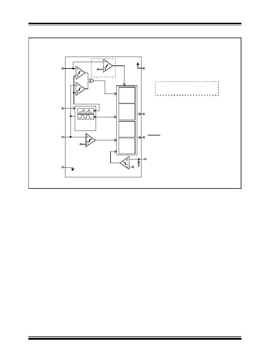
The TC642B/TC647B devices are new versions of the
existing TC642/TC647 fan speed controllers. These
devices are switch mode, fan speed controllers that
incorporate a new fan auto-restart function. Tempera-
ture-proportional speed control is accomplished using
pulse width modulation. A thermistor (or other voltage
output temperature sensor) connected to the V
IN
input
supplies the required control voltage of 1.20V to 2.60V
(typical) for 0% to 100% PWM duty cycle. Minimum fan
speed is set by a simple resistor divider on the V
MIN
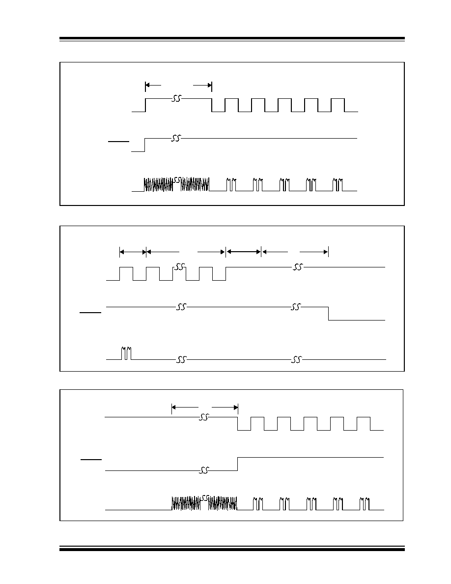
input. An integrated Start-Up Timer ensures reliable
motor start-up at turn-on, coming out of shutdown
mode or following a transient fault. A logic-low applied
to V
MIN
(pin 3) causes fan shutdown.
The TC642B and TC647B also feature Microchip
Technology's proprietary FanSense
TM
technology for
increasing system reliability. In normal fan operation, a
pulse train is present at SENSE (pin 5). A missing-
pulse detector monitors this pin during fan operation. A
stalled, open or unconnected fan causes the TC642B/
TC647B device to turn the V
OUT
output on full (100%
duty cycle). If the fault persists (a fan current pulse is
not detected within a 32/f period), the FAULT output
goes low. Even with the FAULT output low, the V
OUT
output is on full during the fan fault condition in order to
attempt to restart the fan. FAULT is also asserted if the
PWM reaches 100% duty cycle (TC642B only), indicat-
ing that maximum cooling capability has been reached
and a possible overheating condition exists.
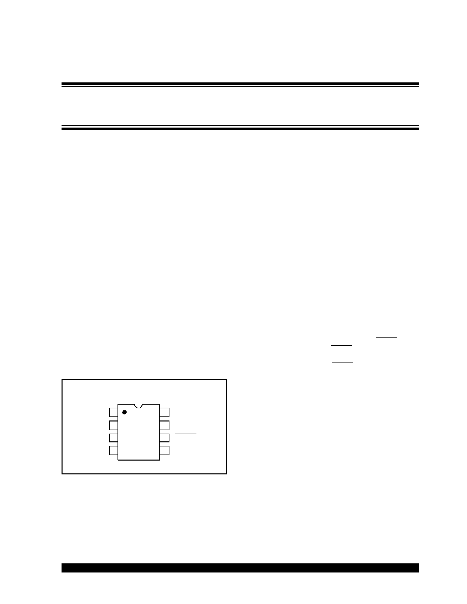
The TC642B and TC647B devices are available in 8-pin
plastic MSOP, SOIC and PDIP packages. The specified
temperature range of these devices is -40 to +85ºC.
MSOP, PDIP, SOIC
1
2
3
4
V
DD
5
6
7
8
V
OUT
SENSE
V
IN
C
F
V
MIN
GND
FAULT
TC642B
TC647B
PWM Fan Speed Controllers With Minimum Fan Speed,
Fan Restart and FanSenseTM Technology for Fault Detection
2003 Microchip Technology Inc.
DS21756B-page 3
TC642B/TC647B
1.0
ELECTRICAL
CHARACTERISTICS
Absolute Maximum Ratings
Supply Voltage (V
DD
) .......................................................6.0V
Input Voltage, Any Pin................(GND - 0.3V) to (V
DD
+0.3V)
Operating Temperature Range ....................- 40°C to +125°C
Maximum Junction Temperature, T
J
........................... +150°C
ESD Protection on all pins ........................................... > 3 kV
Notice: Stresses above those listed under "Maximum
Ratings" may cause permanent damage to the device. This is
a stress rating only and functional operation of the device at
those or any other conditions above those indicated in the
operational listings of this specification is not implied. Expo-
sure to maximum rating conditions for extended periods may
affect device reliability.
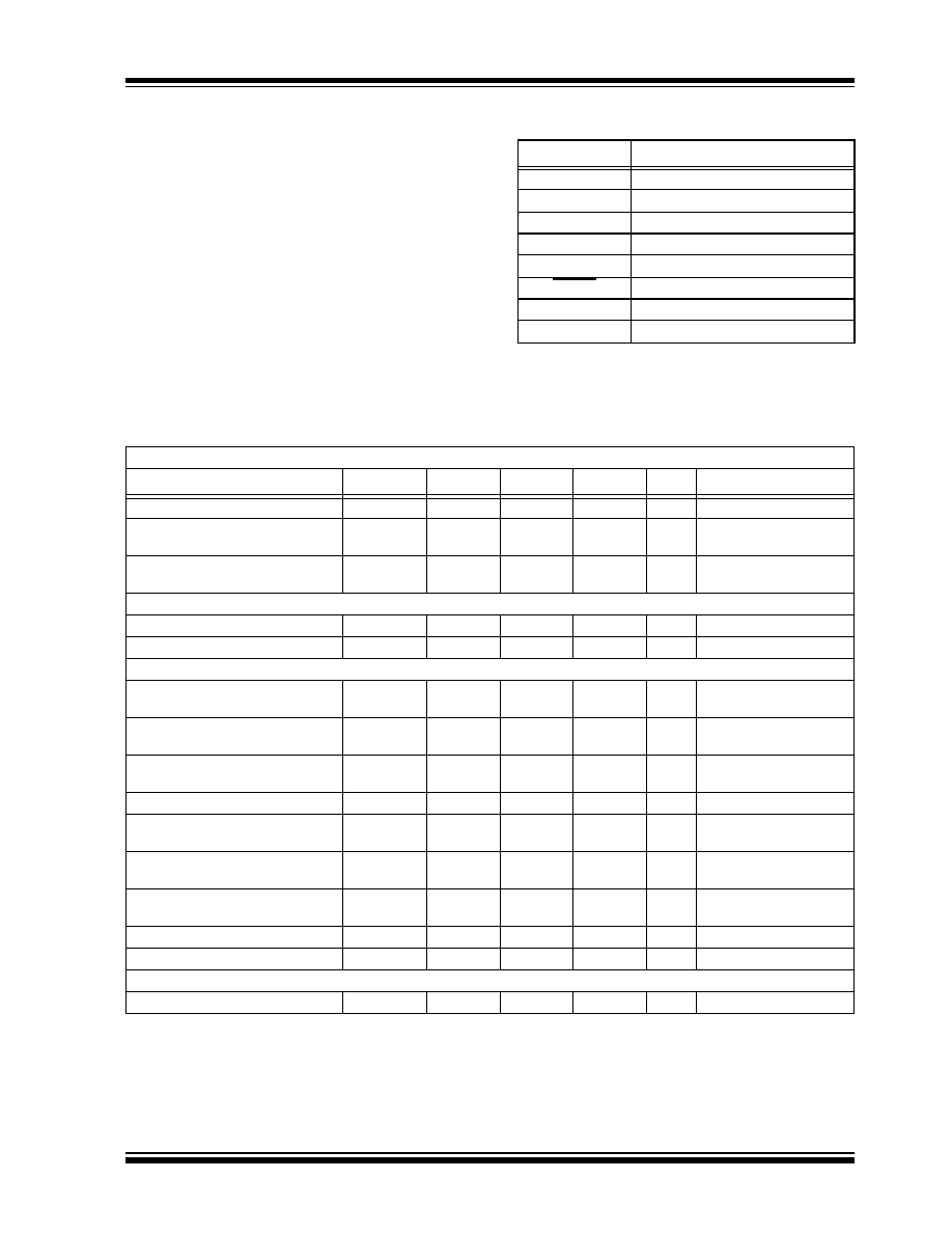
PIN FUNCTION TABLE
Name
Function
V
IN
Analog Input
C
F
Analog Output
V
MIN
Analog Input
GND
Ground
SENSE
Analog Input
FAULT
Digital (Open-Drain) Output
V
OUT
Digital Output
V
DD
Power Supply Input
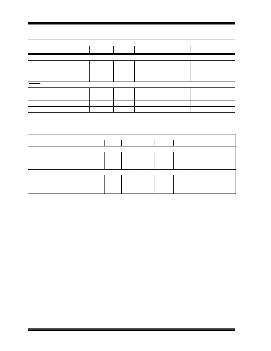
ELECTRICAL SPECIFICATIONS
Electrical Specifications: Unless otherwise specified, all limits are specified for -40°C < T
A
< +85°C, V
DD
= 3.0V to 5.5V.
Parameters
Sym
Min
Typ
Max
Units
Conditions
Supply Voltage
V
DD
3.0
--
5.5
V
Supply Current, Operating
I
DD
--
200
400
µA
Pins 6, 7 Open,
C
F
= 1 µF, V
IN
= V
C(MAX)
Supply Current, Shutdown Mode
I
DD(SHDN)
--
30
--
µA
Pins 6, 7 Open,
C
F
= 1 µF, V
MIN
= 0.35V
V
OUT
Output
Sink Current at V
OUT
Output
I
OL
1.0
--
--
mA
V
OL
= 10% of V
DD
Source Current at V
OUT
Output
I
OH
5.0
--
--
mA
V
OH
= 80% of V
DD
V
IN
, V
MIN
Inputs
Input Voltage at V
IN
or V
MIN
for 100%
PWM Duty Cycle
V
C(MAX)
2.45
2.60
2.75
V
Over-Temperature Indication
Threshold
V
OTF
V
C(MAX)
+
20 mV
V
For TC642B Only
Over-Temperature Indication
Threshold Hysteresis
V
OTF-HYS
80
mV
For TC642B Only
V
C(MAX)
- V
C(MIN)
V
C(SPAN)
1.3
1.4
1.5
V
Minimum Speed Threshold
V
MIN
V
C(MAX)
-
V
C(SPAN)
V
C(MAX)
V
Voltage Applied to V
MIN
to Ensure
Shutdown Mode
V
SHDN
--
--
V
DD
x 0.13
V
Voltage Applied to V
MIN
to Release
Shutdown Mode
V
REL
V
DD
x 0.19
--
--
V
V
DD
= 5V
Hysteresis on V
SHDN
, V
REL
V
HYST
--
0.03 x V
DD
--
V
V
IN
, V
MIN
Input Leakage
I
IN
- 1.0
--
+1.0
µA
Note 1
Pulse-Width Modulator
PWM Frequency
f
PWM
26
30
34
Hz
C
F
= 1.0 µF
Note 1:
Ensured by design, tested during characterization.
2:
For V
DD
< 3.7V, t
STARTUP
and t
MP
timers are typically 13/f.
TC642B/TC647B
DS21756B-page 4
2003 Microchip Technology Inc.
TEMPERATURE SPECIFICATIONS
SENSE Input
SENSE Input Threshold Voltage with
Respect to GND
V
TH(SENSE)
50
70
90
mV
Blanking time to ignore pulse due to
V
OUT
turn-on
t
BLANK
--
3.0
--
µsec
FAULT Output
Output Low Voltage
V
OL
--
--
0.3
V
I
OL
= 2.5 mA
Missing Pulse Detector Timer
t
MP
--
32/f
--
sec
Note 2
Start-Up Timer
t
STARTUP
--
32/f
--
sec
Note 2
Diagnostic Timer
t
DIAG
--
3/f
--
sec
Electrical Characteristics: Unless otherwise noted, all parameters apply at V
DD
= 3.0V to 5.5V
Parameters
Symbol
Min
Typ
Max
Units
Conditions
Temperature Ranges:
Specified Temperature Range
T
A
-40
--
+85
°C
Operating Temperature Range
T
A
-40
--
+125
°C
Storage Temperature Range
T
A
-65
--
+150
°C
Thermal Package Resistances:
Thermal Package Resistance, 8-Pin MSOP
JA
--
200
--
°C/W
Thermal Package Resistance, 8-Pin SOIC
JA
--
155
--
°C/W
Thermal Package Resistance, 8-Pin PDIP
JA
--
125
--
°C/W
ELECTRICAL SPECIFICATIONS (CONTINUED)
Electrical Specifications: Unless otherwise specified, all limits are specified for -40°C < T
A
< +85°C, V
DD
= 3.0V to 5.5V.
Parameters
Sym
Min
Typ
Max
Units
Conditions
Note 1:
Ensured by design, tested during characterization.
2:
For V
DD
< 3.7V, t
STARTUP
and t
MP
timers are typically 13/f.