
2004 Microchip Technology Inc.
DS21451D-page 1
M
TC6501/2/3/4
Features
∑ 5-Pin SOT-23A
∑ Factory-programmed Thresholds from
-45∞C to +125∞C in 10∞C Increments
∑ Pin Selectable +2∞C or +10∞C Hysteresis
∑ ±0.5∞C (Typ) Threshold Accuracy Over Full
Temperature Range
∑ No External Components Required
∑ 17 µA Supply Current (Typ)
Applications
∑ Thermal Management in PCs and Servers
∑ Over-temperature Fail-safe Circuits
∑ Simple Fan Controller
∑ Temperature Alarms
∑ Projectors/Printers
∑ Notebook Computers
∑ Network Boxes
Package Types
General Description
The TC6501/2/3/4 are SOT-23 temperature switches
that require no external components and are available
with factory-programmed temperature thresholds. A
choice of factory-trimmed temperature trip points are
also available. Pin-selectable hysteresis of +2∞C or
+10∞C allows flexibility to the design of the application.
These parts typically consume only 17 µA of current
and operate over the entire -55∞C to +135∞C
temperature range, while offering accuracies of ±0.5∞C
(typ).
The TC6501 and TC6503 have an open-drain, active-
low output, which targets microcontroller reset control.
The TC6502 and TC6504 have a CMOS, active-high
output designed to drive the logic level MOSFET that
turns on a fan or heater element.
The TC6501/TC6502 are designed for hot temperature
monitoring (+35∞C to +125∞C). These devices assert a
logic signal when the temperature goes above the
threshold. The TC6503/TC6504 are optimized for cold
temperature monitoring (-45∞C to +15∞C) and assert a
logic signal when the temperature goes below the
threshold.
The TC6501/2/3/4 are offered with five standard tem-
perature thresholds. Available in 5-Pin SOT-23A pack-
ages, these parts are ideal for applications requiring
high integration, small size, low power and low installed
cost.
Functional Block Diagram
T
OVER
TC6502
HYST
TC6501
TC6502
1
2
3
5
V
CC
GND
GND
4
Note: 5-Pin SOT-23A is equivalent to EIAJ SC-74A
T
UNDER
TC6503
T
UNDER
TC6504
HYST
TC6503
TC6504
1
2
3
5
V
CC
GND
GND
4
T
OVER
TC6501
GND GNDHYST
+2.7V to +5.5V
V
CC
INT
PICmicro
Æ
T
OVER
V
CC
TC6502
GND
100 pF
Microcontroller
Ultra Small Temperature Switches
with Pin Selectable Hysteresis

TC6501/2/3/4
DS21451D-page 2
2004 Microchip Technology Inc.
1.0
ELECTRICAL
CHARACTERISTICS
Absolute Maximum Ratings*
Supply Voltage (V
CC
) .............................. -0.3V to +7V
Input Current (All Pins).......................................20 mA
Output Current (All Pins) ....................................20 mA
Operating Temperature Range..........- 55∞C to +135∞C
Storage Temperature Range .............- 65∞C to +165∞C
T
OVER
(TC6501)....................................... -0.3V to +7V
T
OVER
(TC6502)......................... -0.3V to (V
CC
+ 0.3V)
T
UNDER
(TC6503)....................................... -0.3V to 7V
T
UNDER
(TC6504)....................... -0.3V to (V
CC
+ 0.3V)
All Other Pins ............................. -0.3V to (V
CC
+ 0.3V)
Maximum Junction Temperature, T
J
.................. 150∞C
Power Dissipation (T
A
= +70∞C):
(Derate 7.1 mW/∞C Above +70∞C) ...............570 mW
* Notice: Stresses above those listed under "Maximum
Ratings" may cause permanent damage to the device.
This is a stress rating only and functional operation of
the device at these or any other conditions above those
indicated in the operational sections of the specifica-
tions is not implied. Exposure to maximum rating con-
ditions for extended periods may affect device
reliability.
ELECTRICAL SPECIFICATIONS
Electrical Characteristics: Unless otherwise noted, V
CC
= +2.7V to +5.5V, R
PULL-UP
= 100 k
(TC6501/TC6503 only), 100 pF
decoupling capacitor from V
CC
to GND, T
AMB
= -55∞C to +135∞C. Typical values are at T
A
= +25∞C.
Parameter
Symbol
Min
Typ
Max
Unit
Test Conditions
Supply Voltage Range
V
CC
2.7
--
5.5
V
Supply Current
I
CC
--
17
40
µA
HYST Input Threshold
V
IH
0.8 x V
CC
--
--
V
HYST Input Threshold
V
IL
--
--
0.2 x V
CC
V
Temperature Threshold Accuracy (Note 1)
T
TH
-6
±0.5
6
∞C
-45∞C to -25∞C
-4
±0.5
4
∞C
-15∞C to +15∞C
-4
±0.5
4
∞C
+35∞C to +65∞C
-6
±0.5
6
∞C
+75∞C to +125∞C
Temperature Threshold Hysteresis
T
HYST
--
2.0
--
∞C
HYST = GND
--
10
--
∞C
HYST = V
CC
Output Voltage High
V
OH
0.8 x V
CC
--
--
V
I
SOURCE
= 500 µA, V
CC
> 2.7V
(TC6502/TC6504 Only)
V
CC
- 1.5
--
--
V
I
SOURCE
= 800 µA, V
CC
> 4.5V
(TC6502/TC6504 Only)
Output Voltage Low
V
OL
--
--
0.3
V
I
SINK
= 1.2 mA, V
CC
> 2.7V
--
--
0.4
V
I
SINK
= 3.2 mA, V
CC
> 4.5V
Open-Drain Output Leakage Current
--
10
--
nA
V
CC
= 2.7V, T
UNDER
= 5.5V
(TC6503); T
OVER
= 5.5V
(TC6501)
Note 1: The TC6501/2/3/4 are available with internal, factory-programmed temperature trip thresholds from -45∞C to +125∞C, in
+10∞C increments.
2004 Microchip Technology Inc.
DS21451D-page 3
TC6501/2/3/4
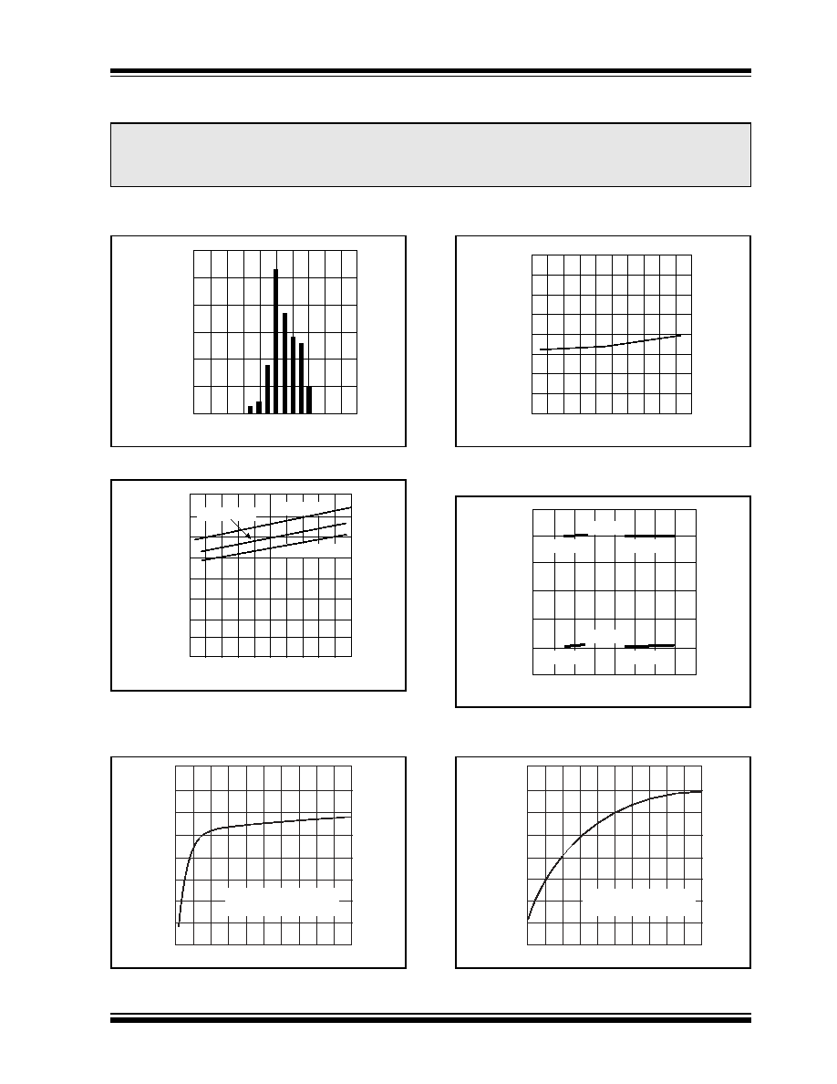
2.0
TYPICAL PERFORMANCE CURVES
Note:
Unless otherwise noted, V
CC
= 5.0V, R
PULL-UP
= 100 k
(TC6501/TC6503 only), 100 pF decoupling
capacitor from V
CC
to GND, T
AMB
= +25∞C.
.
FIGURE 2-1:
Trip Threshold Accuracy.
FIGURE 2-2:
Output Sink Resistance vs.
Temperature.
FIGURE 2-3:
Thermal Step Response in
Perfluorinated Fluid (SOT-23).
FIGURE 2-4:
Supply Current vs.
Temperature.
FIGURE 2-5:
Hysteresis vs. Trip
Temperature.
FIGURE 2-6:
Thermal Step Response in
Still Air (SOT-23).
Note:
The graphs and tables provided following this note are a statistical summary based on a limited number of
samples and are provided for informational purposes only. The performance characteristics listed herein
are not tested or guaranteed. In some graphs or tables, the data presented may be outside the specified
operating range (e.g., outside specified power supply range) and therefore outside the warranted range.
-5
-3
-4
-1
-2
1
0
3
2
5
4
Accuracy (∞C)
60
50
40
30
20
10
0
Frequency
0 10 20 30 40 50
Temperature (∞C)
Output Resistance (
)
80
70
60
50
40
30
20
10
0
60 70 80 90 100
V
CC
= 2.7V
V
CC
= 4.0V
V
CC
= 5.0V
+15∞C/div
+100∞C
+25∞C
5sec/div
Mounted On 0.75 in2
of 2 oz. Copper
-60 -40 -20 0 20 40
Temperature (∞C)
Supply Current (µA)
40
35
30
25
20
15
10
5
0
60 80 100 120 140
Trip Temperature (∞C)
Hysteresis (∞C)
-45
12
10
8
6
4
2
0
-25
-5
15 35 55 75 95 115
HYS = GND
HYST = V
CC
TC6503/04
TC6503/04
TC6501/02
TC6501/02
+12.5 C/div
+100∞C
+25∞C
20sec/div
Mounted On 0.75 in2
of 2 oz. Copper

TC6501/2/3/4
DS21451D-page 4
2004 Microchip Technology Inc.
Note:
Unless otherwise noted, V
CC
= 5.0V, R
PULL-UP
= 100 k
(TC6501/TC6503 only), 100 pF decoupling
capacitor from V
CC
to GND, T
AMB
= +25∞C.
FIGURE 2-7:
Output Source Resistance
vs. Temperature (TC6502).
0
20 40
60
80 100
Temperature (∞C)
Output Source Resistance (
)
180
160
140
120
100
80
60
180
40
20
140
120
VCC = 2.7V
VCC = 4.0V
VCC = 5.0V

2004 Microchip Technology Inc.
DS21451D-page 5
TC6501/2/3/4
3.0
PIN DESCRIPTIONS
The descriptions of the pins are listed in Table 3-1.
TABLE 3-1:
PIN FUNCTION TABLE
3.1
Ground
Connect the device ground pins directly to the PCB
ground and minimize the length of the connection. The
thermal resistance to the die is at a minimum at Pin 2.
3.2
Hysteresis Input (HYST)
Either 2∞C (GND) or 10∞C (V
CC
)
of hysteresis is
selected by connecting HYST to GND or V
CC
.
3.3
Supply Input (V
CC
)
A 100 pF or greater decoupling capacitor from V
CC
to
GND is recommended.
3.4
Open-Drain, Active-Low Output
(TC6501) (T
OVER
)
The voltage at the T
OVER
pin is equal to a logic-low
level if the sensor detects a temperature that is greater
than the factory-programmed threshold temperature.
Because this is an open-drain output, an external pull-
up resistor is required (a 100 k
pull-up resistor is
recommended). The voltage on this pin can be higher
than V
CC
, though the voltage must not exceed the
absolute maximum input voltage of 7.0V.
3.5
Push/Pull Active-High Output
(TC6502) (T
OVER
)
The voltage at T
OVER
is equal to a logic-high level if the
sensor detects a temperature greater than the factory-
programmed threshold temperature.
3.6
Open-Drain, Active-Low Output
(TC6503) (T
UNDER
)
The voltage at the T
UNDER
pin is equal to a logic-low
level if the sensor detects a temperature that is less
than the factory-programmed threshold temperature.
Because this is an open-drain output, an external pull-
up resistor is required (a 100 k
pull-up resistor is
recommended). The voltage on this pin can be higher
than V
CC
, though the voltage must not exceed the
absolute maximum input voltage of 7.0V
3.7
Push/Pull Active-High Output
(TC6504) (T
UNDER
)
The voltage at T
UNDER
is equal to a logic-high level if
the sensor detects a temperature less than the factory-
programmed threshold temperature.
TC6501
TC6502
TC6503
TC6504
Symbol
Description
1, 2
1, 2
1, 2
1, 2
GND
Ground
3
3
3
3
HYST
Hysteresis Input
4
4
4
4
V
CC
Supply Input (+2.7V to +5.5V)
5
--
--
--
T
OVER
Open-Drain, Active-Low Output
--
5
--
--
T
OVER
Push/Pull Active-High Output
--
--
5
--
T
UNDER
Open-Drain, Active-Low Output
--
--
--
5
T
UNDER
Push/Pull Active-High Output