
©
2002 Microchip Technology Inc.
DS21461B-page 1
TC7136/TC7136A
Features
∑ Fast Over Range Recovery, Ensured First Reading
Accuracy
∑ Low Temperature Drift Internal Reference
- TC7136: 70ppm/∞C (Typ.)
- TC7136A: 35ppm/∞C (Typ.)
∑ Zero Reading with Zero Input
∑ Low Noise: 15
µ
V
P-P
∑ High Resolution: 0.05%
∑ Low Input Leakage Current: 1pA (Typ.)/10pA (Max.)
∑ Precision Null Detectors with True Polarity at Zero
∑ High-Impedance Differential Input
∑ Convenient 9V Battery Operation with Low Power
Dissipation: 500
µ
W (Typ.)/900
µ
W (Max.)
Applications
∑ Thermometry
∑ Bridge Readouts: Strain Gauges, Load Cells,
Null Detectors
∑ Digital Meters: Voltage/Current/Ohms/Power, pH
∑ Digital Scales, Process Monitors
∑ Portable Instrumentation
Device Selection Table
General Description
The TC7136 and TC7136A are low power, 3-1/2 digit
with liquid crystal display (LCD) drivers and analog-to-
digital converters. These devices incorporate an "inte-
grator output zero" phase, which enables over range
recovery.
The
performance
of
existing
TC7126,
TC7126A and ICL7126 based systems may be
upgraded with minor changes to external, passive
components.
The TC7136A has an improved internal zener refer-
ence voltage circuit which maintains the analog com-
mon temperature drift to 35ppm/∞C (typical) and
75ppm/∞C (maximum). This represents an improve-
ment of two to four times over similar 3-1/2 digit con-
verters.
The
costly,
space
consuming
external
reference source may be removed.
The TC7136 and TC7136A limit linearity error to less
than 1 count on 200mV or 2V full scale ranges. The roll-
over error (the difference in readings for equal magni-
tude, but opposite polarity input signals) is below ±1
count. High-impedance differential inputs offer 1pA
leakage currents and a 10
12
input impedance. The
differential reference input allows ratiometric measure-
ments for ohms or bridge transducer measurements.
The 15
µ
V
P-P
noise performance ensures a "rock solid"
reading. The auto-zero cycle enables a zero display
readout for a 0V input.
Part Number
Package
Temperature
Range
TC7136 CPI
40-Pin PDIP
0
∞
C to +70
∞
C
TC7136 CKW
44-Pin PQFP
0
∞
C to +70
∞
C
TC7136 CLW
44-Pin PLCC
0
∞
C to +70
∞
C
TC7136A CPI
40-Pin PDIP
0
∞
C to +70
∞
C
TC7136A CKW
44-Pin PQFP
0
∞
C to +70
∞
C
TC7136A CLW
44-Pin PLCC
0
∞
C to +70
∞
C
Low Power 3-1/2 Digit Analog-to-Digital Converter
©
2002 Microchip Technology Inc.
DS21461B-page 5
TC7136/TC7136A
1.0
ELECTRICAL
CHARACTERISTICS
Absolute Maximum Ratings*
Supply Voltage (V+ to V-) ....................................... 15V
Analog Input Voltage (Either Input) (Note 1)... V+ to V-
Reference Input Voltage (Either Input)............ V+ to V-
Clock Input .................................................TEST to V+
Package Power Dissipation (T
A
70∞C) (Note 2):
Plastic DIP ................................................... 1.23W
Plastic Quad Flat Package .......................... 1.00W
PLCC ........................................................... 1.23W
Operating Temperature Range:
C Devices.......................................... 0∞C to +70∞C
I Devices ........................................ -25∞C to +85∞C
Storage Temperature Range .............. -65∞C to +150∞C
*Stresses above those listed under "Absolute Maximum
Ratings" may cause permanent damage to the device. These
are stress ratings only and functional operation of the device
at these or any other conditions above those indicated in the
operation sections of the specifications is not implied.
Exposure to Absolute Maximum Rating conditions for
extended periods may affect device reliability.
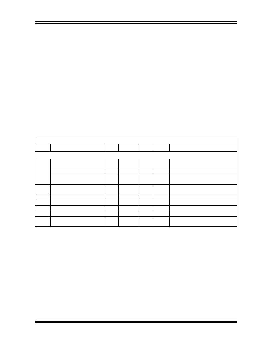
TC7136 AND TC7136A ELECTRICAL SPECIFICATIONS
Electrical Characteristics: V
S
= 9V, f
CLK
= 16kHz, and T
A
= +25∞C, unless otherwise noted.
Symbol
Parameter
Min
Typ
Max
Unit
Test Conditions
Input
Zero Input Reading
-000.0
±000.0
+000.0
Digital
Reading
V
IN
= 0V, Full Scale = 200mV
Zero Reading Drift
--
0.2
1
µ
V/∞C
V
IN
= 0V, 0∞C
T
A
+70∞C
Ratiometric Reading
999
999/1000
1000
Digital
Reading
V
IN
= V
REF
, V
REF
= 100mV
NL
Non-Linearity Error
--
1
±0.2
Count
Full Scale = 20mV or 2V Max.
Deviation from best Straight Line
E
R
Rollover Error
-1
-1
±0.2
1 Count
V
IN
- = V
IN
+
200mV
e
N
Noise
--
15
--
µ
V
P-P
V
IN
= 0V, Full Scale = 200mV
I
L
Input Leakage Current
--
1
10
pA
V
IN
= 0V
CMRR
Common Mode Rejection Ratio
--
50
--
µ
V/V
V
CM
= ±1V, V
IN
= 0V, Full Scale = 200mV
TC
SF
Scale Factor Temperature
Coefficient
--
1
5
ppm/∞C
V
IN
= 199mV, 0∞C
T
A
+70∞C
Ext. Ref. Temp. Coeff. = 0ppm/∞C
Note
1:
Input voltages may exceed supply voltages when input current is limited to 100
µ
A.
2:
Dissipation rating assumes device is mounted with all leads soldered to PC board.
3:
Refer to "Differential Input" discussion.
4:
Backplane drive is in phase with segment drive for "OFF" segment and 180∞ out-of-phase for "ON" segment. Frequency
is 20 times conversion rate. Average DC component is less than 50mV.
5:
See "Typical Application".
6:
A 48kHz oscillator increases current by 20
µ
A (typical). Common current not included.


