21461b.book
©
2002 Microchip Technology Inc.
DS21461B-page 1
TC7136/TC7136A
Features
· Fast Over Range Recovery, Ensured First Reading
Accuracy
· Low Temperature Drift Internal Reference
- TC7136: 70ppm/°C (Typ.)
- TC7136A: 35ppm/°C (Typ.)
· Zero Reading with Zero Input
· Low Noise: 15
µ
V
P-P
· High Resolution: 0.05%
· Low Input Leakage Current: 1pA (Typ.)/10pA (Max.)
· Precision Null Detectors with True Polarity at Zero
· High-Impedance Differential Input
· Convenient 9V Battery Operation with Low Power
Dissipation: 500
µ
W (Typ.)/900
µ
W (Max.)
Applications
· Thermometry
· Bridge Readouts: Strain Gauges, Load Cells,
Null Detectors
· Digital Meters: Voltage/Current/Ohms/Power, pH
· Digital Scales, Process Monitors
· Portable Instrumentation
Device Selection Table
General Description
The TC7136 and TC7136A are low power, 3-1/2 digit
with liquid crystal display (LCD) drivers and analog-to-
digital converters. These devices incorporate an "inte-
grator output zero" phase, which enables over range
recovery.
The
performance
of
existing
TC7126,
TC7126A and ICL7126 based systems may be
upgraded with minor changes to external, passive
components.
The TC7136A has an improved internal zener refer-
ence voltage circuit which maintains the analog com-
mon temperature drift to 35ppm/°C (typical) and
75ppm/°C (maximum). This represents an improve-
ment of two to four times over similar 3-1/2 digit con-
verters.
The
costly,
space
consuming
external
reference source may be removed.
The TC7136 and TC7136A limit linearity error to less
than 1 count on 200mV or 2V full scale ranges. The roll-
over error (the difference in readings for equal magni-
tude, but opposite polarity input signals) is below ±1
count. High-impedance differential inputs offer 1pA
leakage currents and a 10
12
input impedance. The
differential reference input allows ratiometric measure-
ments for ohms or bridge transducer measurements.
The 15
µ
V
P-P
noise performance ensures a "rock solid"
reading. The auto-zero cycle enables a zero display
readout for a 0V input.
Part Number
Package
Temperature
Range
TC7136 CPI
40-Pin PDIP
0
°
C to +70
°
C
TC7136 CKW
44-Pin PQFP
0
°
C to +70
°
C
TC7136 CLW
44-Pin PLCC
0
°
C to +70
°
C
TC7136A CPI
40-Pin PDIP
0
°
C to +70
°
C
TC7136A CKW
44-Pin PQFP
0
°
C to +70
°
C
TC7136A CLW
44-Pin PLCC
0
°
C to +70
°
C
Low Power 3-1/2 Digit Analog-to-Digital Converter
TC7136/TC7136A
DS21461B-page 2
©
2002 Microchip Technology Inc.
Package Type
TC7136CPL
TC7136ACPL
1
2
3
4
OSC1
5
6
7
8
9
10
11
12
TEST
V
REF
+
ANALOG
COMMON
C
AZ
V+
D
2
Normal Pin
Configuration
13
14
15
16
17
18
19
20
40
39
38
37
36
35
34
33
32
31
30
29
28
27
26
25
24
23
22
21
C
2
B
2
A
2
F
2
E
2
D
3
B
3
F
3
E
3
AB
4
10's
100's
1000's
100's
OSC2
OSC3
V
REF
-
C
REF
+
C
REF
-
V
IN
+
V
IN
-
V
BUFF
V
INT
V-
G
2
C
3
A
3
G
3
BP
(Backplane)
POL
(MINUS SIGN)
TC7136RCPL
TC7136ARCPL
1
2
3
4
5
6
7
8
9
10
11
12
13
14
15
16
17
18
19
20
100's
1000's
100's
Reverse Pin
Configuration
40
39
38
37
36
35
34
33
32
31
30
29
28
27
26
25
24
23
22
21
D
1
C
1
B
1
A
1
F
1
G
1
E
1
1's
V+
D
2
C
2
B
2
A
2
F
2
E
2
D
3
B
3
F
3
E
3
AB
4
POL
(Minus Sign)
D
1
C
1
B
1
A
1
F
1
G
1
E
1
1's
10's
OSC1
TEST
V
REF
+
ANALOG
COMMON
C
AZ
OSC2
OSC3
V
REF
-
C
REF
+
C
REF
-
V
IN
+
V
IN
-
V
BUFF
V
INT
V-
G
2
C
3
A
3
G
3
BP
(Backplane)
NC = No Internal Connection
27
28
29
30
31
32
33
7
4
3
2
1
NC
TC7136CKW
TC7136ACKW
12
13
14
15
17
18
G
2
44
43
42
41
39
38
40
REF HI
ANALOG COMMON
16
37
AZ
36
B
UFF
35
INT
34
V-
19
20
21
22
D
3
26
8
25
9
24
10
23
11
IN HI
5
6
C
3
OSC3
TEST
NC
NC
V+
D
2
C
2
B
2
A
2
F
2
E
2
NC
OSC2
OSC1
REF LO
C
REF
+
C
REF
-
IN LO
A
3
G
3
BP
POL
AB
4
E
3
F
3
B
3
33
34
35
36
37
38
39
13
10
9
8
7
ANALOG
COMMON
REF LO
18
19
20
21
23
24
AB
4
POL
NC
BP
IN HI
NC
IN LO
B
2
6
5
4
3
1
44
2
A
1
OSC1
22
43
OSC2
42
OSC3
41
TEST
40
REF HI
25
26
27
28
F
3
E
3
G
3
A
3
C
3
G
2
32
14
AZ
31
15
BUFF
30
16
INT
E
2
29
17
D
3
NC
11
12
NC
C
2
D
2
F
2
A
2
B
3
TC7136CLW
TC7136ACLW
44-Pin PLCC
40-Pin PDIP
44-Pin PQFP
40-Pin PDIP
V-
B
1
C
1
D
1
V+
F
1
G
1
E
1
D
1
C
1
B
1
A
1
F
1
G
1
E
1
C
REF
+
C
REF
-
©
2002 Microchip Technology Inc.
DS21461B-page 3
TC7136/TC7136A
Typical Application
V
REF
+
TC7136
TC7136A
33
34
240k
10k
31
29
39
38
40
V
REF
-
0.47
µF
0.1
µF
V-
OSC1
OSC3
OSC2
To Analog Common (Pin 32)
1 Conversion/Sec
C
OSC
560k
180k
0.15
µF
0.01
µF
Analog
Input
+
C
REF
-
C
REF
+
V
IN
+
V
IN
-
ANALOG
COMMON
V
INT
V
BUFF
C
AZ
20
21
1
Segment
Drive
9-19
22-25
POL
BP
V+
Minus Sign
Backplane
28
50pF
LCD
1M
27
30
32
35
36
9V
+
R
OSC
26
TC7136/TC7136A
DS21461B-page 4
©
2002 Microchip Technology Inc.
Functional Block Diagram
TC7136/A
Thousands
Hundreds
Tens
Units
4
39
OSC2
V+
TES
T
1
To Switch
Clock
7-Segment
Decode
40
38
OSC3
OSC1
÷
Control Logic
26
500
Data Latch
C
REF
-
R
INT
V
C
AZ
V
INT
28
29
27
33
36
34
10
µ
A
31
ZI & AZ
INT
AZ & DE (±)
32
INT
26
Integrator
To Digital
Section
DE (+)
DE
(
)
DE
(+)
DE (
)
ANALOG
COMMON
C
REF
+
V
IN
+
V
IN
-
V
BUFF
C
INT
V
REF
+V
REF
-
ZI &
AZ
C
REF
+
35
+
LCD Segment Drivers
÷
200
BP
F
OSC
V-
V
TH
= 1V
V-
+
Internal Digital Ground
LOW
TEMPCO
V
REF
Comparator
AZ
ZI
V+
2.8V
1
R
OSC
C
OSC
7-Segment
Decode
7-Segment
Decode
21
Typical Segment Input
Internal Digital Ground
Segment
Output
V+
0.5mA
2mA
6.2V
LCD
+
37
©
2002 Microchip Technology Inc.
DS21461B-page 5
TC7136/TC7136A
1.0
ELECTRICAL
CHARACTERISTICS
Absolute Maximum Ratings*
Supply Voltage (V+ to V-) ....................................... 15V
Analog Input Voltage (Either Input) (Note 1)... V+ to V-
Reference Input Voltage (Either Input)............ V+ to V-
Clock Input .................................................TEST to V+
Package Power Dissipation (T
A
70°C) (Note 2):
Plastic DIP ................................................... 1.23W
Plastic Quad Flat Package .......................... 1.00W
PLCC ........................................................... 1.23W
Operating Temperature Range:
C Devices.......................................... 0°C to +70°C
I Devices ........................................ -25°C to +85°C
Storage Temperature Range .............. -65°C to +150°C
*Stresses above those listed under "Absolute Maximum
Ratings" may cause permanent damage to the device. These
are stress ratings only and functional operation of the device
at these or any other conditions above those indicated in the
operation sections of the specifications is not implied.
Exposure to Absolute Maximum Rating conditions for
extended periods may affect device reliability.
TC7136 AND TC7136A ELECTRICAL SPECIFICATIONS
Electrical Characteristics: V
S
= 9V, f
CLK
= 16kHz, and T
A
= +25°C, unless otherwise noted.
Symbol
Parameter
Min
Typ
Max
Unit
Test Conditions
Input
Zero Input Reading
-000.0
±000.0
+000.0
Digital
Reading
V
IN
= 0V, Full Scale = 200mV
Zero Reading Drift
--
0.2
1
µ
V/°C
V
IN
= 0V, 0°C
T
A
+70°C
Ratiometric Reading
999
999/1000
1000
Digital
Reading
V
IN
= V
REF
, V
REF
= 100mV
NL
Non-Linearity Error
--
1
±0.2
Count
Full Scale = 20mV or 2V Max.
Deviation from best Straight Line
E
R
Rollover Error
-1
-1
±0.2
1 Count
V
IN
- = V
IN
+
200mV
e
N
Noise
--
15
--
µ
V
P-P
V
IN
= 0V, Full Scale = 200mV
I
L
Input Leakage Current
--
1
10
pA
V
IN
= 0V
CMRR
Common Mode Rejection Ratio
--
50
--
µ
V/V
V
CM
= ±1V, V
IN
= 0V, Full Scale = 200mV
TC
SF
Scale Factor Temperature
Coefficient
--
1
5
ppm/°C
V
IN
= 199mV, 0°C
T
A
+70°C
Ext. Ref. Temp. Coeff. = 0ppm/°C
Note
1:
Input voltages may exceed supply voltages when input current is limited to 100
µ
A.
2:
Dissipation rating assumes device is mounted with all leads soldered to PC board.
3:
Refer to "Differential Input" discussion.
4:
Backplane drive is in phase with segment drive for "OFF" segment and 180° out-of-phase for "ON" segment. Frequency
is 20 times conversion rate. Average DC component is less than 50mV.
5:
See "Typical Application".
6:
A 48kHz oscillator increases current by 20
µ
A (typical). Common current not included.
TC7136/TC7136A
DS21461B-page 6
©
2002 Microchip Technology Inc.
Analog Common
V
CTC
Analog Common Temperature
Coefficient
250k
between Common and V+
TC7136A
--
35
75
ppm/°C
0°C
T
A
+70°C
TC7136
--
70
150
ppm/°C
"C" Commercial Temp. Range Devices
TC7136A
--
35
100
ppm/°C
-25°C
T
A
+85°C
TC7136
--
70
150
ppm/°C
"I" Industrial Temp. Range Devices
V
C
Analog Common Voltage
2.7
3.05
3.35
V
250k
Between Common and V+
LCD Drive
V
SD
LCD Segment Drive Voltage
4
5
6
V
P-P
V+ to V- = 9V
V
BD
LCD Backplane Drive Voltage
4
5
6
V
P-P
V+ to V- = 9V
Power Supply
I
S
Power Supply Current
--
70
100
µ
A
V
IN
= 0V, V+ to V- = 9V (Note 6)
TC7136 AND TC7136A ELECTRICAL SPECIFICATIONS (CONTINUED)
Electrical Characteristics: V
S
= 9V, f
CLK
= 16kHz, and T
A
= +25°C, unless otherwise noted.
Symbol
Parameter
Min
Typ
Max
Unit
Test Conditions
Note
1:
Input voltages may exceed supply voltages when input current is limited to 100
µ
A.
2:
Dissipation rating assumes device is mounted with all leads soldered to PC board.
3:
Refer to "Differential Input" discussion.
4:
Backplane drive is in phase with segment drive for "OFF" segment and 180° out-of-phase for "ON" segment. Frequency
is 20 times conversion rate. Average DC component is less than 50mV.
5:
See "Typical Application".
6:
A 48kHz oscillator increases current by 20
µ
A (typical). Common current not included.
©
2002 Microchip Technology Inc.
DS21461B-page 7
TC7136/TC7136A
2.0
PIN DESCRIPTIONS
The descriptions of the pins are listed in Table 2-1.
TABLE 2-1:
PIN DESCRIPTION
Pin Number
(40-Pin PDIP)
Normal
(Reverse)
Symbol
Description
1
(40)
V+
Positive supply voltage.
2
(39)
D
1
Activates the D section of the units display.
3
(38)
C
1
Activates the C section of the units display.
4
(37)
B
1
Activates the B section of the units display.
5
(36)
A
1
Activates the A section of the units display.
6
(35)
F
1
Activates the F section of the units display.
7
(34)
G
1
Activates the G section of the units display.
8
(33)
E
1
Activates the E section of the units display.
9
(32)
D
2
Activates the D section of the tens display.
10
(31)
C
2
Activates the C section of the tens display.
11
(30)
B
2
Activates the B section of the tens display.
12
(29)
A
2
Activates the A section of the tens display.
13
(28)
F
2
Activates the F section of the tens display.
14
(27)
E
2
Activates the E section of the tens display.
15
(26)
D
3
Activates the D section of the hundreds display.
16
(25)
B
3
Activates the B section of the hundreds display.
17
(24)
F
3
Activates the F section of the hundreds display.
18
(23)
E
3
Activates the E section of the hundreds display.
19
(22)
AB
4
Activates both halves of the 1 in the thousands display.
20
(21)
POL
Activates the negative polarity display.
21
(20)
BP
Backplane drive output.
22
(19)
G
3
Activates the G section of the hundreds display.
23
(18)
A
3
Activates the A section of the hundreds display.
24
(17)
C
3
Activates the C section of the hundreds display.
25
(16)
G
2
Activates the G section of the tens display.
26
(15)
V-
Negative power supply voltage.
27
(14)
V
INT
The integrating capacitor should be selected to give the maximum voltage swing
that ensures component tolerance buildup will not allow the integrator output to sat-
urate. When analog common is used as a reference and the conversion rate is 3
readings per second, a 0.047
µ
F capacitor may be used. The capacitor must have a
low dielectric constant to prevent rollover errors. See Section 6.3, Integrating
Capacitor for additional details.
28
(13)
V
BUFF
Integration resistor connection. Use a 180k
for a 20mV full scale range and a
1.8M
for 2V full scale range.
29
(12)
C
AZ
The size of the auto-zero capacitor influences the system noise. Use a 0.47
µ
F
capacitor for a 200mV full scale and a 0.1
µ
F capacitor for a 2V full scale.
See Section 6.1, Auto-Zero Capacitor for more details.
30
(11)
V
IN
-
The low input signal is connected to this pin.
31
(10)
V
IN
+
The high input signal is connected to this pin.
32
(9)
ANALOG
COMMON
This pin is primarily used to set the Analog Common mode voltage for battery
operation, or in systems where the input signal is referenced to the power supply.
See Section 7.3, Analog Common for more details. It also acts as a reference
voltage source.
33
(8)
C
REF
-
See Pin 34.
TC7136/TC7136A
DS21461B-page 8
©
2002 Microchip Technology Inc.
34
(7)
C
REF
+
A 0.1
µ
F capacitor is used in most applications. If a large Common mode voltage
exists (for example, the V
IN
- pin is not at analog common) and a 200mV scale is
used, a 1
µ
F capacitor is recommended, which will hold the rollover error to
0.5 count.
35
(6)
V
REF
-
See Pin 36.
(5)
V
REF
+
The analog input required to generate a full scale output (1999 counts). Place
100mV between Pins 35 and 36 for 199.9mV full scale. Place 1V between Pins 35
and 36 for 2V full scale. See Section 6.6, Reference Voltage.
36
(4)
TEST
Lamp test. When pulled HIGH (to V+), all segments will be turned ON and the
display should read
-1888
. It may also be used as a negative supply for externally
generated decimal points. See Section 7.4, Test for additional information.
37
(3)
OSC3
See Pin 40.
38
(2)
OSC2
See Pin 40.
39
(1)
OSC1
Pins 40, 39 and 38 make up the oscillator section. For a 48kHz clock
(3 readings per second), connect Pin 40 to the junction of a 180k
resistor and a
50pF capacitor. The 180k
resistor is tied to Pin 39 and the 50pF capacitor is tied
to Pin 38.
TABLE 2-1:
PIN DESCRIPTION (CONTINUED)
Pin Number
(40-Pin PDIP)
Normal
(Reverse)
Symbol
Description
©
2002 Microchip Technology Inc.
DS21461B-page 9
TC7136/TC7136A
3.0
DETAILED DESCRIPTION
(All Pin Designations Refer to 40-Pin PDIP.)
3.1
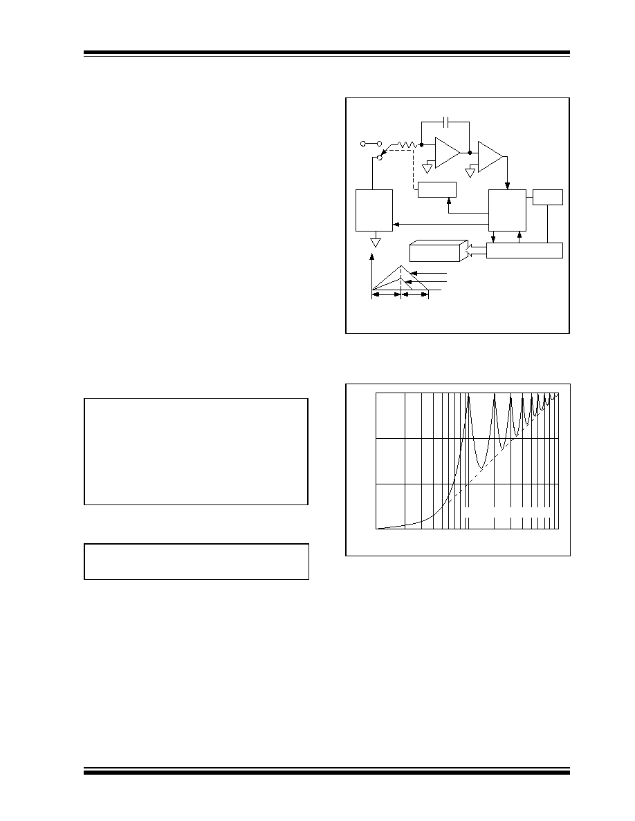
Dual Slope Conversion Principles
The TC7136/A is a dual slope, integrating analog-to-
digital converter. An understanding of the dual slope
conversion technique will aid in following detailed
TC7136/A operational theory.
The conventional dual slope converter measurement
cycle has two distinct phases (see Figure 3-1).
1.
Input signal integration
2.
Reference voltage integration (de-integration)
The input signal being converted is integrated for a
fixed time period (t
SI
), measured by counting clock
pulses. An opposite polarity constant reference voltage
is then integrated until the integrator output voltage
returns to zero. The reference integration time is
directly proportional to the input signal (t
RI
).
In a simple dual slope converter, a complete conver-
sion requires the integrator output to "ramp up" and
"ramp down."
A simple mathematical equation relates the input
signal, reference voltage, and integration time:
EQUATION 3-1:
For a constant V
IN
:
EQUATION 3-2:
FIGURE 3-1:
BASIC DUAL SLOPE
CONVERTER
FIGURE 3-2:
NORMAL MODE
REJECTION OF DUAL
SLOPE CONVERTER
The dual slope converter accuracy is unrelated to the
integrating resistor and capacitor values, as long as
they are stable during a measurement cycle. Noise
immunity is an inherent benefit. Noise spikes are inte-
grated or averaged to zero during integration periods.
Integrating ADCs are immune to the large conversion
errors that plague successive approximation convert-
ers in high noise environments. Interfering signals with
frequency components at multiples of the averaging
period will be attenuated. Integrating ADCs commonly
operate with the signal integration period set to a
multiple of the 50Hz/60Hz power line period.
1
RC
---------
V
IN
t
( )
t
d
0
t
SI
V
R
t
RI
RC
------------
=
Where:
V
R
= Reference voltage
t
SI
= Signal integration time (fixed)
t
RI
= Reference voltage integration time
(variable)
V
IN
V
R
t
RI
t
SI
--------
=
+
REF
Voltage
Analog Input
Signal
+
Display
Switch
Driver
Control
Logic
Integrator
Output
Clock
Counter
Polarity Control
Phase
Control
V
IN
V
REF
V
IN
1/2 V
REF
Variable
Reference
Integrate
Time
Fixed
Signal
Integrate
Time
Integrator
Comparator
C
INT
30
20
10
0
Normal Mode Rejection (dB)
0.1/t
1/t
10/t
Input Frequency
t = Measured Period
TC7136/TC7136A
DS21461B-page 10
©
2002 Microchip Technology Inc.
4.0
ANALOG SECTION
In addition to the basic integrate and de-integrate dual
slope cycles discussed above, the TC7136 and
TC7136A designs incorporate an "integrator output
zero cycle" and an "auto-zero cycle." These additional
cycles ensure the integrator starts at 0V (even after a
severe over range conversion) and that all offset volt-
age errors (buffer amplifier, integrator and comparator)
are removed from the conversion. A true digital zero
reading is assured without any external adjustments.
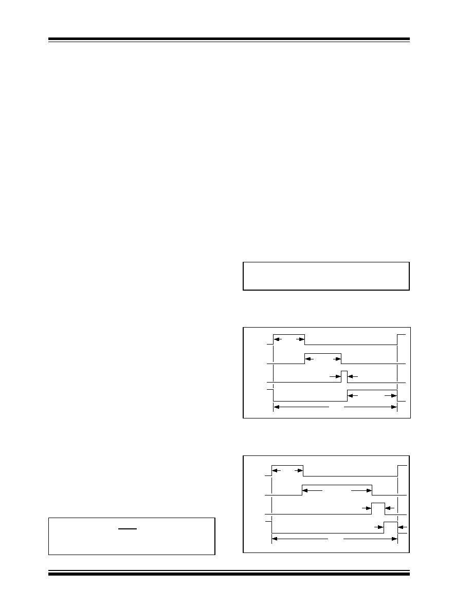
A complete conversion consists of four distinct phases:
1.
Integrator output zero phase
2.
Auto-zero phase
3.
Signal integrate phase
4.
Reference de-integrate phase
4.1
Integrator Output Zero Phase
This phase ensures the integrator output is at 0V
before the system zero phase is entered. This ensures
that true system offset voltages will be compensated
for, even after an over range conversion. The count for
this phase is a function of the number of counts
required by the de-integrate phase. The count lasts
from 11 to 140 counts for non over range conversions
and from 31 to 640 counts for over range conversions.
4.2
Auto-Zero Phase
During the auto-zero phase, the differential input signal
is disconnected from the circuit by opening internal
analog gates. The internal nodes are shorted to analog
common (ground) to establish a zero input condition.
Additional analog gates close a feedback loop around
the integrator and comparator. This loop permits com-
parator offset voltage error compensation. The voltage
level established on C
AZ
compensates for device offset
voltages. The auto-zero phase residual is typically
10
µ
V to 15
µ
V.
The auto-zero duration is from 910 to 2900 counts for
non over range conversions and from 300 to 910
counts for over range conversions.
4.3
Signal Integration Phase
The auto-zero loop is entered and the internal differen-
tial inputs connect to V
IN
+ and V
IN
-. The differential
input signal is integrated for a fixed time period. The
TC7136/A signal integration period is 1000 clock peri-
ods or counts. The externally set clock frequency is
divided by four before clocking the internal counters.
The integration time period is:
EQUATION 4-1:
The differential input voltage must be within the device
Common mode range when the converter and mea-
sured system share the same power supply common
(ground). If the converter and measured system do not
share the same power supply common, V
IN
- should be
tied to analog common.
Polarity is determined at the end of signal integrate
phase. The sign bit is a true polarity indication, in that
signals less than 1LSB are correctly determined. This
allows precision null detection, limited only by device
noise and auto-zero residual offsets.
4.4
Reference Integrate Phase
The third phase is reference integrate or de-integrate.
V
IN
- is internally connected to analog common and
V
IN
+ is connected across the previously charged refer-
ence capacitor. Circuitry within the chip ensures that
the capacitor will be connected with the correct polarity
to cause the integrator output to return to zero. The
time required for the output to return to zero is propor-
tional to the input signal and is between 0 and 2000
internal clock periods. The digital reading displayed is:
EQUATION 4-2:
FIGURE 4-1:
CONVERSION TIMING
DURING NORMAL
OPERATION
FIGURE 4-2:
CONVERSION TIMING
DURING OVER RANGE
OPERATION
t
SI
=
x 1000
4
F
OSC
Where F
OSC
= external clock frequency.
1000
V
IN
V
REF
----------------
=
INT
DENT
ZI
AZ
4000
910-2900
1-2000
1000
11-140
AZ
4000
ZI
DEINT
INT
1000
2001-2090
31-640
300-910
©
2002 Microchip Technology Inc.
DS21461B-page 11
TC7136/TC7136A
5.0
DIGITAL SECTION
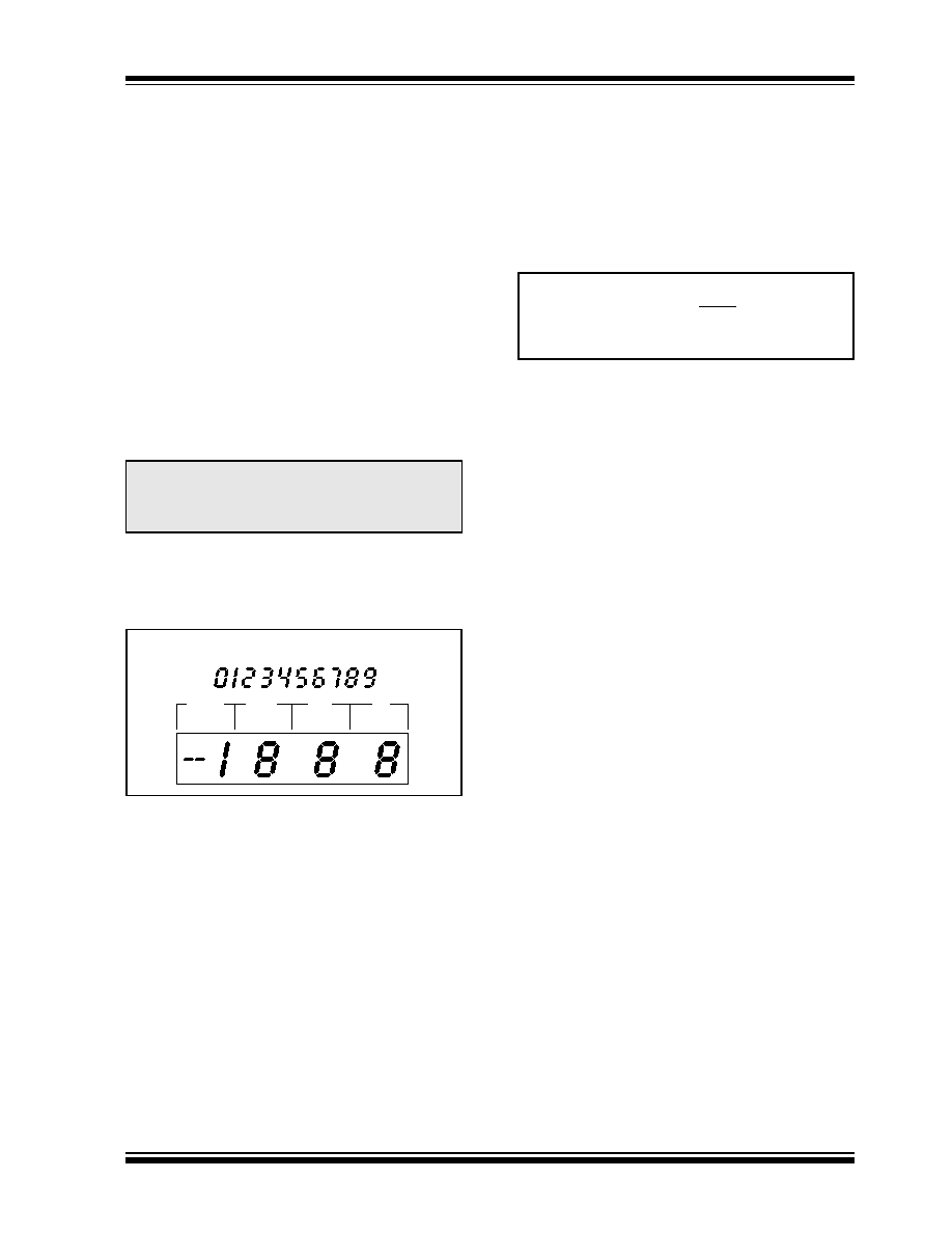
The TC7136/A contains all the segment drivers neces-
sary to directly drive a 3-1/2 digit LCD. An LCD back-
plane driver is included. The backplane frequency is
the external clock frequency divided by 800. For three
conversions per second, the backplane frequency is
60Hz with a 5V nominal amplitude. When a segment
driver is in phase with the backplane signal, the seg-
ment is OFF. An out-of-phase segment drive signal
causes the segment to be ON, or visible. This AC drive
configuration results in negligible DC voltage across
each LCD segment, ensuring long LCD life. The polar-
ity segment driver is ON for negative analog inputs. If
V
IN
+ and V
IN
- are reversed, this indicator would
reverse.
On the TC7136/A, when the TEST pin is pulled to V+,
all segments are turned ON. The display reads
-1888
.
During this mode, the LCD segments have a constant
DC voltage impressed.
The display font and segment drive assignment are
shown in Figure 5-1.
FIGURE 5-1:
DISPLAY FONT AND
SEGMENT ASSIGNMENT
5.1
System Timing
The oscillator frequency is divided by 4 prior to clocking
the internal decade counters. The four-phase mea-
surement cycle takes a total of 4000 counts, or 16,000
clock pulses. The 4000 count cycle is independent of
input signal magnitude.
Each phase of the measurement cycle has the
following length:
1.
Auto-zero phase: 3000 to 2900 counts
(1200 to 11,600 clock pulses)
2.
Signal integrate: 1000 counts
(4000 clock pulses)
This time period is fixed. The integration period is:
EQUATION 5-1:
3.
Reference integrate: 0 to 2000 counts
4.
Zero integrator: 11 to 640 counts
The TC7136 is a drop-in replacement for the TC7126
and ICL7126. The TC7136A offers a greatly improved
internal reference temperature coefficient. Minor com-
ponent value changes are required to upgrade existing
designs and improve the noise performance.
6.0
COMPONENT VALUE
SELECTION
6.1
Auto-Zero Capacitor (C
AZ
)
The C
AZ
capacitor size has some influence on system
noise. A 0.47
µ
F capacitor is recommended for 200mV
full scale applications, where 1LSB is 100
µ
V. A 0.1
µ
F
capacitor is adequate for 2V full scale applications. A
Mylar type dielectric capacitor is adequate.
6.2
Reference Voltage Capacitor
(C
REF
)
The reference voltage, used to ramp the integrator out-
put voltage back to zero during the reference integrate
phase, is stored on C
REF
. A 0.1
µ
F capacitor is accept-
able when V
REF
- is tied to analog common. If a large
Common mode voltage exists (V
REF
-
analog com-
mon) and the application requires a 200mV full scale,
increase C
REF
to 1
µ
F. Rollover error will be held to less
than 0.5 count. A Mylar type dielectric capacitor is
adequate.
6.3
Integrating Capacitor (C
INT
)
C
INT
should be selected to maximize integrator output
voltage swing without causing output saturation. Ana-
log common will normally supply the differential voltage
reference in this case, a ±2V full scale integrator output
swing is satisfactory. For 3 readings per second
(F
OSC
= 48kHz), a 0.047
µ
F value is suggested. For
one reading per second, 0.15
µ
F is recommended. If a
different oscillator frequency is used, C
INT
must be
changed in inverse proportion to maintain the nominal
±2V integrator swing.
Note:
Do not leave the display in this mode for
more than several minutes. LCDs may be
destroyed if operated with DC levels for
extended periods.
Display Font
1000's
100's
10's
1's
Where:
t
SI
= 4000
1
F
OSC
F
OSC
is the externally set clock frequency.
TC7136/TC7136A
DS21461B-page 12
©
2002 Microchip Technology Inc.
An exact expression for C
INT
is:
EQUATION 6-1:
C
INT
must have low dielectric absorption to minimize
rollover
error.
A
polypropylene
capacitor
is
recommended.
6.4
Integrating Resistor (R
INT
)
The input buffer amplifier and integrator are designed
with Class A output stages. The output stage idling cur-
rent is 6
µ
A. The integrator and buffer can supply 1
µ
A
drive currents with negligible linearity errors. R
INT
is
chosen to remain in the output stage linear drive
region, but not so large that PC board leakage currents
induce errors. For a 200mV full scale, R
INT
is 180k
. A
2V full scale requires 1.8M
(see Table 6-1).
TABLE 6-1:
Note:
F
OSC
= 48kHz (3 reading per sec).
R
OSC
= 180k
,
C
OSC
= 50pF.
6.5
Oscillator Components
C
OSC
should be 50pF. R
OSC
is selected from the
equation:
EQUATION 6-2:
Note that F
OSC
is ÷ 4 to generate the TC7136A's inter-
nal clock. The backplane drive signal is derived by
dividing F
OSC
by 800.
To achieve maximum rejection of 60Hz noise pickup,
the signal integrate period should be a multiple of
60Hz. Oscillator frequencies of 240kHz, 120kHz,
80kHz, 60kHz, 40kHz, etc. should be selected. For
50Hz rejection, oscillator frequencies of 200kHz,
100kHz, 66-2/3kHz, 50kHz, 40kHz, etc. would be suit-
able. Note that 40kHz (2.5 readings per second) will
reject both 50Hz and 60Hz.
6.6
Reference Voltage Selection
A full scale reading (2000 counts) requires the input
signal be twice the reference voltage.
Note:
*V
REF
= 2V
REF.
In some applications, a scale factor other than unity
may exist between a transducer output voltage and the
required digital reading. Assume, for example, a pres-
sure transducer output for 2000 lb/in
2
is 400mV. Rather
than dividing the input voltage by two, the reference
voltage should be set to 200mV. This permits the trans-
ducer input to be used directly. The differential refer-
ence can also be used when a digital zero reading is
required, when V
IN
is not equal to zero. This is common
in temperature measuring instrumentation. A compen-
sating offset voltage can be applied between analog
common and V
IN
-. The transducer output is connected
between V
IN
+ and analog common.
Component
Value
Nominal Full Scale Voltage
200mV
2V
C
AZ
0.47
µ
F
0.1
µ
F
R
INT
180k
1.8M
C
INT
0.047
µ
F
0.047
µ
F
(4000)
1
F
OSC
C
INT
=
V
FS
R
INT
V
INT
Where:
F
OSC
= Clock frequency at Pin 38
V
FS
= Full scale input voltage
R
INT
= Integrating resistor
V
INT
= Desired full scale integrator output swing
Required Full Scale Voltage*
V
REF
200mV
100mV
2V
1V
F
OSC
=
0.45
RC
©
2002 Microchip Technology Inc.
DS21461B-page 13
TC7136/TC7136A
7.0
DEVICE PIN FUNCTIONAL
DESCRIPTION
7.1
Differential Signal Inputs
V
IN
+ (Pin 31), V
IN
- (Pin 30)
The TC7136/A is designed with true differential inputs
and accepts input signals within the input stage Com-
mon mode voltage range (V
CM
). The typical range is
V+ 1V to V- + 1V. Common mode voltages are
removed from the system when the TC7136A operates
from a battery or floating power source (isolated from
measured system), Common mode voltage removed
in battery operation with V
IN
= analog common and V
IN
-
is
connected
to
analog
common
(V
COM
)
(see
Figure 7-1).
FIGURE 7-1:
COMMON MODE VOLTAGE REMOVED IN BATTERY OPERATION WITH
V
IN
= ANALOG COMMON
In systems where Common mode voltages exist, the
86dB Common mode rejection ratio minimizes error.
Common mode voltages do, however, affect the inte-
grator output level. A worst case condition exists if a
large positive V
CM
exists in conjunction with a full scale
negative differential signal. The negative signal drives
the integrator output positive along with V
CM
(see
Figure 7-2.) For such applications, the integrator out-
put swing can be reduced below the recommended 2V
full scale swing. The integrator output will swing within
0.3V of V+ or V- without increased linearity error.
FIGURE 7-2:
COMMON MODE
VOLTAGE REDUCES
AVAILABLE INTEGRATOR
SWING
(V
COM
V
IN
)
7.2
Differential Reference
V
REF
+ (Pin 36), V
REF
- (Pin 35)
The reference voltage can be generated anywhere
within the V+ to V- power supply range.
To prevent rollover type errors being induced by large
Common mode voltages, C
REF
should be large com-
pared to stray node capacitance. The TC7136/A offers
a significantly improved analog common temperature
coefficient. This potential provides a very stable volt-
age, suitable for use as a voltage reference. The
temperature coefficient of analog common is typically
35ppm/°C.
7.3
Analog Common (Pin 32)
The analog common pin is set at a voltage potential
approximately 3V below V+. The potential is between
2.7V and 3.35V below V+. Analog common is tied inter-
nally to an N-channel FET, capable of sinking 100
µ
A.
This FET will hold the common line at 3V below V+ if an
external load attempts to pull the common line toward
V+. Analog common source current is limited to 1
µ
A.
Analog common is, therefore, easily pulled to a more
negative voltage (i.e., below V+ 3V).
V
BUF
C
AZ
V
INT
BP
POL
Segment
Drive
OSC1
OSC3
OSC2
V-
V+
V
REF
+
V
REF
-
ANALOG
COMMON
V-
V+
V+
GND
GND
Measured
System
Power
Source
9V
LCD
TC7136
TC7136A
+
V-
V+
V-
R
I
+
V
IN
C
I
Integrator
V
I
=
[
[
V
CM
= V
IN
Input Buffer
C
I
= Integration capacitor
R
I
= Integration resistor
4000
F
OSC
t
I
= Integration time =
Where:
V
I
+
+
t
I
C
I
V
CM
TC7136/TC7136A
DS21461B-page 14
©
2002 Microchip Technology Inc.
The TC7136/A connects the internal V
IN
+ and V
IN
-
inputs to analog common during the auto-zero phase.
During the reference integrate phase, V
IN
- is connected
to analog common. If V
IN
- is not externally connected to
analog common, a Common mode voltage exists, but
is rejected by the converter's 86dB Common mode
rejection ratio. In battery operation, analog common
and V
IN
- are usually connected, removing Common
mode voltage concerns. In systems where V
IN
- is con-
nected to the power supply ground or to a given
voltage, analog common should be connected to V
IN
-.
The analog common pin serves to set the analog sec-
tion reference, or common point. The TC7136A is spe-
cifically designed to operate from a battery, or in any
measurement system where input signals are not refer-
enced (float), with respect to the TC7136A power
source. The analog common potential of V+ 3V gives
a 7V end of battery life voltage. The common potential
has a 0.001%/% voltage coefficient.
With
sufficiently
high
total
supply
voltage
(V+ V- > 7V), analog common is a very stable poten-
tial with excellent temperature stability (typically
35ppm/°C for TC7136A. This potential can be used to
generate the TC7136A's reference voltage. An external
voltage reference will be unnecessary in most cases,
because of the 35ppm/°C temperature coefficient. See
Section 7.5, TC7136A Internal Voltage Reference
discussion.
7.4
TEST (Pin 37)
The TEST pin potential is 5V less than V
+
. TEST may
be used as the negative power supply connection for
external CMOS logic. The TEST pin is tied to the inter-
nally generated negative logic supply through a 500
resistor. The TEST pin load should not be more than
1mA. See Section 8.0, Typical Applications for addi-
tional information on using TEST as a negative digital
logic supply.
If TEST is pulled high (to V+), all segments plus the
minus sign will be activated. DO NOT OPERATE IN
THIS MODE FOR MORE THAN SEVERAL MINUTES.
With TEST = V+, the LCD segments are impressed with
a DC voltage which will destroy the LCD.
7.5
TC7136A Internal Voltage
Reference
The TC7136 analog common voltage temperature sta-
bility has been significantly improved (Figure 7-3). The
"A" version of the industry standard TC7136 device
allows users to upgrade old systems and design new
systems without external voltage references. External
R and C values do not need to be changed; however,
noise performance will be improved by increasing C
AZ
(see Section 6.1, Auto-Zero Capacitor). Figure 7-4
shows analog common supplying the necessary
voltage reference for the TC7136/A.
FIGURE 7-3:
ANALOG COMMON
TEMPERATURE
COEFFICIENT
FIGURE 7-4:
TC7136A INTERNAL
VOLTAGE REFERENCE
CONNECTION
Typical
Maximum
Maximum
Typical
Typical
No Maximum
Specified
200
180
160
140
120
100
80
60
40
20
0
Analog Common Temperature
Coefficient (ppm/
°
C)
TC7136
TC7136A
ICL7136
V-
ANALOG
COMMON
TC7136
TC7136A
V
REF
+
32
35
36
26
240k
10k
V
REF
-
V
REF
1
+
9V
Set V
REF
= 1/2 V
REF
V+
©
2002 Microchip Technology Inc.
DS21461B-page 15
TC7136/TC7136A
8.0
TYPICAL APPLICATIONS
8.1
Liquid Crystal Display Sources
Several manufacturers supply standard LCDs to inter-
face with the TC7136A 3-1/2 digit analog-to-digital
converter.
Note:
Contact LCD manufacturer for full product listing/
specifications.
8.2
Decimal Point and Annunciator
Drive
The TEST pin is connected to the internally generated
digital logic supply ground through a 500
resistor. The
TEST pin may be used as the negative supply for exter-
nal CMOS gate segment drivers. LCD annunciators for
decimal points, low battery indication, or function indi-
cation may be added without adding an additional sup-
ply. No more than 1mA should be supplied by the TEST
pin; its potential is approximately 5V below V+.
8.3
Ratiometric Resistance
Measurements
The TC7136A's true differential input and differential
reference make ratiometric readings possible. In ratio-
metric operation, an unknown resistance is measured
with respect to a known standard resistance. No
accurately defined reference voltage is needed.
The unknown resistance is put in series with a known
standard and a current passed through the pair. The
voltage developed across the unknown is applied to the
input and the voltage across the known resistor applied
to the reference input. If the unknown equals the stan-
dard, the display will read 1000. The displayed reading
can be determined from the following expression:
EQUATION 8-1:
The display will over range for:
R
UNKNOWN
2 x R
STANDARD
FIGURE 8-1:
DECIMAL POINT AND
ANNUNCIATOR DRIVES
Manufac.
Address/Phone
Representative
Part Numbers*
Crystaloid
Electronics
5282 Hudson Dr.
Hudson, OH 44236
216-655-2429
C5335, H5535,
T5135, SX440
AND
720 Palomar Ave.
Sunnyvale, CA 94086
408-523-8200
FE 0201, 0501
FE 0203, 0701
FE 2201
VGI, Inc.
1800 Vernon St. Ste.2,
Roseville,
CA 95678
916-783-7878
I1048, I1126
Hamlin, Inc.
612 E. Lake St.
Lake Mills,
WI 53551
414-648-2361
00
3902, 3933, 3903
Displayed(Reading) =
R
UNKNOWN
R
STANDARD
x 1000
V+
V+
TC7136
TC7136A
V+
V+
TC7136
TC7136A
4049
4030
BP
TEST
BP
TEST
GND
GND
To LCD
Decimal Point
To LCD Backplane
To LCD
Decimal Point
Decimal
Point
Select
21
37
Multiple Decimal Point or
Annunciator Driver
Simple Inverter for Fixed Decimal Point
or Display Annunciator
TC7136/TC7136A
DS21461B-page 16
©
2002 Microchip Technology Inc.
FIGURE 8-2:
LOW PARTS COUNT
RATIOMETRIC
RESISTANCE
MEASUREMENT
FIGURE 8-3:
TEMPERATURE SENSOR
FIGURE 8-4:
POSITIVE TEMPERATURE
COEFFICIENT RESISTOR
TEMPERATURE SENSOR
V
REF
+
V
REF
-
V
IN
+
V
IN
-
ANALOG
COMMON
TC7136
TC7136A
LCD
R
STANDARD
R
UNKNOWN
V+
TC7136
TC7136A
V+
V-
V
IN
-
V
IN
+
V
REF
+
V
REF
-
COMMON
50k
R
2
160k
300k
300k
R
1
50k
1N4148
Sensor
9V
+
TC7136
TC7136A
V+
V-
V
IN
-
V
IN
+
V
REF
+
V
REF
-
COMMON
5.6k
160k
R
2
20k
1N4148
9V
R
1
20k
+
R
3
0.7%/
°C
PTC
©
2002 Microchip Technology Inc.
DS21461B-page 17
TC7136/TC7136A
9.0
PACKAGING INFORMATION
9.1
Package Marking Information
Package marking data not available at this time.
9.2
Taping Form
Component Taping Orientation for 44-Pin PQFP Devices
User Direction of Feed
PIN 1
Standard Reel Component Orientation
for TR Suffix Device
W
P
Package
Carrier Width (W)
Pitch (P)
Part Per Full Reel
Reel Size
44-Pin PQFP
24 mm
16 mm
500
13 in
Carrier Tape, Number of Components Per Reel and Reel Size
Note: Drawing does not represent total number of pins.
PIN 1
Component Taping Orientation for 44-Pin PLCC Devices
User Direction of Feed
Standard Reel Component Orientation
for TR Suffix Device
Note: Drawing does not represent total number of pins.
W
P
Package
Carrier Width (W)
Pitch (P)
Part Per Full Reel
Reel Size
44-Pin PLCC
32 mm
24 mm
500
13 in
Carrier Tape, Number of Components Per Reel and Reel Size
TC7136/TC7136A
DS21461B-page 18
©
2002 Microchip Technology Inc.
9.3
Package Dimensions
Dimensions: inches (mm)
2.065 (52.45)
2.027 (51.49)
.200 (5.08)
.140 (3.56)
.150 (3.81)
.115 (2.92)
.070 (1.78)
.045 (1.14)
.022 (0.56)
.015 (0.38)
.110 (2.79)
.090 (2.29)
.555 (14.10)
.530 (13.46)
.610 (15.49)
.590 (14.99)
.015 (0.38)
.008 (0.20)
.700 (17.78)
.610 (15.50)
.040 (1.02)
.020 (0.51)
40-Pin PDIP (Wide)
PIN 1
3
° MIN.
Dimensions: inches (mm)
.695 (17.65)
.685 (17.40)
.656 (16.66)
.650 (16.51)
.656 (16.66)
.650 (16.51)
.021 (0.53)
.013 (0.33)
.032 (0.81)
.026 (0.66)
.630 (16.00)
.591 (15.00)
.120 (3.05)
.090 (2.29)
.180 (4.57)
.165 (4.19)
.695 (17.65)
.685 (17.40)
.050 (1.27) TYP.
.020 (0.51) MIN.
PIN 1
44-Pin PLCC
©
2002 Microchip Technology Inc.
DS21461B-page 19
TC7136/TC7136A
9.3
Package Dimensions (Continued)
Dimensions: inches (mm)
.557 (14.15)
.537 (13.65)
.398 (10.10)
.390 (9.90)
.031 (0.80) TYP.
.018 (0.45)
.012 (0.30)
.398 (10.10)
.390 (9.90)
.010 (0.25) TYP.
.096 (2.45) MAX.
.557 (14.15)
.537 (13.65)
.083 (2.10)
.075 (1.90)
.041 (1.03)
.026 (0.65)
7
° MAX.
.009 (0.23)
.005 (0.13)
44-Pin PQFP
PIN 1

TC7136/TC7136A
DS21461B-page 20
©
2002 Microchip Technology Inc.
SALES AND SUPPORT
Data Sheets
Products supported by a preliminary Data Sheet may have an errata sheet describing minor operational differences and recom-
mended workarounds. To determine if an errata sheet exists for a particular device, please contact one of the following:
1.
Your local Microchip sales office
2.
The Microchip Corporate Literature Center U.S. FAX: (480) 792-7277
3.
The Microchip Worldwide Site (www.microchip.com)
Please specify which device, revision of silicon and Data Sheet (include Literature #) you are using.
New Customer Notification System
Register on our web site (www.microchip.com/cn) to receive the most current information on our products.

©
2002 Microchip Technology Inc.
DS21461B-page 21
TC7136/TC7136A
Information contained in this publication regarding device
applications and the like is intended through suggestion only
and may be superseded by updates. It is your responsibility to
ensure that your application meets with your specifications.
No representation or warranty is given and no liability is
assumed by Microchip Technology Incorporated with respect
to the accuracy or use of such information, or infringement of
patents or other intellectual property rights arising from such
use or otherwise. Use of Microchip's products as critical com-
ponents in life support systems is not authorized except with
express written approval by Microchip. No licenses are con-
veyed, implicitly or otherwise, under any intellectual property
rights.
Trademarks
The Microchip name and logo, the Microchip logo, FilterLab,
K
EE
L
OQ
, microID,
MPLAB, PIC, PICmicro, PICMASTER,
PICSTART, PRO MATE, SEEVAL and The Embedded Control
Solutions Company are registered trademarks of Microchip Tech-
nology Incorporated in the U.S.A. and other countries.
dsPIC, ECONOMONITOR, FanSense, FlexROM, fuzzyLAB,
In-Circuit Serial Programming, ICSP, ICEPIC, microPort,
Migratable Memory, MPASM, MPLIB, MPLINK, MPSIM,
MXDEV, PICC, PICDEM, PICDEM.net, rfPIC, Select Mode
and Total Endurance are trademarks of Microchip Technology
Incorporated in the U.S.A.
Serialized Quick Turn Programming (SQTP) is a service mark
of Microchip Technology Incorporated in the U.S.A.
All other trademarks mentioned herein are property of their
respective companies.
© 2002, Microchip Technology Incorporated, Printed in the
U.S.A., All Rights Reserved.
Printed on recycled paper.
Microchip received QS-9000 quality system
certification for its worldwide headquarters,
design and wafer fabrication facilities in
Chandler and Tempe, Arizona in July 1999
and Mountain View, California in March 2002.
The Company's quality system processes and
procedures are QS-9000 compliant for its
PICmicro
®
8-bit MCUs, K
EE
L
OQ
®
code hopping
devices, Serial EEPROMs, microperipherals,
non-volatile memory and analog products. In
addition, Microchip's quality system for the
design and manufacture of development
systems is ISO 9001 certified.

DS21461B-page 22
©
2002 Microchip Technology Inc.
AMERICAS
Corporate Office
2355 West Chandler Blvd.
Chandler, AZ 85224-6199
Tel: 480-792-7200 Fax: 480-792-7277
Technical Support: 480-792-7627
Web Address: http://www.microchip.com
Rocky Mountain
2355 West Chandler Blvd.
Chandler, AZ 85224-6199
Tel: 480-792-7966 Fax: 480-792-7456
Atlanta
500 Sugar Mill Road, Suite 200B
Atlanta, GA 30350
Tel: 770-640-0034 Fax: 770-640-0307
Boston
2 Lan Drive, Suite 120
Westford, MA 01886
Tel: 978-692-3848 Fax: 978-692-3821
Chicago
333 Pierce Road, Suite 180
Itasca, IL 60143
Tel: 630-285-0071 Fax: 630-285-0075
Dallas
4570 Westgrove Drive, Suite 160
Addison, TX 75001
Tel: 972-818-7423 Fax: 972-818-2924
Detroit
Tri-Atria Office Building
32255 Northwestern Highway, Suite 190
Farmington Hills, MI 48334
Tel: 248-538-2250 Fax: 248-538-2260
Kokomo
2767 S. Albright Road
Kokomo, Indiana 46902
Tel: 765-864-8360 Fax: 765-864-8387
Los Angeles
18201 Von Karman, Suite 1090
Irvine, CA 92612
Tel: 949-263-1888 Fax: 949-263-1338
New York
150 Motor Parkway, Suite 202
Hauppauge, NY 11788
Tel: 631-273-5305 Fax: 631-273-5335
San Jose
Microchip Technology Inc.
2107 North First Street, Suite 590
San Jose, CA 95131
Tel: 408-436-7950 Fax: 408-436-7955
Toronto
6285 Northam Drive, Suite 108
Mississauga, Ontario L4V 1X5, Canada
Tel: 905-673-0699 Fax: 905-673-6509
ASIA/PACIFIC
Australia
Microchip Technology Australia Pty Ltd
Suite 22, 41 Rawson Street
Epping 2121, NSW
Australia
Tel: 61-2-9868-6733 Fax: 61-2-9868-6755
China - Beijing
Microchip Technology Consulting (Shanghai)
Co., Ltd., Beijing Liaison Office
Unit 915
Bei Hai Wan Tai Bldg.
No. 6 Chaoyangmen Beidajie
Beijing, 100027, No. China
Tel: 86-10-85282100 Fax: 86-10-85282104
China - Chengdu
Microchip Technology Consulting (Shanghai)
Co., Ltd., Chengdu Liaison Office
Rm. 2401, 24th Floor,
Ming Xing Financial Tower
No. 88 TIDU Street
Chengdu 610016, China
Tel: 86-28-6766200 Fax: 86-28-6766599
China - Fuzhou
Microchip Technology Consulting (Shanghai)
Co., Ltd., Fuzhou Liaison Office
Unit 28F, World Trade Plaza
No. 71 Wusi Road
Fuzhou 350001, China
Tel: 86-591-7503506 Fax: 86-591-7503521
China - Shanghai
Microchip Technology Consulting (Shanghai)
Co., Ltd.
Room 701, Bldg. B
Far East International Plaza
No. 317 Xian Xia Road
Shanghai, 200051
Tel: 86-21-6275-5700 Fax: 86-21-6275-5060
China - Shenzhen
Microchip Technology Consulting (Shanghai)
Co., Ltd., Shenzhen Liaison Office
Rm. 1315, 13/F, Shenzhen Kerry Centre,
Renminnan Lu
Shenzhen 518001, China
Tel: 86-755-2350361 Fax: 86-755-2366086
Hong Kong
Microchip Technology Hongkong Ltd.
Unit 901-6, Tower 2, Metroplaza
223 Hing Fong Road
Kwai Fong, N.T., Hong Kong
Tel: 852-2401-1200 Fax: 852-2401-3431
India
Microchip Technology Inc.
India Liaison Office
Divyasree Chambers
1 Floor, Wing A (A3/A4)
No. 11, O'Shaugnessey Road
Bangalore, 560 025, India
Tel: 91-80-2290061 Fax: 91-80-2290062
Japan
Microchip Technology Japan K.K.
Benex S-1 6F
3-18-20, Shinyokohama
Kohoku-Ku, Yokohama-shi
Kanagawa, 222-0033, Japan
Tel: 81-45-471- 6166 Fax: 81-45-471-6122
Korea
Microchip Technology Korea
168-1, Youngbo Bldg. 3 Floor
Samsung-Dong, Kangnam-Ku
Seoul, Korea 135-882
Tel: 82-2-554-7200 Fax: 82-2-558-5934
Singapore
Microchip Technology Singapore Pte Ltd.
200 Middle Road
#07-02 Prime Centre
Singapore, 188980
Tel: 65-6334-8870 Fax: 65-6334-8850
Taiwan
Microchip Technology Taiwan
11F-3, No. 207
Tung Hua North Road
Taipei, 105, Taiwan
Tel: 886-2-2717-7175 Fax: 886-2-2545-0139
EUROPE
Denmark
Microchip Technology Nordic ApS
Regus Business Centre
Lautrup hoj 1-3
Ballerup DK-2750 Denmark
Tel: 45 4420 9895 Fax: 45 4420 9910
France
Microchip Technology SARL
Parc d'Activite du Moulin de Massy
43 Rue du Saule Trapu
Batiment A - ler Etage
91300 Massy, France
Tel: 33-1-69-53-63-20 Fax: 33-1-69-30-90-79
Germany
Microchip Technology GmbH
Gustav-Heinemann Ring 125
D-81739 Munich, Germany
Tel: 49-89-627-144 0 Fax: 49-89-627-144-44
Italy
Microchip Technology SRL
Centro Direzionale Colleoni
Palazzo Taurus 1 V. Le Colleoni 1
20041 Agrate Brianza
Milan, Italy
Tel: 39-039-65791-1 Fax: 39-039-6899883
United Kingdom
Arizona Microchip Technology Ltd.
505 Eskdale Road
Winnersh Triangle
Wokingham
Berkshire, England RG41 5TU
Tel: 44 118 921 5869 Fax: 44-118 921-5820
03/01/02
*DS21461B*
W
ORLDWIDE
S
ALES
AND
S
ERVICE