 | ÐлекÑÑоннÑй компоненÑ: TC7660H | СкаÑаÑÑ:  PDF PDF  ZIP ZIP |
Äîêóìåíòàöèÿ è îïèñàíèÿ www.docs.chipfind.ru
TC7660H-2 10/1/96
EVALUATION
KIT
AVAILABLE
TC7660H
© 2001 Microchip Technology Inc. DS21466A
HIGH FREQUENCY 7660 DC-TO-DC VOLTAGE CONVERTER
FEATURES
s
Pin Compatible with 7660, High Frequency
Performance DC-to-DC Converter
s
Low Cost, Two Low Value External Capacitors
Required ........................................................ (1.0
µ
F)
s
Converts +5V Logic Supply to
±
5V System
s
Wide Input Voltage Range .................... 1.5V to 10V
s
Voltage Conversion ........................................ 99.7%
s
Power Efficiency ................................................ 85%
s
Available in 8-Pin SOIC and 8-Pin PDIP Packages
GENERAL DESCRIPTION
The TC7660H is a pin-compatible, high frequency up-
grade to the Industry standard TC7660 charge pump volt-
age converter. It converts a +1.5V to +10V input to a
corresponding 1.5V to 10V output using only two low-
cost capacitors, eliminating inductors and their associated
cost, size and EMI.
The TC7660H operates at a frequency of 120kHz
(versus 10kHz for the TC7660), allowing the use of 1.0
µ
F
external capacitors. Oscillator frequency can be reduced
(for lower supply current applications) by connecting an
external capacitor from OSC to ground.
The TC7660H is available in 8-pin DIP and small
outline (SOIC) packages in commercial and extended
temperature ranges.
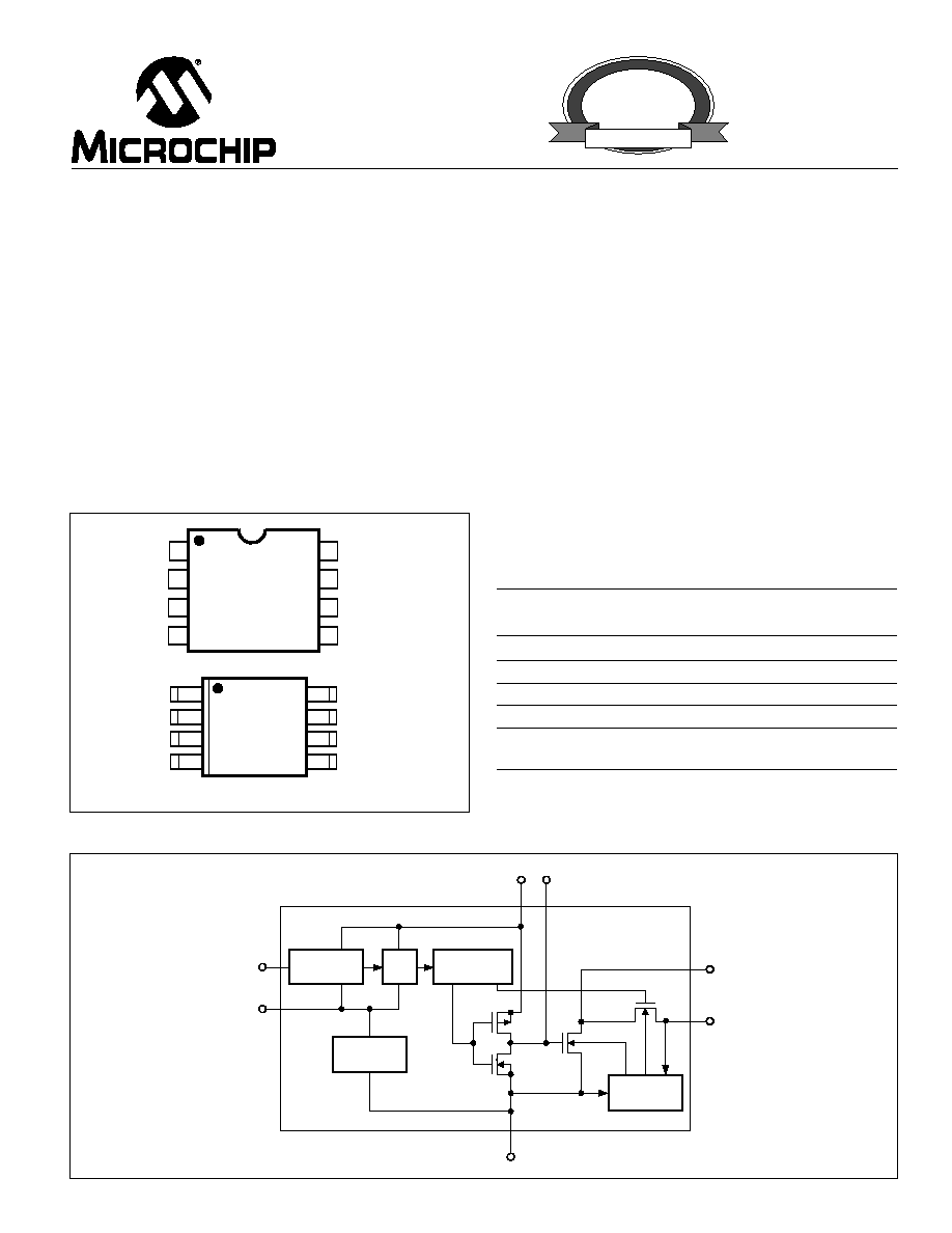
FUNCTIONAL BLOCK DIAGRAM
ORDERING INFORMATION
Temperature
Part No.
Package
Range
TC7660HCOA
8-Pin SOIC
0
°
C to +70
°
C
TC7660HCPA
8-Pin Plastic DIP
0
°
C to +70
°
C
TC7660HEOA
8-Pin SOIC
40
°
C to +85
°
C
TC7660HEPA
8-Pin Plastic DIP
40
°
C to +85
°
C
TC7660EV
Evaluation Kit for
Charge Pump Family
TC7660H
GND
INTERNAL
VOLTAGE
REGULATOR
RC
OSCILLATOR
VOLTAGE
LEVEL
TRANSLATOR
÷
2
V + CAP +
8
2
7
6
OSC
LV
3
LOGIC
NETWORK
VOUT
5
CAP
4
NC
CAP +
GND
CAP
VOUT
LOW
VOLTAGE (LV)
OSC
+
V
NC
CAP +
GND
CAP
VOUT
LOW
VOLTAGE (LV)
OSC
+
V
NC = NO INTERNAL CONNECTION
8
7
6
5
1
2
3
4
1
8
2
7
3
6
4
5
TC7660HCPA
TC7660HEPA
TC7660HCOA
TC7660HEOA
PIN CONFIGURATION (DIP and SOIC)
2
TC7660H
HIGH FREQUENCY 7660 DC-TO-DC
VOLTAGE CONVERTER
TC7660H-2 10/1/96
© 2001 Microchip Technology Inc. DS21466A
ABSOLUTE MAXIMUM RATINGS*
Supply Voltage ...................................................... +10.5V
LV and OSC Inputs
Voltage (Note 1) ........................ 0.3V to (V
+
+ 0.3V)
for V
+
< 5.5V
(V
+
5.5V) to (V
+
+ 0.3V)
for V
+
> 5.5V
Current Into LV (Note 1) ..................... 20
µ
A for V
+
> 3.5V
Output Short Duration (V
SUPPLY
5.5V) ......... Continuous
Power Dissipation (T
A
70
°
C) (Note 2)
SOIC ...............................................................470mW
Plastic DIP ...................................................... 730mW
Operating Temperature Range
C Suffix .................................................. 0
°
C to +70
°
C
E Suffix ............................................ 40
°
C to +85
°
C
Storage Temperature Range ............... 65
°
C to +150
°
C
Lead Temperature (Soldering, 10 sec) ................. +300
°
C
*Static-sensitive device. Unused devices must be stored in conductive
material. Protect devices from static discharge and static fields. Stresses
above those listed under "Absolute Maximum Ratings" may cause perma-
nent damage to the device. These are stress ratings only and functional
operation of the device at these or any other conditions above those
indicated in the operation sections of the specifications is not implied.
Exposure to absolute maximum rating conditions for extended periods may
affect device reliability.
ELECTRICAL CHARACTERISTICS:
Over Operating Temperature Range with V
+
= 5V, C
I
= C
2
= 1
µ
F, C
OSC
= 0,
Test Circuit (Figure 1), unless otherwise indicated.
Symbol
Parameter
Test Conditions
Min
Typ
Max
Unit
I
+
Supply Current
R
L
=
--
0.46
1.0
mA
V
+
H
Supply Voltage Range, High
Min
T
A
Max,
3
--
10
V
R
L
= 5k
, LV Open
V
+
L
Supply Voltage Range, Low
Min
T
A
Max,
1.5
--
3.5
V
R
L
= 5k
, LV to GND
R
OUT
Output Source Resistance
I
OUT
= 20mA, T
A
= 25
°
C
--
55
80
I
OUT
= 20mA, 0
°
C
T
A
+70
°
C
--
--
95
(C Device)
I
OUT
= 20mA, 40
°
C
T
A
+85
°
C
--
--
110
(E Device)
V
+
= 2V, I
OUT
= 3mA, LV to GND
--
150
250
0
°
C
T
A
+70
°
C
F
OSC
Oscillator Frequency
--
120
--
kHz
P
EFF
Power Efficiency
I
OUT
= 10mA, Min
T
A
Max
81
85
--
%
V
EFF
Voltage Efficiency
R
L
=
99
99.7
--
%
NOTES: 1. Connecting any input terminal to voltages greater than V+ or less than GND may cause destructive latch-up. It is recommended that no
inputs from sources operating from external supplies be applied prior to "power up" of the TC7660H.
2. Derate linearly above 50
°
C by 5.5mW/
°
C.
3
HIGH FREQUENCY 7660 DC-TO-DC
VOLTAGE CONVERTER
TC7660H
TC7660H-2 10/1/96
© 2001 Microchip Technology Inc. DS21466A
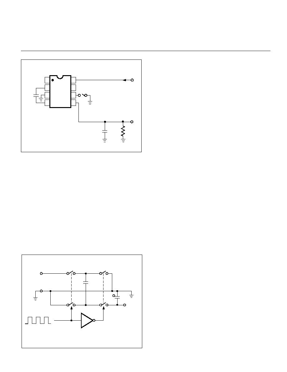
Detailed Description
The TC7660H contains all the necessary circuitry to
implement a voltage inverter, with the exception of two
external capacitors, which may be inexpensive 1.0
µ
F
non-polarized capacitors. Operation is best understood by
considering Figure 2, which shows an idealized voltage
inverter. Capacitor C
1
is charged to a voltage, V
+
, for the half
cycle when switches S
1
and S
3
are closed. (Note: Switches
S
2
and S
4
are open during this half cycle.) During the second
half cycle of operation, switches S
2
and S
4
are closed, with
S
1
and S
3
open, thereby shifting capacitor C
1
negatively by
V
+
volts. Charge is then transferred from C
1
to C
2
, such that
the voltage on C
2
is exactly V
+
, assuming ideal switches and
no load on C
2
.
V+
GND
S3
S1
S2
S4
C2
VOUT
= VIN
Figure 2. Idealized Charge Pump Inverter
Figure 1. TC7660H Test Circuit
1
2
3
4
8
7
6
5
TC7660H
+
V+
(+5V)
C1
1.0
µ
F
+
C2
1.0
µ
F
RL
IS
To improve low-voltage operation, the LV pin should be
connected to GND. For supply voltages greater than 3.5V,
the LV terminal must be left open to ensure latch-up-
proof operation and prevent device damage.
Theoretical Power Efficiency Considerations
In theory, a capacitative charge pump can approach
100% efficiency if certain conditions are met:
(1) The drive circuitry consumes minimal power.
(2) The output switches have extremely low ON
resistance and virtually no offset.
(3) The impedances of the pump and reservoir
capacitors are negligible at the pump frequency.
The TC7660H approaches these conditions for nega-
tive voltage multiplication if large values of C
1
and C
2
are
used. Energy is lost only in the transfer of charge
between capacitors if a change in voltage occurs. The
energy lost is defined by:
E = 1/2 C
1
(V
1
2
V
2
2
)
V
1
and V
2
are the voltages on C
1
during the pump and
transfer cycles. If the impedances of C
1
and C
2
are relatively
high at the pump frequency (refer to Figure 1), compared to
the value of R
L
, there will be a substantial difference in
voltages V
1
and V
2
. Therefore, it is not only desirable to
make C
2
as large as possible to eliminate output voltage
ripple, but also to employ a correspondingly large value for
C
1
in order to achieve maximum efficiency of operation.
Do's and Don'ts
· Do not exceed maximum supply voltages.
· Do not connect LV terminal to GND for supply voltages
greater than 3.5V.
· Do not short circuit the output to V
+
supply for voltages
above 5.5V for extended periods; however, transient
conditions including start-up are okay.
· When using polarized capacitors in the inverting mode,
the + terminal of C
1
must be connected to pin 2 of the
TC7660H and the + terminal of C
2
must be connected
to GND Pin 3.
4
TC7660H
HIGH FREQUENCY 7660 DC-TO-DC
VOLTAGE CONVERTER
TC7660H-2 10/1/96
© 2001 Microchip Technology Inc. DS21466A
2
2
f
C
1
X
C
= = 2.12
,
where f = 150kHz and C
1
= 1.0
µ
F.
R
OUT
(of TC7660H)
n (number of devices)
R
OUT
=
Paralleling Devices
Any number of TC7660H voltage converters may be
paralleled to reduce output resistance (Figure 4). The reser-
voir capacitor, C
2
, serves all devices, while each device
requires its own pump capacitor, C
1
. The resultant output
resistance would be approximately:
Cascading Devices
The TC7660H may be cascaded as shown in (Figure 4)
to produce larger negative multiplication of the initial supply
voltage. However, due to the finite efficiency of each device,
the practical limit is probably 10 devices for light loads. The
output voltage is defined by:
V
OUT
= n (V
IN
)
where n is an integer representing the number of devices
cascaded. The resulting output resistance would be ap-
proximately the weighted sum of the individual TC7660H
R
OUT
values.
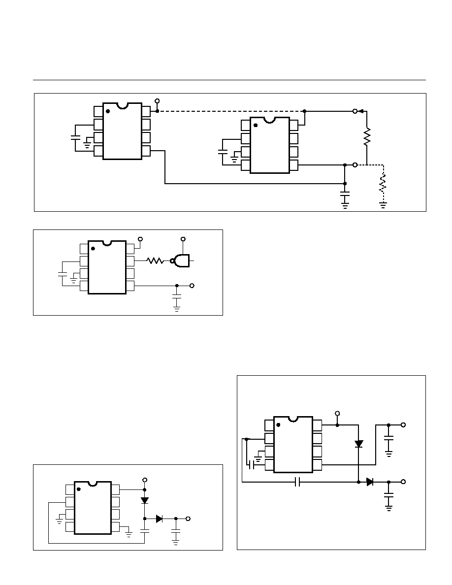
Changing the TC7660H Oscillator Frequency
It may be desirable in some applications (due to noise or
other considerations) to increase or decease the oscillator
frequency. This can be achieved by overdriving the oscilla-
tor from an external clock, as shown in Figure 6. In order to
prevent possible device latch-up, a 1k
resistor must be
used in series with the clock output. In a situation where the
designer has generated the external clock frequency using
TTL logic, the addition of a 10k
pull-up resistor to V
+
supply
is required. Note that the pump frequency with external
clocking, as with internal clocking, will be 1/2 of the clock
frequency. Output transitions occur on the positive-going
edge of the clock.
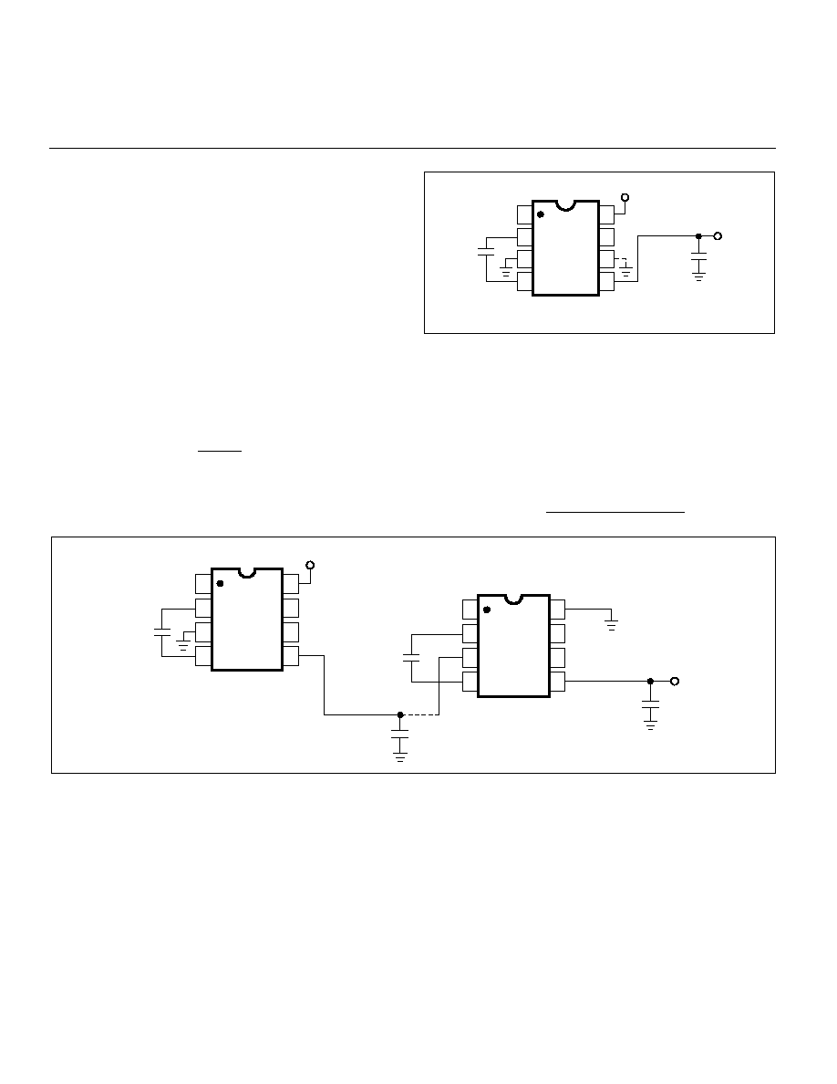
Simple Negative Voltage Converter
Figure 3 shows typical connections to provide a nega-
tive supply where a positive supply is available. A similar
scheme may be employed for supply voltages anywhere in
the operating range of +1.5V to +10V, keeping in mind that
pin 6 (LV) is tied to the supply negative (GND) only for supply
voltages below 3.5V.
The output characteristics of the circuit in Figure 3 are
those of a nearly ideal voltage source in series with 70
.
Thus, for a load current of 10 mA and a supply voltage of
+5V, the output voltage would be 4.3V.
The dynamic output impedance of the TC7660H is due,
primarily, to capacitive reactance of the charge transfer
capacitor (C
1
). Since this capacitor is connected to the
output for only 1/2 of the cycle, the equation is:
1
2
3
4
8
7
6
5
TC7660H
1.0
µ
F
+
V
+
1.0
µ
F
+
VOUT
*
1. VOUT = n V
+
for 1.5V V
+
10V
NOTES:
*
C1
C2
Figure 3. Simple Negative Converter
Figure 4. Increased Output Voltage by Cascading Devices
1
2
3
4
8
7
6
5
V
+
1
2
3
4
8
7
6
5
1.0
µ
F
1.0
µ
F
"n"
"1"
1.0
µ
F
VOUT
1. VOUT = n V
+
for 1.5V V 10V
+
NOTES:
*
*
+
+
+
TC7660H
TC7660H
5
HIGH FREQUENCY 7660 DC-TO-DC
VOLTAGE CONVERTER
TC7660H
TC7660H-2 10/1/96
© 2001 Microchip Technology Inc. DS21466A
Figure 5. Paralleling Devices Lowers Output Impedance
1
2
3
4
8
7
6
5
TC7660H
V
+
1
2
3
4
8
7
6
5
TC7660H
C1
RL
C2
C1
"n"
"1"
+
RL
1
2
3
4
8
7
6
5
TC7660H
+
V +
+
CMOS
GATE
1.0
µ
F
VOUT
1.0
µ
F
1 k
V +
Figure 6. External Clocking
Figure 7. Positive Voltage Multiplier
Positive Voltage Multiplication
The TC7660H may be employed to achieve positive
voltage multiplication using the circuit shown in Figure 7. In
this application, the pump inverter switches of the TC7660H
are used to charge C
1
to a voltage level of V
+
V
F
(where V
+
is the supply voltage and V
F
is the forward voltage drop of
diode D
1
). On the transfer cycle, the voltage on C
1
plus the
supply voltage (V
+
) is applied through diode D
2
to capacitor
C
2
. The voltage thus created on C
2
becomes (2 V
+
) (2 V
F
),
or twice the supply voltage minus the combined forward
voltage drops of diodes D
1
and D
2
.
The source impedance of the output (V
OUT
) will depend
on the output current, but for V
+
= 5V and an output current
of 10mA, it will be approximately 60
.
Combined Negative Voltage Conversion
and Positive Supply Multiplication
Figure 8 combines the functions shown in Figures 3 and
8 to provide negative voltage conversion and positive volt-
age multiplication simultaneously. This approach would be,
for example, suitable for generating +9V and 5V from an
existing +5V supply. In this instance, capacitors C
1
and C
3
perform the pump and reservoir functions, respectively, for
the generation of the negative voltage, while capacitors C
2
and C
4
are pump and reservoir, respectively, for the multi-
plied positive voltage. There is a penalty in this configuration
which combines both functions, however, in that the source
impedances of the generated supplies will be somewhat
higher due to the finite impedance of the common charge
pump driver at pin 2 of the device.
1
2
3
4
8
7
6
5
+
V +
VOUT =
(2 V +) (2 VF)
C1
D1
+
+
C3
C4
VOUT =
(V+ VF)
C2
TC7660H
D2
+
Figure 8. Combined Negative Converter and Positive Multiplier
1
2
3
4
8
7
6
5
V+
VOUT =
(2 V+) (2 VF)
+
C2
D1
D2
+
C1
TC7660H