TC7662A
EVALUATION
KIT
AVAILABLE
TC7662A-5 9/11/96
© 2001 Microchip Technology Inc. DS21468
+
COMPARATOR
WITH HYSTERESIS
C
F/F
Q
Q
VREF
LEVEL
SHIFT
LEVEL
SHIFT
LEVEL
SHIFT
LEVEL
SHIFT
VDD
P SW1
CAP
CP
EXT
N SW4
N SW2
N SW3
CAP
CR
EXT
RL
V
I
COSC
+
GND
OUT
8
2
3
OUT
5
4
7
+
+
TC7662A
GENERAL DESCRIPTION
The TC7662A is a pin-compatible upgrade to the In-
dustry standard TC7660 charge pump voltage converter. It
converts a +3V to +18V input to a corresponding 3V to
18V output using only two low-cost capacitors, eliminating
inductors and their associated cost, size and EMI. In addi-
tion to a wider power supply input range (3V to 18V versus
1.5V to 10V for the TC7660), the TC7662A can source
output currents as high as 40mA. The on-board oscillator
operates at a nominal frequency of 12kHz. Operation be-
low 10kHz (for lower supply current applications) is also
possible by connecting an external capacitor from OSC to
ground.
The TC7662A directly is recommended for designs
requiring greater output current and/or lower input/output
voltage drop. It is available in 8-pin PDIP, and CerDIP
packages in commercial and extended temperature ranges.
FEATURES
s
Wide Operating Range ............................. 3V to 18V
s
Increased Output Current .............................. 40mA
s
Pin Compatible with ICL7662/SI7661/TC7660/
LTC1044
s
No External Diodes Required
s
Low Output Impedance @ I
L
= 20mA ....... 40
Typ.
s
No Low-Voltage Terminal Required
s
CMOS Construction
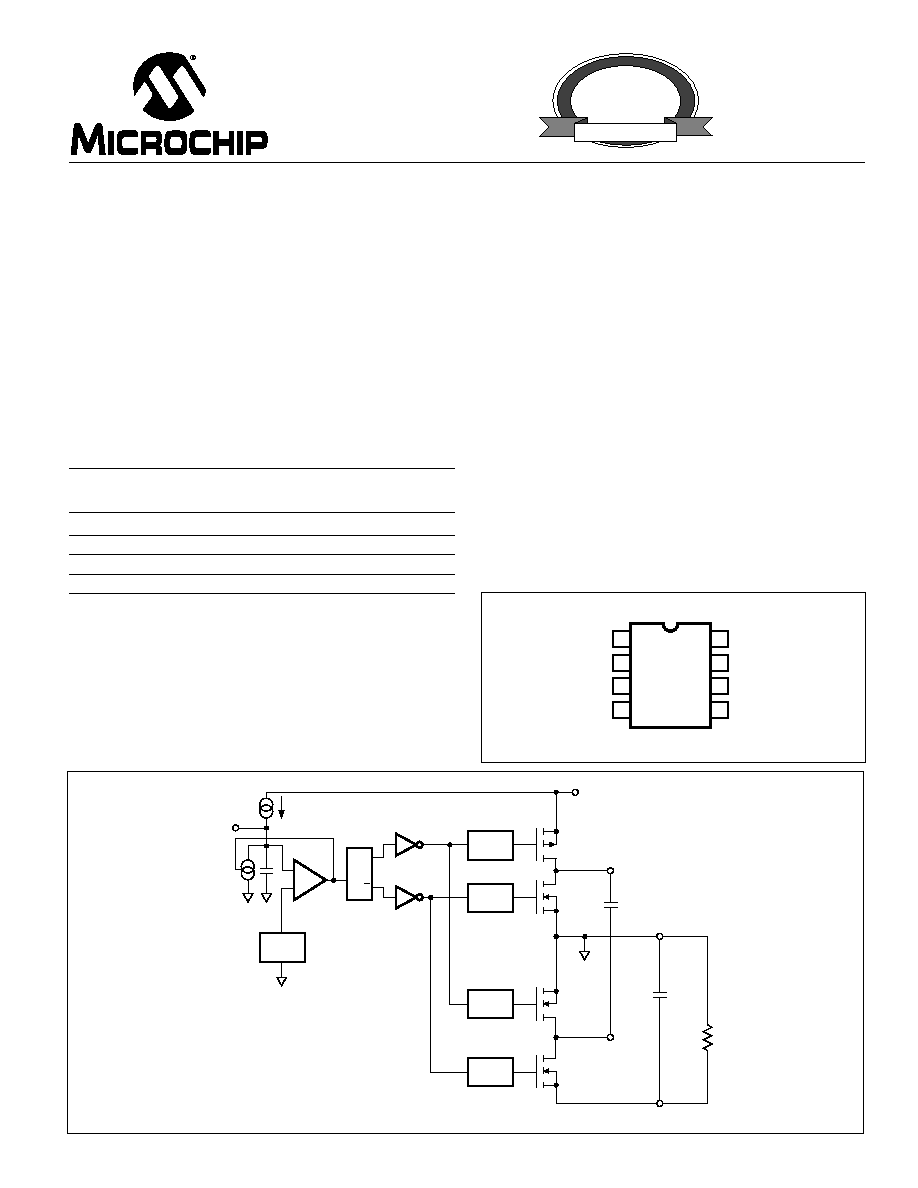
FUNCTIONAL BLOCK DIAGRAM
CHARGE PUMP DC-TO-DC CONVERTER
ORDERING INFORMATION
Temperature
Part No.
Package
Range
TC7662ACPA
8-Pin Plastic DIP
0
°
C to +70
°
C
TC7662AEPA
8-Pin Plastic DIP
40
°
C to +85
°
C
TC7662AIJA
8-Pin CerDIP
25
°
C to +85
°
C
TC7662AMJA
8-Pin CerDIP
55
°
C to +125
°
C
TC7662A
1
2
3
4
V
DD
5
6
7
8
OSC
V
OUT
NC
C
+
GND
C
NC
NC = NO INTERNAL CONNECTION
PIN CONFIGURATION
PDIP/CerDIP

2
CHARGE PUMP DC-TO-DC CONVERTER
TC7662A
TC7662A-5 9/11/96
© 2001 Microchip Technology Inc. DS21468
ABSOLUTE MAXIMUM RATINGS*
Supply Voltage V
DD
to GND .................................... +18V
Input Voltage (Any Pin) ........... (V
DD
+ 0.3) to (V
SS
0.3)
Current Into Any Pin ................................................. 10mA
Operating Temperature Range
C Suffix .................................................. 0
°
C to +70
°
C
I Suffix .............................................. 25
°
C to +85
°
C
E Suffix ............................................. 40
°
C to +85
°
C
M Suffix .......................................... 55
°
C to +125
°
C
Power Dissipation (T
A
70
°
C)
Plastic DIP ...................................................... 730mW
CerDIP ........................................................... 800mW
SOIC ...........................................................................
Package Thermal Resistance
CPA, EPA
JA
.............................................. 140
°
C/W
IJA, MJA
JA
.................................................. 90
°
C/W
Storage Temperature Range ................ 65
°
C to +150
°
C
Lead Temperature (Soldering, 10 sec) ................. +300
°
C
ESD Protection ......................................................
±
2000V
Output Short Circuit ................. Continuous (at 5.5V Input)
* Static-sensitive device. Unused devices must be stored in conductive
material. Protect devices from static discharge and static fields. Stresses
above those listed under Absolute Maximum Ratings may cause perma-
nent damage to the device. These are stress ratings only and functional
operation of the device at these or any other conditions above those
indicated in the operational sections of the specifications is not implied.
Exposure to Absolute Maximum Rating Conditions for extended periods
may affect device reliability.
ELECTRICAL CHARACTERISTICS:
V
DD
= 15V, T
A
= +25
°
C (See Test Circuit), unless otherwise specified.
Symbol
Parameter
Test Conditions
Min
Typ
Max
Unit
V
DD
Supply Voltage
3
--
18
V
I
S
Supply Current
R
L
=
V
DD
= +15V
--
510
700
µ
A
0
°
C
T
A
+70
°
C
--
560
--
55
°
C
T
A
+125
°
C
--
650
--
V
DD
= +5V
--
190
--
0
°
C
T
A
+70
°
C
--
210
--
55
°
C
T
A
+125
°
C
--
210
--
R
O
Output Source
I
L
= 20mA, V
DD
= +15V
--
40
50
Resistance
I
L
= 40mA, V
DD
= +15V
--
50
60
I
L
= 3mA, V
DD
= +5V
--
100
125
C
OSC
Oscillator Frequency
--
12
--
kHz
P
EFF
Power Efficiency
V
DD
= +15V
93
97
--
%
R
L
= 2 k
V
EFF
Voltage Efficiency
V
DD
= +15V
99
99.9
--
%
R
L
=
Over Operating Temperature Range
96
--
--
3
CHARGE PUMP DC-TO-DC CONVERTER
TC7662A
TC7662A-5 9/11/96
© 2001 Microchip Technology Inc. DS21468
Note one of its characteristics is ESR (equivalent series
resistance). This parasitic resistance winds up in series with
the load. Thus, both voltage and power conversion effi-
ciency are compromised if a low ESR capacitor is not used.
For example, in the "Test Circuit", changing C
P
and C
R
capacitors from typical ESR to low ESR types, the effective
converter output impedance changed from 45
to 40
, an
improvement of 12%.
This applies to all types of capacitors, including film
types (polyester, polycarbonate etc.).
Some applications information suggests that the ca-
pacitor is not critical and attributes the limiting factor to the
capacitor's reactance value. Let's examine this:
where DS (duty cycle) = 50%.
Thus, Z
C
1.33
at f = 12kHz, where C = 10
µ
F.
For the TC7662A, f = 12,000Hz, and a typical value of
C would be 10
µ
F. This is a reactive impedance of
1.33
.
If the ESR is as great as 5
, the reactive value is not as
critical as it would first appear, since the ESR would dominate.
The 5
value is typical of a general-purpose electrolytic
capacitor.
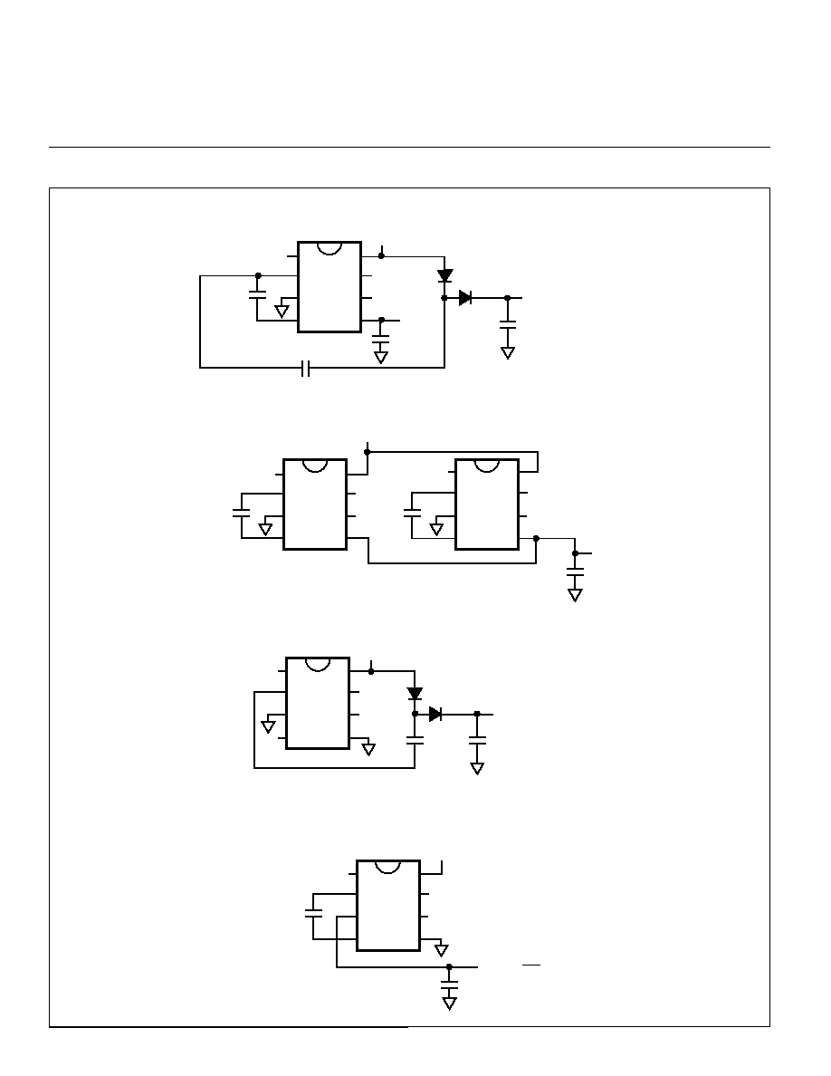
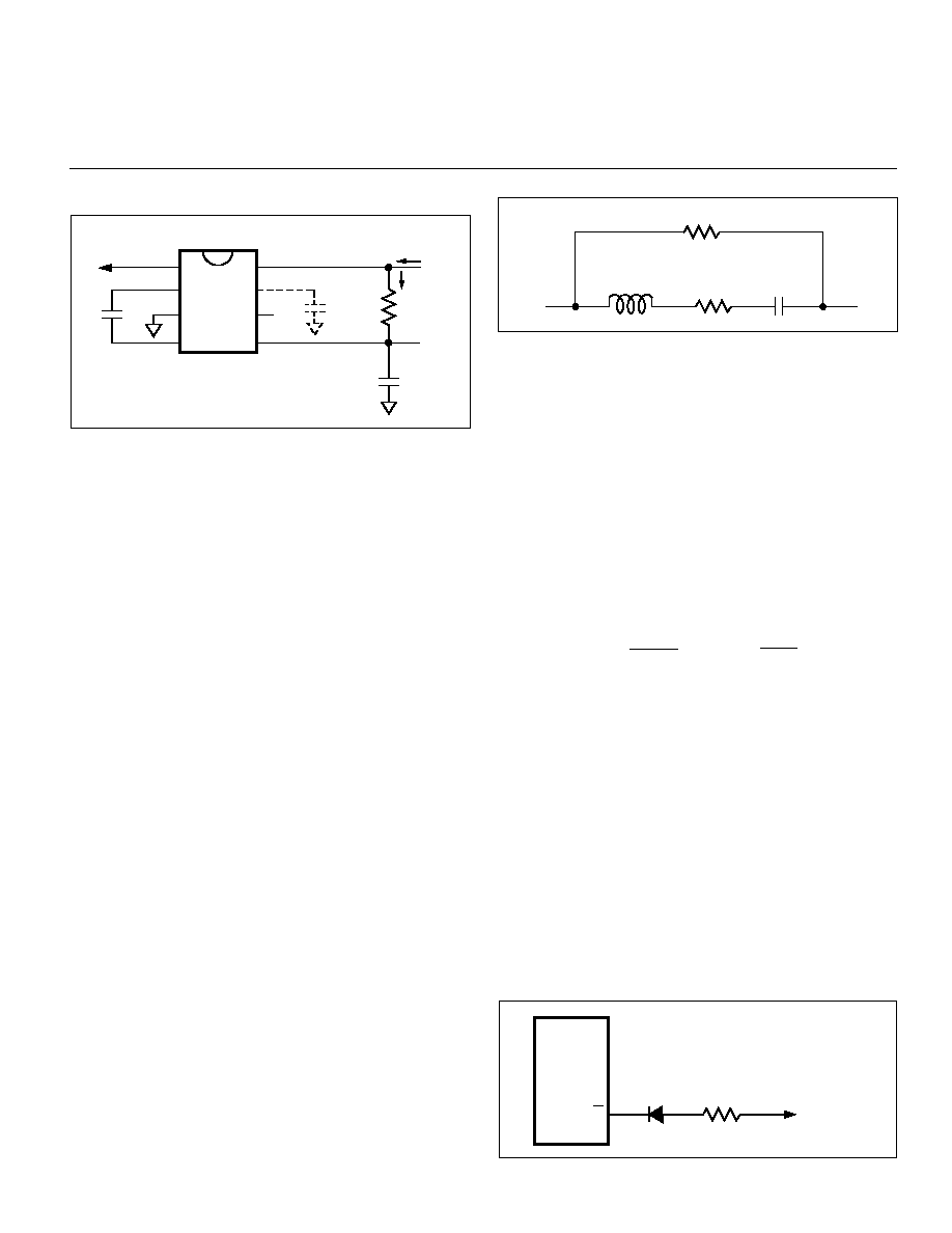
Synchronizing
The TC7662A may be synchronized by connecting pin
7 of the TC7662A through a 100k resistor in series with a
diode to a negative-going pulse source. The negative pulse
voltage can be +5V with a 5 microsecond duration going
negative to 0V.
TEST CIRCUIT
Figure 2. Synchronization
X
C
=
and Z
C
= ,
X
C
DS
APPLICATIONS INFORMATION
Theory of Operation
The TC7662A is a capacitive charge pump (some-
times called a switched-capacitor circuit), where four
MOSFET switches control the charge and discharge of a
capacitor.
The functional diagram (page 1) shows how the switch-
ing action works. SW1 and SW2 are turned on simulta-
neously, charging C1 to the supply voltage, V
DD
. This
assumes that the ON resistance of the MOSFETs in series
with the capacitor produce a charging time (3 time con-
stants) less than the ON time provided by the oscillator
frequency, as shown:
3 (R
DS(ON)
C1) <C1/(0.5 f
OSC
).
In the next cycle, SW1 and SW2 are turned OFF and,
after a very short interval with all switches OFF (preventing
large currents from occurring due to cross conduction),
SW3 and SW4 are turned ON. The charge in C1 is then
transferred to C
OUT
, BUT WITH THE POLARITY IN-
VERTED. In this way, a negative voltage is derived.
An oscillator supplies pulses to a flip-flop that is fed to a
set of level shifters. These level shifters then drive each set
of switches at one-half the oscillator frequency.
The oscillator has a pin that controls the frequency of
oscillation. Pin 7 can have a capacitor added that is con-
nected to ground. This will lower the frequency of the
oscillator by adding capacitance to the internal timing ca-
pacitor of the TC7662A. (See Oscillator Frequency vs. C
EXT
,
page 5.)
Capacitors
In early charge pump converters, capacitors were not
considered critical due to the high R
DS(ON)
of the MOSFET
switches. In order to understand this, let's look at a model of
a typical electrolytic capacitor (Figure 1).
1
2
f C
TC7662A
1
2
3
4
8
7
5
CP
+
10
µ
F
COSC
R L
V
(5V)
OUT
10
µ
F
C R
I L
IS
V
(+5V)
+
NC
NC
6
+
TTL
Q
Q
100 k
TO PIN 7
TC7662A
Figure 1. Capacitor Equivalent Circuit
EPR
ESL
ESR
C