 | ÐлекÑÑоннÑй компоненÑ: TC820CPL | СкаÑаÑÑ:  PDF PDF  ZIP ZIP |
Äîêóìåíòàöèÿ è îïèñàíèÿ www.docs.chipfind.ru
©
2002 Microchip Technology Inc.
DS21476B-page 1
TC820
Features
· Multiple Analog Measurement System
- Digit A/D Converter
- Frequency Counter
- Logic Probe
· Low Noise A/D Converter:
-
Differential Inputs: (1pA Bias Current)
-
On-Chip 50ppm/°C Voltage Reference
· Frequency Counter:
-
4MHz Maximum Input Frequency
-
Auto-Ranging Over Four Decade Range
· Logic Probe:
-
Two LCD Annunciators
-
Buzzer Driver
· 3-3/4 Digit Display with Over Range Indicator
· LCD Display Driver with Built-in Contrast Control
· Data Hold Input for Comparison Measurements
· Low Battery Detect with LCD Annunciator
· Under Range and Over Range Outputs
· On-Chip Buzzer Driver with Control Input
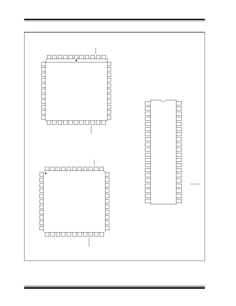
· 40-Pin Plastic DIP, 44-Pin Plastic Flat Pack, or
44-Pin PLCC Packages
Device Selection Table
General Description
The TC820 is a 3-3/4 digit, multi-measurement system
especially suited for use in portable instruments. It inte-
grates a dual slope A/D converter, auto-ranging fre-
quency counter and logic probe into a single 44-pin
surface mount, or 40-pin through hole package. The
TC820 operates from a single 9V input voltage (bat-
tery) and features a built-in battery low flag. Function
and decimal point selection are accomplished with sim-
ple logic inputs designed for direct connection to an
external microcontroller or rotary switch.
Part
Number
Resolution
Package
Operating
Temp. Range
TC820CPL
3-3/4 Digits
40-Pin PDIP
0
°
C to +70
°
C
TC820CKW
3-3/4 Digits
44-Pin PQFP
0
°
C to +70
°
C
TC820CLW
3-3/4 Digits
44-Pin PLCC
0
°
C to +70
°
C
3-3/4 Digit A/D Converter with Frequency Counter
and Logic Probe
TC820
DS21476B-page 2
©
2002 Microchip Technology Inc.
Package Type
TC820CPL
1
2
3
4
OSC1
5
6
7
8
9
10
11
12
13
14
15
16
17
18
19
20
40
39
38
37
36
35
34
33
32
31
30
29
28
27
26
25
24
23
22
21
OSC2
OSC3
C
REF
+
COM
V
SS
PKHOLD
FREQ/VOLTS
BUZIN
BUZOUT
DP1/HI
DP0/LO
27
28
29
30
31
32
33
7
4
3
2
1
C
AZ
12
13
14
15
17
18
44
43
42
41
39
38
40
AGD3
16
37
36
35
34
V
INT
19
20
21
22
26
8
25
9
24
10
23
11
5
6
BC3P2
DGND
33
34
35
36
37
38
39
13
10
9
8
7
C
AZ
18
19
20
21
23
24
UR
6
5
4
3
1
44
2
AGD3
AGD4
OSC3
22
43
OSC2
42
OSC1
41
EOC/HOLD
40
V
INT
25
26
27
28
32
14
31
15
30
16
29
17
V
DISP
HFE3
BC4P3
11
12
TC820CLW
V
BUFF
TC820CKW
44-Pin PQFP
44-Pin PLCC
40-Pin PDIP
C
REF
-
V
REF
+
V
REF
-
V
IN
-
V
IN
+
V
BUFF
C
AZ
V
INT
V
DD
RANGE/FREQ
LOGIC
ANNUNC
DGND
BP1
BP2
BP3
Segments BC1BT
Segments AGD1
Segments PKFE1
Segments BC2P1
Segments AGD2
Segments OFE2
Segments BC3P2
Segments AGD3
Segments HFE3
Segments BC4P3
Segments AGD4
Segments L-E4
L-E4
V
DD
V
IN
+
V
IN
-
V
REF
-
V
REF
+
C
REF
-
C
REF
+
COM
V
SS
OR
PKHOLD
FREQ/VOLTS
BUZIN
BUZOUT
DP1/HI
DP0/LO
RANGE/FREQ
LOGIC
ANNUNC
DGND
BP1
BP2
BP3
BP1BT
BC3P2
OFE2
AGD2
BC2P1
PKFE1
AGD1
LE4
UR
PKHOLD
AGD2
OFE2
V
DISP
BC2P1
PKFE1
BP2
OSC1
V
SS
OR
COM
C
REF
+
BC4P3
OSC3
OSC2
EOC/HOLD
ANNUNC
FREQ/VOLTS
BUZIN
BUZOUT
DP1/HI
DP0/LO
RANGE/FREQ
LOGIC
BP1
BP3
BC1BT
AGD1
V
BUFF
V
IN
+
V
IN
-
V
REF
-
V
REF
+
C
REF
-
HFE3
AGD4
V
DD
©
2002 Microchip Technology Inc.
DS21476B-page 3
TC820
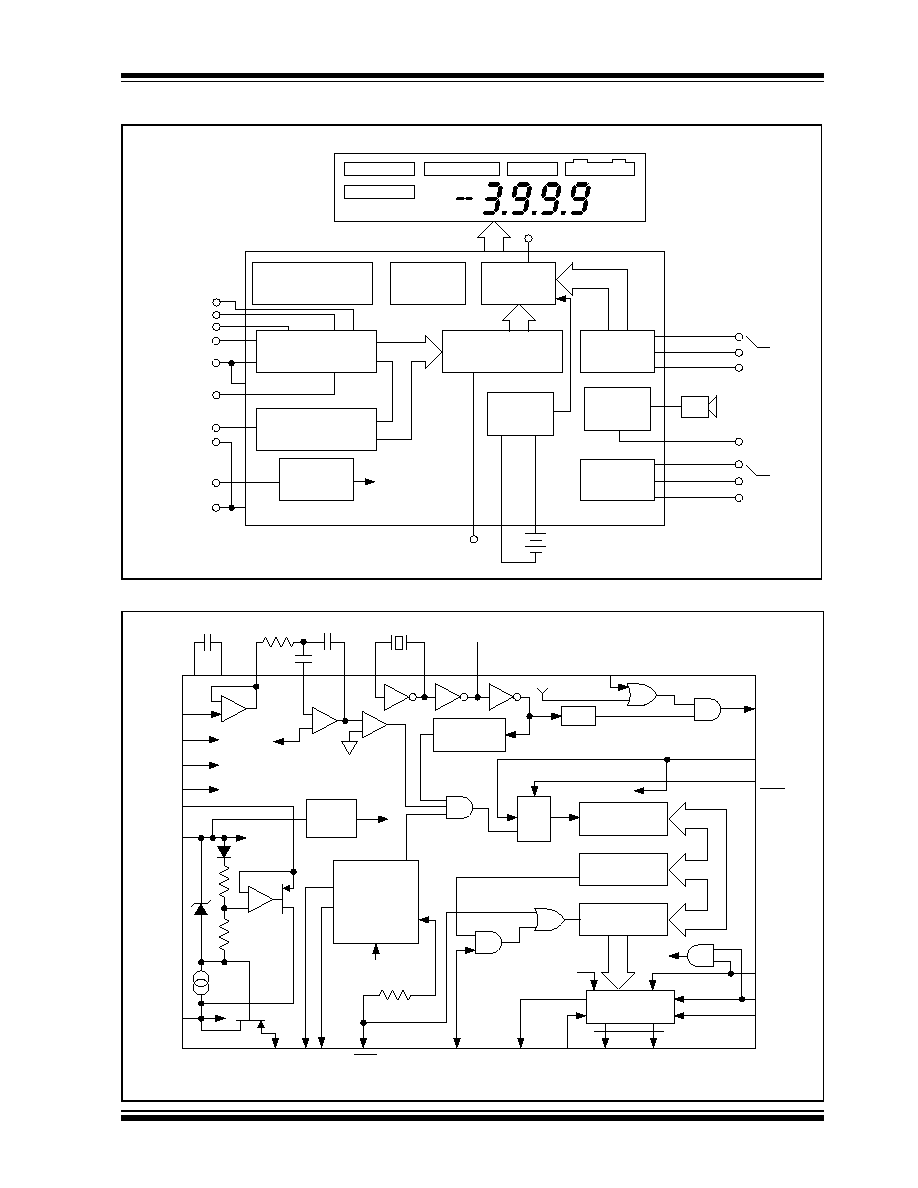
Typical Applications
Peak Hold
Comparator
3-3/4 Digit A/D
Converter
Low
Battery
Detect
Decimal
Point
Drivers
Buzzer
Driver
Function
Select
Logic Probe
Auto-Ranging
Frequency
Counter
Clock
Oscillator
Triple LCD
Drivers
Low Drift Voltage
Differential
Reference
Logic High
Logic Low
Over Range
PKHold
Low Batt
Annunciator Drive
Decimal
Point
Select
Buzzer
Control
Function
Select
Digital Ground
To LCD
and Buzzer
Peak
Hold
Logic Probe
Input
Frequency Input
Full Scale Select
Under Range
Over Range
Analog GND
Volts
Frequency
Logic
Triplex LCD
9V
TC820
Analog Input
+
EOC
Range Frequency
Input
Triples
Drivers
Display
Latch
Comparator
A > B
A/D Counter
(3999 Counts)
Logic
Low
Logic
DP0/LO
DP1/HI
Range/
Frequency
Frequency/
Volts
Buzzer
Driver
BUZIN
Logic
Low
OSC3
OSC2
OSC1
Frequency Counter Input
A/D Counter Select
Range
SEL
B
A
Low Batt
Low
Batt
Detect
A/D Control
DEINT
Under Range
Over Range
Range
EOC
DGND UR OR
EOC/
HOLD
PEAK
HOLD
ANNUNC
SEG0 · · · BP3
V
DISP
15
To LCD
V
INT
C
AZ
Common
V
DD
V
SS
V
REF
+
V
REF
-
TC820
V
IN
+
V
IN
-
C
REF
+
C
REF
- V
BUFF
÷2
÷8
TC820
DS21476B-page 4
©
2002 Microchip Technology Inc.
1.0
ELECTRICAL
CHARACTERISTICS
Absolute Maximum Ratings*
Supply Voltage (V
DD
to GND) ................................ 15V
Analog Input Voltage:
(Either Input) (Note 1) ............................ V
DD
to V
SS
Reference Input Voltage (Either Input) ....... V
DD
to V
SS
Digital Inputs........................................... V
DD
to DGND
V
DISP
....................................... V
DD
to (DGND 0.3V)
Package Power Dissipation (T
A
70°C) (Note 2):
40-Pin Plastic DIP ......................................... 1.23W
44-Pin PLCC ..................................................1.23W
44-Pin Plastic Flat Package (PQFP) ..............1.00W
Operating Temperature Range:
"C" Devices ......................................... 0°C to +70°C
"E" Devices.......................................-40°C to +85°C
Storage Temperature Range .............. -65°C to +150°C
*Stresses above those listed under "Absolute Maximum
Ratings" may cause permanent damage to the device. These
are stress ratings only and functional operation of the device
at these or any other conditions above those indicated in the
operation sections of the specifications is not implied.
Exposure to Absolute Maximum Rating conditions for
extended periods may affect device reliability.
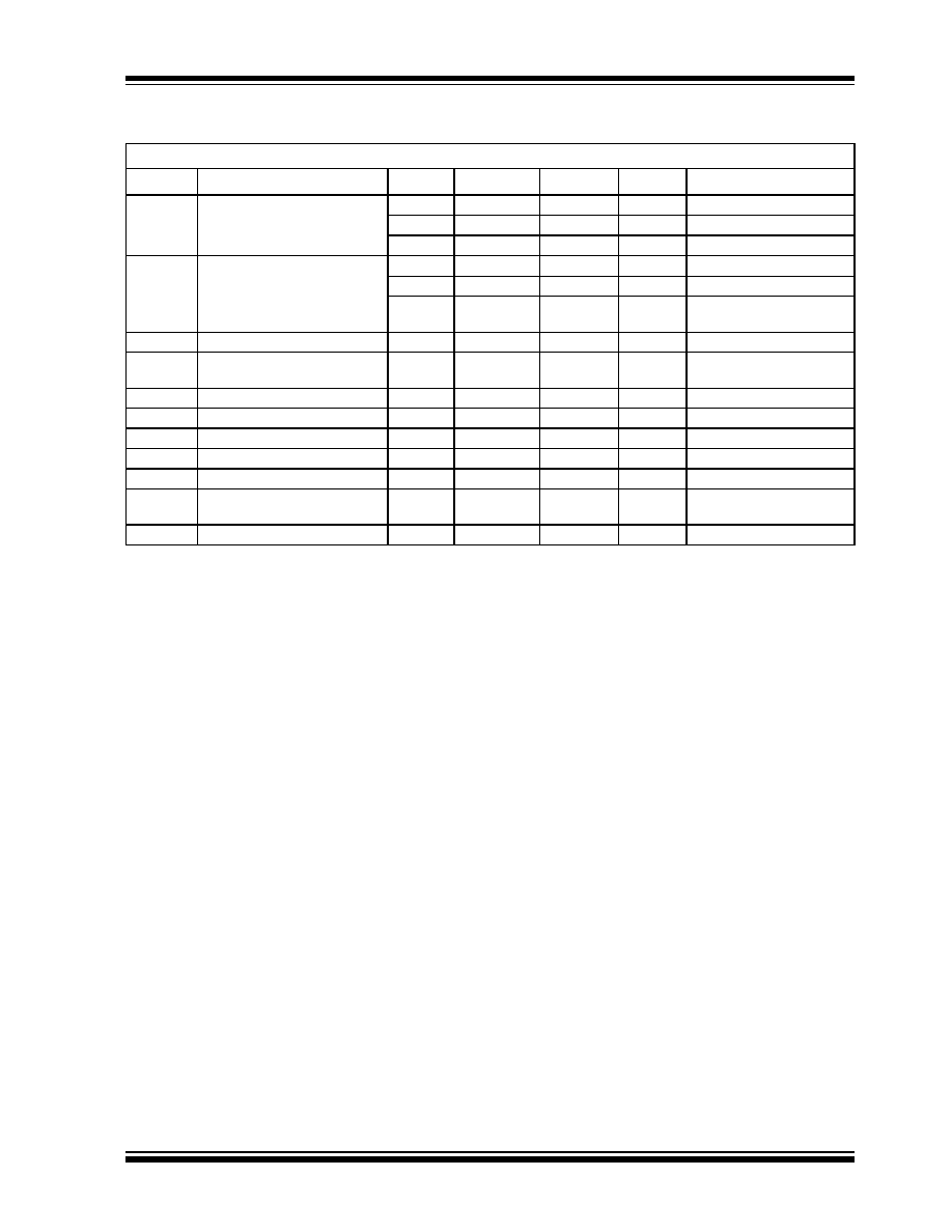
TC820 ELECTRICAL SPECIFICATIONS
Electrical Characteristics:
V
S
= 9V, T
A
= 25°C, unless otherwise specified.
Symbol
Parameter
Min
Typ
Max
Units
Test Conditions
Zero Input Reading
-000
±000
+000
Digital
Reading
V
IN
= 0V
Full Scale = 400mV
RE
Rollover Error
-1
±0.2
+1
Counts
V
IN
= ±390mV
Full Scale = 400mV
NL
Nonlinearity
(Maximum Deviation From Best
Straight Line Fit)
-1
±0.2
+1
Count
Full Scale = 400mV
Ratiometric Reading
1999
1999/2000
2000
--
V
IN
= V
REF
, TC820
CMRR
Common Mode Rejection Ratio
--
50
--
µ
V/V
V
CM
= ±1V, V
IN
= 0V
Full Scale = 400mV
(V
FS
= 200mV)
VCMR
Common Mode Voltage Range
V
SS
+ 1.5
--
V
DD
1
Input High, Input Low
e
N
Noise (P-P Value Not
Exceeded 95% of Time)
--
15
--
µ
V
V
IN
= 0V
Full Scale = 400mV
I
IN
Input Leakage Current
--
--
--
--
V
IN
= 0V
--
1
10
pA
T
A
= 25°C
--
20
--
pA
0°C
T
A
+70°C
--
100
--
pA
-40°C
T
A
+85°C
V
COM
Analog Common Voltage
3.15
3.3
3.45
V
25k
between Common and
V
DD
(V
SS
- V
COM
)
V
CTC
Common Voltage Temperature
Coefficient
--
--
--
--
25k
Between Common and
V
DD
--
35
50
ppm/°C
0°C
T
A
+70°C
--
50
--
--
-40°C
T
A
+85°C
Note
1:
Input voltages may exceed the supply voltages provided that input current is limited to ±100
µ
A. Current above this value
may result in invalid display readings, but will not destroy the device if limited to ±1mA.
2:
Dissipation ratings assume device is mounted with all leads soldered to printed circuit board.
©
2002 Microchip Technology Inc.
DS21476B-page 5
TC820
TC
ZS
Zero Reading Drift
--
--
--
--
V
IN
= 0V
--
0.2
--
--
0°C
T
A
+70°C
--
1
--
--
-40°C
T
A
+85°C
TC
FS
Scale Factor Temperature
Coefficient
--
--
--
--
V
IN
= 399mV
--
1
5
ppm/°C
0°C
T
A
+70°C
--
5
--
ppm/°C
-40°C
T
A
+85°C
Ext Ref = 0ppm/°C
I
S
Supply Current
--
1
1.5
mA
V
IN
= 0V
Peak-to-Peak Backplane
Drive Voltage
4.25
4.7
5.3
V
V
S
= 9V
V
DISP
= DGND
Buzzer Frequency
--
5
--
kHz
F
OSC
= 40kHz
Counter TIme-Base Period
--
1
--
Second
F
OSC
= 40kHz
Low Battery Flag Voltage
6.7
7
7.3
V
V
DD
to V
SS
V
IL
Input Low Voltage
--
--
DGND + 1.5
V
V
IH
Input High Voltage
V
DD
1.5
--
--
V
V
OL
Output Low Voltage,
UR, OR Outputs
V
DD
1.5
--
DGND + 0.4
V
I
L
= 50
µ
A
Control Pin Pull-down Current
--
5
--
µ
A
V
IN
= V
DD
TC820 ELECTRICAL SPECIFICATIONS (CONTINUED)
Electrical Characteristics:
V
S
= 9V, T
A
= 25°C, unless otherwise specified.
Symbol
Parameter
Min
Typ
Max
Units
Test Conditions
Note
1:
Input voltages may exceed the supply voltages provided that input current is limited to ±100
µ
A. Current above this value
may result in invalid display readings, but will not destroy the device if limited to ±1mA.
2:
Dissipation ratings assume device is mounted with all leads soldered to printed circuit board.