 | ÐлекÑÑоннÑй компоненÑ: TC826CBU | СкаÑаÑÑ:  PDF PDF  ZIP ZIP |
Äîêóìåíòàöèÿ è îïèñàíèÿ www.docs.chipfind.ru
©
2002 Microchip Technology Inc.
DS21477B-page 1
TC826
Features
· Bipolar A/D Conversion
· 2.5% Resolution
· Direct LCD Display Drive
· `Thermometer' BAR or DOT Display
· 40 Data Segments Plus Zero
· Over Range Plus Polarity Indication
· Precision On-Chip Reference: 35ppm/°C
· Differential Analog Input
· Low Input Leakage: 10pA
· Display Flashes on Over Range
· Display HOLD Mode
· Auto-Zero Cycle Eliminates Zero Adjust
Potentiometer
· 9V Battery Operation
· Low Power Consumption: 1.1mW
· 20mV to 2.0V Full Scale Operation
· Non-Multiplexed LCD Drive for Maximum
Viewing Angle
Device Selection Table
General Description
In many applications, a graphical display is preferred
over a digital display. Knowing a process or system
operates, for example, within design limits is more valu-
able than a direct system variable read out. A bar or
moving dot display supplies information precisely with-
out requiring further interpretation by the viewer.
The TC826 is a complete analog-to-digital converter
with direct liquid crystal (LCD) display drive. The 40
LCD data segments plus zero driver give a 2.5% reso-
lution bar display. Full scale differential input voltage
range extends from 20mV to 2V. The TC826 sensitivity
is 500
µ
V. A low drift 35ppm/°C internal reference, LCD
backplane oscillator and driver, input polarity LCD
driver, and over range LCD driver make designs simple
and low cost. The CMOS design required only 125µA
from a 9V battery. In +5V systems, a TC7660 DC to DC
converter can supply the -5V supply. The differential
analog input leakage is a low 10pA.
Two display formats are possible. The BAR mode dis-
play is like a `thermometer' scale. The LCD segment
driver that equals the input, plus all below it are on. The
DOT mode activates only the segment equal to the
input. In either mode, the polarity signal is active for
negative input signals. An over range input signal
causes the display to flash and activates the over range
annunciator. A HOLD mode can be selected that
freezes the display and prevents updating.
The dual slope integrating conversion method with
auto-zero phase maximizes noise immunity and elimi-
nates zero scale adjustment
potentiometers. Zero
scale drift is a low 5
µ
V/°C. Conversion rate is typically
5 per second and is adjustable by a single external
resistor.
A compact, 0.5" square, flat package minimizes PC
board area. The high pin count LSI package makes
multiplexed LCD displays unnecessary. Low cost,
direct drive LCD displays offer the widest viewing angle
and are readily available. A standard display is avail-
able now for TC826 prototyping work.
Part Number
Package
Temperature Range
TC826CBU
64-Pin PQFP
0
°
C to +70
°
C
Analog-to-Digital Converter with Bar Graph Display Output
TC826
DS21477B-page 2
©
2002 Microchip Technology Inc.
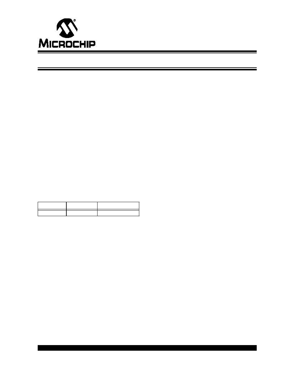
Package Type
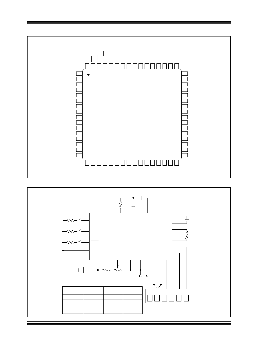
Typical Application
30
29
28
50
51
25
52
24
53
23
54
22
55
21
56
20
57
19
58
18
59
17
60
31
BAR 35
BAR 36
BAR 37
BAR 38
BAR 39
BAR 40
OR
POL-
BAR/DOT
HOLD
TEST
5
6
7
8
9
10
11
12
13
14
15
41
40
39
38
37
36
35
34
33
47
46
62
63
64
49
26
BAR 15
NC
BAR 34
1
2
3
4
45
44
43
42
BAR 30
BAR 14
BAR 13
BAR 12
BAR 11
BAR 10
BAR 9
BAR 8
BAR 7
BAR 6
BAR 5
BAR 4
BAR 3
BAR 2
BAR 1
BAR 29
BAR 28
BAR 27
BAR 26
BAR 25
BAR 24
BAR 23
BAR 22
BAR 21
BAR 20
BAR 19
BAR 18
NC
16
48
32
61
OSC1
BP
ANALOG
COMMON
+IN
-IN
REF IN
V
DD
V
SS
OSC2
BAR 0
C
REF
+
C
REF
-
V
BUF
C
AZ
V
INT
NC
NC
BAR 17
BAR 16
BAR 32
BAR 33
BAR 31
TC826CBU
27
64-Pin PQFP
5
8
2
4
3
60
Segment Drive
59
15
TC826
C
INT
C
AZ
R
INT
R
2
R
1
-IN +IN
9V
12
63
62
61
14
7
6
13
C
REF
1.0mf
R
OSC
430k
Backplane
41 Segment LCD
Bar Graph
11
10
9
V
BUF
C
AZ
V
INT
C
REF
+
C
REF
-
OSC1
OSC2
BP
OR
BAR/DOT
HOLD
TEST
V
SS
V
DD
REF
IN
ANALOG
COMMON -IN +IN
BAR 0-
BAR 40 POL-
OR
1M
1M
1M
Component
2V
Full Scale
200mV
Full Scale
20mV
Full Scale
R
INT
C
INT
C
REF
2M
20k
20k
0.033mf
0.033mf
0.033mf
1mf
1mf
1mf
C
AZ
0.068mf
0.068mf
0.014mf
R
1
+ R
2
= 250k
©
2002 Microchip Technology Inc.
DS21477B-page 3
TC826
1.0
ELECTRICAL
CHARACTERISTICS
Absolute Maximum Ratings*
Supply Voltage (V+ to V-) ....................................... 15V
Analog Input Voltage (Either Input) (Note 1)... V+ to V-
Power Dissipation (T
A
70°C)
64-Pin Plastic Flat Package ............................... 1.14W
Operating Temperature Range:
Commercial Package (C) ........................ 0°C to +70°C
Storage Temperature Range .............. -65°C to +150°C
*Stresses above those listed under "Absolute Maximum
Ratings" may cause permanent damage to the device. These
are stress ratings only and functional operation of the device
at these or any other conditions above those indicated in the
operation sections of the specifications is not implied.
Exposure to Absolute Maximum Rating conditions for
extended periods may affect device reliability.
TC826 ELECTRICAL SPECIFICATIONS
Note
1: Input voltages may exceed the supply voltages when the input current is limited to 100
µ
A.
2: Static sensitive device. Unused devices should be stored in conductive material to protect devices from static discharge
and static fields.
3: Backplane drive is in phase with segment drive for `off' segment and 180°C out of phase for `on' segment. Frequency is
10 times conversion rate.
4: Logic input pins 58, 59, and 60 should be connected through 1M
series resistors to V
SS
for logic 0.
Electrical Characteristics: V
S
= 9V; R
OSC
= 430k
; T
A
= 25°C; Full Scale = 20mV, unless otherwise stated.
Symbol
Parameter
Min
Typ
Max
Unit
Test Conditions
Zero Input
-0
±0
+0
Display
V
IN
= 0.0V
Zero Reading Drift
--
0.2
1
µ
V/°C
V
IN
= 0.0V
0°C
T
A
+70°C
NL
Linearity Error
-1
0.5
+1
Count
Max Deviation from Best Straight Line
R/O
Rollover Error
-1
0
+1
Count
-V
IN
= +V
IN
EN
Noise
--
60
--
µ
V
P-P
V
IN
= 0V
ILK
Input Leakage Current
--
10
20
pA
V
IN
= 0V
CMRR
Common Mode Rejection Ratio
--
50
--
µ
V/V
VCM = ±1V
V
IN
= 0V
Scale Factor Temperature Coefficient
--
1
--
ppm/°C
0
T
A
7 +0°C
External Ref. Temperature
Coefficient = 0ppm/°C
V
CTC
Analog Common Temperature
Coefficient
--
35
100
ppm/°C
250k
between Common and
V+, 0°C
T
A
+70°C
V
COM
Analog Common Voltage
2.7
2.9
3.35
V
250k
between Common and V
DD
VSD
LCD Segment Drive Voltage
4
5
6
V
P-P
VBD
LCD Backplane Drive Voltage
4
5
6
V
P-P
I
DD
Power Supply Current
--
125
175
µ
A
TC826
DS21477B-page 4
©
2002 Microchip Technology Inc.
2.0
PIN DESCRIPTION
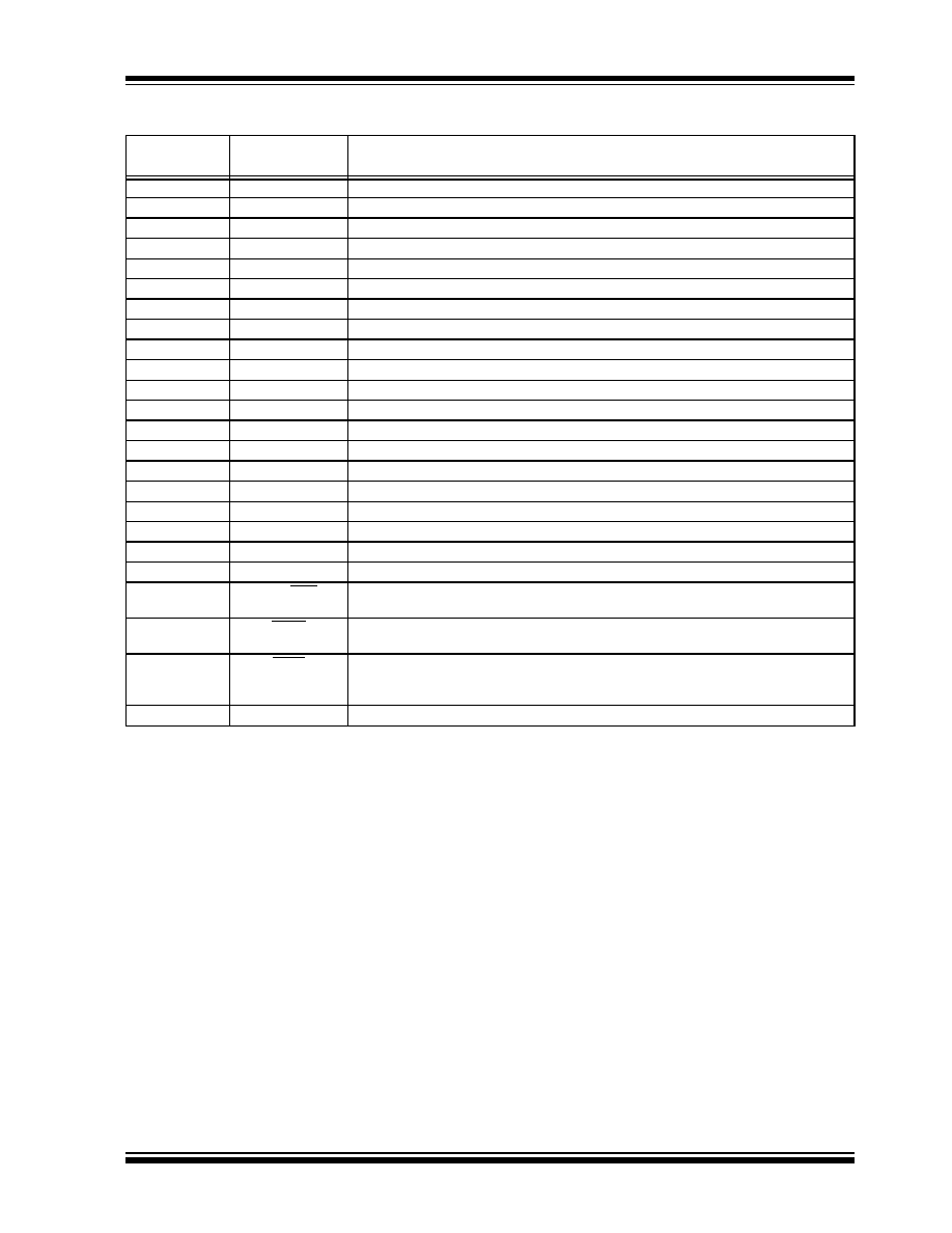
The descriptions of the pins are listed in Table 2-1.
TABLE 2-1:
PIN FUNCTION TABLE
Pin Number
(64-Pin PQFP)
Symbol
Description
1
NC
Positive analog signal input.
2
ANALOG
COMMON
Establishes the internal analog ground point. Analog common is set to 2.9V below the
positive supply COMMON by an internal zener reference circuit. The voltage difference
between V
DD
and analog common can be used to supply the TC826 voltage reference
input at REF IN (Pin 5).
3
+IN
Positive analog signal input.
4
-IN
Negative analog signal input.
5
REF IN
Reference voltage positive input. Measured relative to analog common.
REF IN
Full Scale/2.
6
C
REF
+
Reference capacitor connection.
7
C
REF
-
Reference capacitor connection.
8
V
DD
Positive supply terminal.
9
V
BUF
Buffer output. Integration resistor connection.
10
C
AZ
Negative comparator input. Auto-zero capacitor connection.
11
V
INT
Integrator output. Integration capacitor connection.
12
V
SS
Negative supply terminal.
13
OSC1
Oscillator resistor (R
OSC
) connection.
14
OSC2
Oscillator resistor (R
OSC
) connection.
15
BP
LCD Backplane driver.
16
BAR 0
LCD Segment driver: Bar 0.
17
NC
No connection.
18
BAR 1
LCD Segment driver: Bar 1.
19
BAR 2
LCD Segment driver: Bar 2.
20
BAR 3
LCD Segment driver: Bar 3.
21
BAR 4
LCD Segment driver: Bar 4.
22
BAR 5
LCD Segment driver: Bar 5.
23
BAR 6
LCD Segment driver: Bar 6.
24
BAR 7
LCD Segment driver: Bar 7.
25
BAR 8
LCD Segment driver: Bar 8.
26
BAR 9
LCD Segment driver: Bar 9.
27
BAR 10
LCD Segment driver: Bar 10.
28
BAR 11
LCD Segment driver: Bar 11.
29
BAR 12
LCD Segment driver: Bar 12.
30
BAR 13
LCD Segment driver: Bar 13.
31
BAR 14
LCD Segment driver: Bar 14.
32
BAR 15
LCD Segment driver: Bar 15.
33
BAR 16
LCD Segment driver: Bar 16.
34
BAR 17
LCD Segment driver: Bar 17.
35
BAR 18
LCD Segment driver: Bar 18.
36
BAR 19
LCD Segment driver: Bar 19.
37
BAR 20
LCD Segment driver: Bar 20.
38
BAR 21
LCD Segment driver: Bar 21.
39
BAR 22
LCD Segment driver: Bar 22.
40
BAR 23
LCD Segment driver: Bar 23.
©
2002 Microchip Technology Inc.
DS21477B-page 5
TC826
41
BAR 24
LCD Segment driver: Bar 24.
42
BAR 25
LCD Segment driver: Bar 25.
43
BAR 26
LCD Segment driver: Bar 26.
44
BAR 27
LCD Segment driver: Bar 27.
45
BAR 28
LCD Segment driver: Bar 28.
46
BAR 29
LCD Segment driver: Bar 29.
47
BAR 30
LCD Segment driver: Bar 30.
48
NC
No connection.
49
BAR 31
LCD Segment driver: Bar 31.
50
BAR 32
LCD Segment driver: Bar 32.
51
BAR 33
LCD Segment driver: Bar 33.
52
BAR 34
LCD Segment driver: Bar 34.
53
BAR 35
LCD Segment driver: Bar 35.
54
BAR 36
LCD Segment driver: Bar 36.
55
BAR 37
LCD Segment driver: Bar 37.
56
BAR 38
LCD Segment driver: Bar 38.
57
BAR 39
LCD Segment driver: Bar 39.
58
BAR 40
LCD Segment driver: Bar 40.
59
OR
LCD segment driver that indicated input out-of-range condition.
60
POL-
LCD segment driver that indicates input signal is negative.
61
BAR/DOT
Input logic signal that selects BAR or DOT display format. Normally in BAR mode. Connect
to V
SS
through 1M
resistor for DOT format.
62
HOLD
Input logic signal that prevents display from changing. Pulled high internally to inactive
state. Connect to V
SS
through 1M
series resistor for HOLD mode operation.
63
TEST
Input logic signal. Sets TC826 to BAR Display mode. BAR 0 to 40, plus OR flash on and
off. The POL- LCD driver is on. Pulled high internally to inactive state. Connect to V
SS
with
1M
series resistor to activate.
64
NC
No connection.
TABLE 2-1:
PIN FUNCTION TABLE (CONTINUED)
Pin Number
(64-Pin PQFP)
Symbol
Description