PRODUCTS AND SPECIFICATIONS DISCUSSED HEREIN ARE SUBJECT TO CHANGE BY MICRON WITHOUT NOTICE.
09005aef80a3e0d6
DDA16C32_64_128x64AG_C.fm - Rev. C 8/03 EN
1
©2003 Micron Technology, Inc.
256MB, 512MB, 1GB (x64), PC3200
184-PIN UNBUFFERED DDR SDRAM DIMM
DDR SDRAM
DIMM
MT16VDDT3264A ≠ 256MB
MT16VDDT6464A ≠ 512MB
MT16VDDT12864A ≠ 1GB
For the latest data sheet, please refer to the Micron
‚
Web
site:
www.micron.com/moduleds
Features
∑ 184-pin, dual in-line memory module (DIMM)
∑ Fast data transfer rates: PC3200
∑ CAS Latency 3
∑ Utilizes 400 MT/s DDR SDRAM components
∑ 256MB (32 Meg x 64), 512MB (64 Meg x 64), and 1GB
(128 Meg x 64)
∑ V
DD
= V
DD
Q = +2.6V
∑ V
DDSPD
= +2.3V to +3.6V
∑ 2.6V I/O (SSTL_2 compatible)
∑ Commands entered on each positive CK edge
∑ DQS edge-aligned with data for READs; center-
aligned with data for WRITEs
∑ Internal, pipelined double data rate (DDR)
architecture; two data accesses per clock cycle
∑ Bidirectional data strobe (DQS) transmitted/
received with data--i.e., source-synchronous data
capture
∑ Differential clock inputs CK and CK#
∑ Four internal device banks for concurrent operation
∑ Programmable burst lengths: 2, 4, or 8
∑ Auto precharge option
∑ Auto Refresh and Self Refresh Modes
∑ 15.6µs (256MB), 7.8125µs (512MB and 1GB)
maximum average periodic refresh interval
∑ Serial Presence Detect (SPD) with EEPROM
∑ Programmable READ CAS latency
∑ Gold edge contacts
Figure 1: 184-Pin DIMM (MO-206)
OPTIONS
MARKING
∑ Package
184-pin DIMM (Standard)
G
184-pin DIMM (Lead-free)
Y
∑ Memory Clock/Speed, CAS Latency
5ns (200MHz), 400 MT/s, CL = 3
-40B
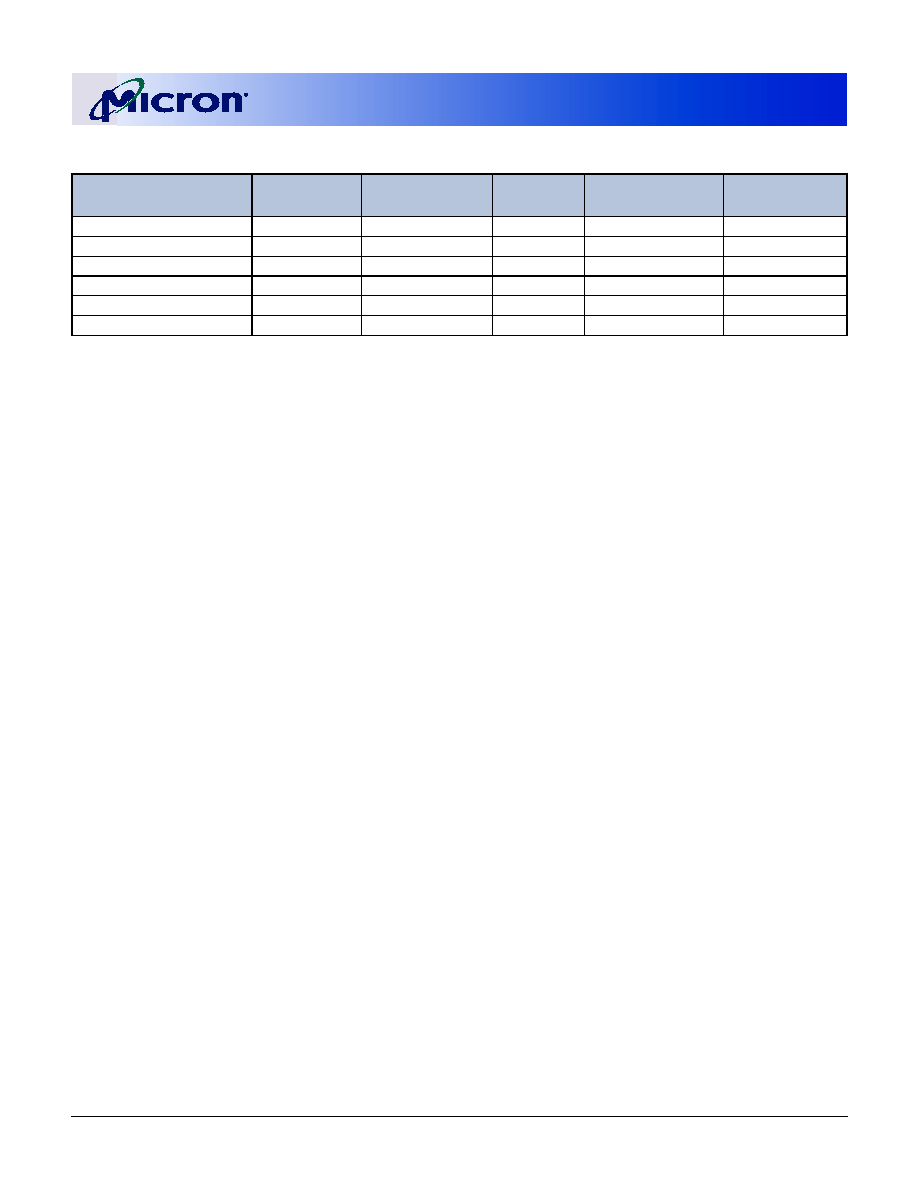
Table 1:
Address Table
256MB
512MB
1GB
Refresh Count
4K
8K
8K
Row Addressing
4K (A0≠A11)
8K (A0≠A12)
8K (A0≠A12)
Device Bank Addressing
4 (BA0, BA1)
4 (BA0, BA1)
4 (BA0, BA1)
Device Configuration
16 Meg x 8
32 Meg x 8
64 Meg x 8
Column Addressing
1K (A0≠A9)
1K (A0≠A9)
2K (A0≠A9, A11)
Module Rank Addressing
2 (S0#, S1#)
2 (S0#, S1#)
2 (S0#, S1#)

256MB, 512MB, 1GB (x64), PC3200
184-PIN UNBUFFERED DDR SDRAM DIMM
09005aef80a3e0d6
Micron Technology, Inc., reserves the right to change products or specifications without notice.
DDA16C32_64_128x64AG_C.fm - Rev. C 8/03 EN
4
©2003 Micron Technology, Inc.
Table 5:
Pin Descriptions
Pin numbers may not correlate with symbols. Refer to Pin Assignment Tables on page 3 for more information
PIN NUMBERS
SYMBOL
TYPE
DESCRIPTION
1
V
REF
Input
SSTL_2 reference voltage.
63, 65, 154
WE#, CAS#, RAS#
Input
Command Inputs: RAS#, CAS#, and WE# (along with S#) define
the command being entered.
16, 17, 75, 76, 137, 138
CK0, CK0#, CK1,
CK1#, CK2, CK2#
Input
Clock: CK, CK# are differential clock inputs. All address and
control input signals are sampled on the crossing of the
positive edge of CK,and negative edge of CK#. Output data
(DQs and DQS) is referenced to the crossings of CK and CK#.
21, 111
CKE0, CKE1
Input
Clock Enable: CKE HIGH activates and CKE LOW deactivates
the internal clock, input buffers and output drivers. Taking
CKE LOW provides PRECHARGE POWER-DOWN and SELF
REFRESH operations (all device banks idle), or ACTIVE POWER-
DOWN (row ACTIVE in any device bank). CKE is synchronous
for POWER-DOWN entry and exit, and for SELF REFRESH entry.
CKE is asynchronous for SELF REFRESH exit and for disabling
the outputs. CKE must be maintained HIGH throughout read
and write accesses. Input buffers (excluding CK, CK# and CKE)
are disabled during POWER-DOWN. Input buffers (excluding
CKE) are disabled during SELF REFRESH. CKE is an SSTL_2 input
but will detect an LVCMOS LOW level after V
DD
is applied and
until CKE is first brought to HIGH. After CKE has been brought
HIGH, it is an SSTL_2 input only.
157, 158
S0#, S1#
Input
Chip Selects: S# enables (registered LOW) and disables
(registered HIGH) the command decoder. All commands are
masked when S# is registered HIGH. S# is considered part of
the command code.
52, 59
BA0, BA1
Input
Bank Address: BA0 and BA1 define to which device bank an
ACTIVE, READ, WRITE, or PRECHARGE command is being
applied.
27, 29, 32, 37, 41, 43, 48, 115
(512MB, 1GB)
, 118, 122, 125,
130, 141
A0-A11
(256MB)
A0-A12
(512MB, 1GB)
Input
Address Inputs: Provide the row address for ACTIVE
commands, and the column address and auto precharge bit
(A10) for READ/WRITE commands, to select one location out
of the memory array in the respective device bank. A10
sampled during a PRECHARGE command determines whether
the PRECHARGE applies to one device bank (A10 LOW, device
bank selected by BA0, BA1) or all device banks (A10 HIGH).
The address inputs also provide the op-code during a MODE
REGISTER SET command. BA0 and BA1 define which mode
register (mode register or extended mode register) is loaded
during the LOAD MODE REGISTER command.
5, 14, 25, 36, 56, 67, 78, 86
DQS0-DQS7
Input/
Output
Data Strobe: Output with READ data, input with WRITE data.
DQS is edge-aligned with READ data, centered in WRITE data.
Used to capture data.
97, 107, 119, 129, 149, 159,
169, 177
DQS9/DM0
≠
DQS16/DM7
Input
Data Write Mask: DQS9-DQS16 function as DM0-DM7.
DM LOW allows WRITE operation. DM HIGH blocks WRITE
operation. DM lines do not affect READ operation.

256MB, 512MB, 1GB (x64), PC3200
184-PIN UNBUFFERED DDR SDRAM DIMM
09005aef80a3e0d6
Micron Technology, Inc., reserves the right to change products or specifications without notice.
DDA16C32_64_128x64AG_C.fm - Rev. C 8/03 EN
5
©2003 Micron Technology, Inc.
2, 4, 6, 8, 12, 13, 19, 20, 23,
24, 28, 31, 33, 35, 39, 40, 53,
55, 57, 60, 61, 64, 68, 69, 72,
73, 79, 80, 83, 84, 87, 88, 94,
95, 98, 99, 105, 106, 109,
110, 114, 117, 121, 123, 126,
127, 131, 133, 146, 147, 150,
151, 153, 155, 161, 162, 165,
166, 170, 171, 174, 175, 178,
179
DQ0-DQ63
Input/
Output
Data I/Os: Data bus.
92
SCL
Input
Serial Clock for Presence-Detect: SCL is used to synchronize the
presence-detect data transfer to and from the module.
181,182, 183
SA0-SA2
Input
Presence-Detect Address Inputs: These pins are used to
configure the presence-detect device.
91
SDA
Input/
Output
Serial Presence-Detect Data: SDA is a bidirectional pin used to
transfer addresses and data into and out of the presence-
detect portion of the module.
15, 22, 30, 54, 62, 77, 96,
104, 112, 128, 136, 143, 156,
164, 172, 180
V
DDQ
Supply
DQ Power Supply: +2.6V ±0.1V.
7, 38, 46, 70, 85, 108, 120,
148, 168
V
DD
Supply
Power Supply: +2.6V ±0.1V.
3, 11, 18, 26, 34, 42, 50, 58,
66, 74, 81, 89, 93, 100, 116,
124, 132, 139, 145, 152, 160,
176
V
SS
Supply
Ground.
184
V
DDSPD
Supply
Serial EEPROM positive power supply: +2.3V to +3.6V.
44, 45, 47, 49, 51, 134, 135,
140, 142, 144
DNU
--
Do Not Use: These pins are not connected on these modules,
but are assigned pins on other modules in this product family.
9, 10, 71, 82, 90, 101, 102,
103, 113, 115 (256MB), 163,
167, 173
NC
--
No Connect: These pins should be left unconnected.
Table 5:
Pin Descriptions (Continued)
Pin numbers may not correlate with symbols. Refer to Pin Assignment Tables on page 3 for more information
PIN NUMBERS
SYMBOL
TYPE
DESCRIPTION