Document Outline
- Features
- Options
- Key Timing Parameters
- Front View (128MB) 168-Pin DIMM
- Pin Assignment
- Part Numbers
- General Description
- EDO Page Mode
- Refresh
- Functional Block Diagrams
- Pin Descriptions
- Presence-Detect Truth Table
- Absolute Maximum Ratings
- DC Electrical Characteristics and Operating Conditions
- IDD Operating Conditions and Maximum Limits
- Capacitance
- EDO Page Mode - AC Electrical Characteristics
- Read Cycle
- Early Write Cycle
- EDO-Page-Mode Read Cycle
- EDO-Page-Mode Early Write Cycle
- Read-Write Cycle (LATE WRITE and READ-MODIFY-WRITE cycles)
- EDO-Page-Mode Read-Write Cycle (LATE WRITE and READ-MODIFY-WRITE cycle)
- EDO-Page-Mode Read Early Write Cycle (Pseudo READ-MODIFY-WRITE)
- EDO Read Cycle (with WE#-controlled disable)
- RAS#-Only Refresh Cycle
- CBR Refresh Cycle (Addresses, OE# = Don't Care)
- Hidden Refresh Cycle (WE# = Hight; OE# = LOW)
- 168-Pin DIMM (64MB SOJ)
- 168-Pin DIMM 64MB TSOP
- 168-Pin DIMM (128MB SOJ)
- 168-Pin DIMM (128MB TSOP)
- 168-Pin DIMM (128MB TSOP)
- 168-Pin DIMM (256MB SOJ)
- 168-Pin DIMM (256MB TSOP)
- 168-Pin DIMM (256MB SOJ)

1
8, 16, 32 Meg x 72 Buffered DRAM DIMMs
Micron Technology, Inc., reserves the right to change products or specifications without notice.
DM77_2.p65 ≠ Rev. 3/00
©2000, Micron Technology, Inc.
8, 16, 32 MEG x 72
BUFFERED DRAM DIMMs
FEATURES
∑ JEDEC-standard ECC pinout in a 168-pin, dual in-
line memory module (DIMM)
∑ 64MB (8 Meg x 72), 128MB (16 Meg x 72), and
256MB (32 Meg x 72)
∑ High-performance CMOS silicon-gate process
∑ Single +3.3V ±0.3V power supply
∑ All inputs, outputs, and clocks are LVTTL-compatible
∑ All inputs are buffered except RAS#
∑ 4,096-cycle CAS#-BEFORE-RAS# (CBR) refresh
distributed across 64ms
∑ Extended Data-Out (EDO) PAGE MODE access cycle
OPTIONS
MARKING
∑ Components
SOJ
D
TSOP
DT
∑ Package
168-pin DIMM (gold)
G
∑ Refresh Addressing
4,096 (4K) rows
Blank
8,192 (8K) rows
F
∑ Module Height
Low profile, 1.65" (256MB only)
C
Low profile, 1.25" (128MB only)
D
∑ Timing
50ns access
-5
60ns access
-6
∑ Access Cycle
EDO PAGE MODE
X
DRAM
MODULE
PIN
SYMBOL
PIN
SYMBOL
PIN
SYMBOL
PIN
SYMBOL
1
V
SS
43
V
SS
85
V
SS
127
V
SS
2
DQ0
44
OE2#
86
DQ36
128
RFU
3
DQ1
45
RAS2#
87
DQ37
129 NC/RAS3#*
4
DQ2
46
CAS4#
88
DQ38
130 NC/CAS5#*
5
DQ3
47
RFU
89
DQ39
131
RFU
6
V
DD
48
WE2#
90
V
DD
132
PDE#
7
DQ4
49
V
DD
91
DQ40
133
V
DD
8
DQ5
50
NC
92
DQ41
134
NC
9
DQ6
51
NC
93
DQ42
135
NC
10
DQ7
52
DQ18
94
DQ43
136
DQ54
11
DQ8
53
DQ19
95
DQ44
137
DQ55
12
V
SS
54
V
SS
96
V
SS
138
V
SS
13
DQ9
55
DQ20
97
DQ45
139
DQ56
14
DQ10
56
DQ21
98
DQ46
140
DQ57
15
DQ11
57
DQ22
99
DQ47
141
DQ58
16
DQ12
58
DQ23
100
DQ48
142
DQ59
17
DQ13
59
V
DD
101
DQ49
143
V
DD
18
V
DD
60
DQ24
102
V
DD
144
DQ60
19
DQ14
61
RFU
103
DQ50
145
RFU
20
DQ15
62
RFU
104
DQ51
146
RFU
21
DQ16
63
RFU
105
DQ52
147
RFU
22
DQ17
64
RFU
106
DQ53
148
RFU
23
V
SS
65
DQ25
107
V
SS
149
DQ61
24
NC
66
DQ26
108
NC
150
DQ62
25
NC
67
DQ27
109
NC
151
DQ63
26
V
DD
68
V
SS
110
V
DD
152
V
SS
27
WE0#
69
DQ28
111
RFU
153
DQ64
28
CAS0#
70
DQ29
112 NC/CAS1#*
154
DQ65
29
RFU
71
DQ30
113
RFU
155
DQ66
30
RAS0#
72
DQ31
114 NC/RAS1#*
156
DQ67
31
OE0#
73
V
DD
115
RFU
157
V
DD
32
V
SS
74
DQ32
116
V
SS
158
DQ68
33
A0
75
DQ33
117
A1
159
DQ69
34
A2
76
DQ34
118
A3
160
DQ70
35
A4
77
DQ35
119
A5
161
DQ71
36
A6
78
V
SS
120
A7
162
V
SS
37
A8
79
PD1
121
A9
163
PD2
38
A10
80
PD3
122
A11
164
PD4
39
A12
81
PD5
123
NC (A13)
165
PD6
40
V
DD
82
PD7
124
V
DD
166
PD8
41
RFU
83
ID0
125
RFU
167
ID1
42
RFU
84
V
DD
126
B0
168
V
DD
*256MB version only
PIN ASSIGNMENT
KEY TIMING PARAMETERS
SPEED
t
RC
t
RAC
t
PC
t
AA
t
CAC
t
CAS
-5
84ns
50ns
20ns
30ns
18ns
8ns
-6
104ns
60ns
25ns
35ns
20ns
10ns
NOTE: Pin symbols in parentheses are not used on these
modules but may be used for other modules in this
product family. They are for reference only.
MT9LD(T)872(F)X, MT18LD(T)1672(F)(D)X,
MT36LD(T)3272(C)(F)X
For the latest data sheet, please refer to the Micron Web site:
www.micronsemi.com/datasheets/datasheet.html
Front View (128MB)
168-PIN DIMM
2
8, 16, 32 Meg x 72 Buffered DRAM DIMMs
Micron Technology, Inc., reserves the right to change products or specifications without notice.
DM77_2.p65 ≠ Rev. 3/00
©2000, Micron Technology, Inc.
8, 16, 32 MEG x 72
BUFFERED DRAM DIMMs
EDO PAGE MODE
EDO PAGE MODE is an accelerated FAST-PAGE-
MODE cycle. The primary advantage of EDO is the
availability of data-out even after CAS# goes back HIGH.
EDO provides for CAS# precharge time (
t
CP) to occur
without the output data going invalid. This elimina-
tion of CAS# output control provides for pipeline READs.
FAST-PAGE-MODE modules have traditionally
turned the output buffers off (High-Z) with the rising
edge of CAS#. EDO-PAGE-MODE DRAMs operate like
FAST-PAGE-MODE DRAMs, except data will remain
valid or become valid after CAS# goes HIGH during
READs, provided RAS# and OE# are held LOW. If OE# is
pulsed while RAS# and CAS# are LOW, data will toggle
from valid data to High-Z and back to the same valid
data. If OE# is toggled or pulsed after CAS# goes HIGH
while RAS# remains LOW, data will transition to and
remain High-Z.
During an application, if the DQ outputs are wire
OR'd, OE# must be used to disable idle banks of DRAMs.
Alternatively, pulsing WE# to the idle banks during
CAS# HIGH time will also tristate the outputs. Indepen-
dent of OE# control, the outputs will disable after
t
OFF,
which is referenced from the rising edge of RAS# or
CAS#, whichever occurs last. (Refer to the
MT4LC16M4H9 DRAM data sheet for additional infor-
mation on EDO functionality.)
REFRESH
Returning RAS# and CAS# HIGH terminates a
memory cycle and decreases chip current to a reduced
standby level. Also, the chip is preconditioned for the
next cycle during the RAS# HIGH time. Correct memory
cell data is preserved by maintaining power and execut-
ing any RAS# cycle (READ, WRITE) or RAS# REFRESH
cycle (RAS#-ONLY, CBR or HIDDEN) so that all 4,096
combinations of RAS# addresses (A0-A11) are executed
at least every 64ms, regardless of sequence. However,
with the RAS#-ONLY REFRESH method some compat-
ibility issues may become apparent (128MB and 256MB
versions only). For example, both 4K and 8K refresh
options require 4,096 CBR REFRESH cycles, yet require
a different number of RAS#-ONLY REFRESH cycles (4K
= 4,096 and 8K = 8,192). JEDEC strongly recommends
the use of CBR REFRESH for these devices. The CBR
REFRESH cycle will invoke the internal refresh counter
for automatic RAS# addressing.
GENERAL DESCRIPTION
The Micron
Æ
MT9LD(T)872(F)X, MT18LD(T)1672(F)X,
and MT36LD(T)3272(F)X are randomly accessed 64MB,
128MB, and 256MB memories organized in a x72 con-
figuration. They are specially processed to operate from
3V to 3.6V for low-voltage memory systems.
During READ or WRITE cycles, each bit is uniquely
addressed through the address bits. First, the row ad-
dress is latched by the RAS# signal, then the column
address by CAS#. Two copies of address 0 (A0 and B0)
are defined to allow maximum performance for 4-byte
applications which interleave between two 4-byte banks.
A0 is common to the DRAMs used for DQ0-DQ35, while
B0 is common to the DRAMs used for DQ36-DQ71.
READ and WRITE cycles are selected with the WE#
input. A logic HIGH on WE# dictates read mode, while
a logic LOW on WE# dictates write mode. During a
WRITE cycle, data-in (D) is latched by the falling edge
of WE# or CAS#, whichever occurs last. EARLY WRITE
occurs when WE# goes LOW prior to CAS# going LOW,
and the output pins remain open (High-Z) until the
next CAS# cycle.
PART NUMBERS
REFRESH
PART NUMBER
CONFIGURATION
ADDRESSING
MT9LD872G-x X
8 Meg x 72 ECC
4K
MT9LDT872G-x X
8 Meg x 72 ECC
4K
MT9LD872FG-x X
8 Meg x 72 ECC
8K
MT9LDT872FG-x X
8 Meg x 72 ECC
8K
MT18LD1672G-x X
16 Meg x 72 ECC
4K
MT18LDT1672G-x X
16 Meg x 72 ECC
4K
MT18LD1672FG-x X
16 Meg x 72 ECC
8K
MT18LDT1672FG-x X
16 Meg x 72 ECC
8K
MT18LDT1672FDG-x X
16 Meg x 72 ECC
8K
MT36LD3272G-x X
32 Meg x 72 ECC
4K
MT36LDT3272G-x X
32 Meg x 72 ECC
4K
MT36LD3272FG-x X
32 Meg x 72 ECC
8K
MT36LDT3272FG-x X
32 Meg x 72 ECC
8K
MT36LD3272CG-x X
32 Meg x 72 ECC
4K
MT36LD3272CFG-x X
32 Meg x 72 ECC
8K
x = speed
3
8, 16, 32 Meg x 72 Buffered DRAM DIMMs
Micron Technology, Inc., reserves the right to change products or specifications without notice.
DM77_2.p65 ≠ Rev. 3/00
©2000, Micron Technology, Inc.
8, 16, 32 MEG x 72
BUFFERED DRAM DIMMs
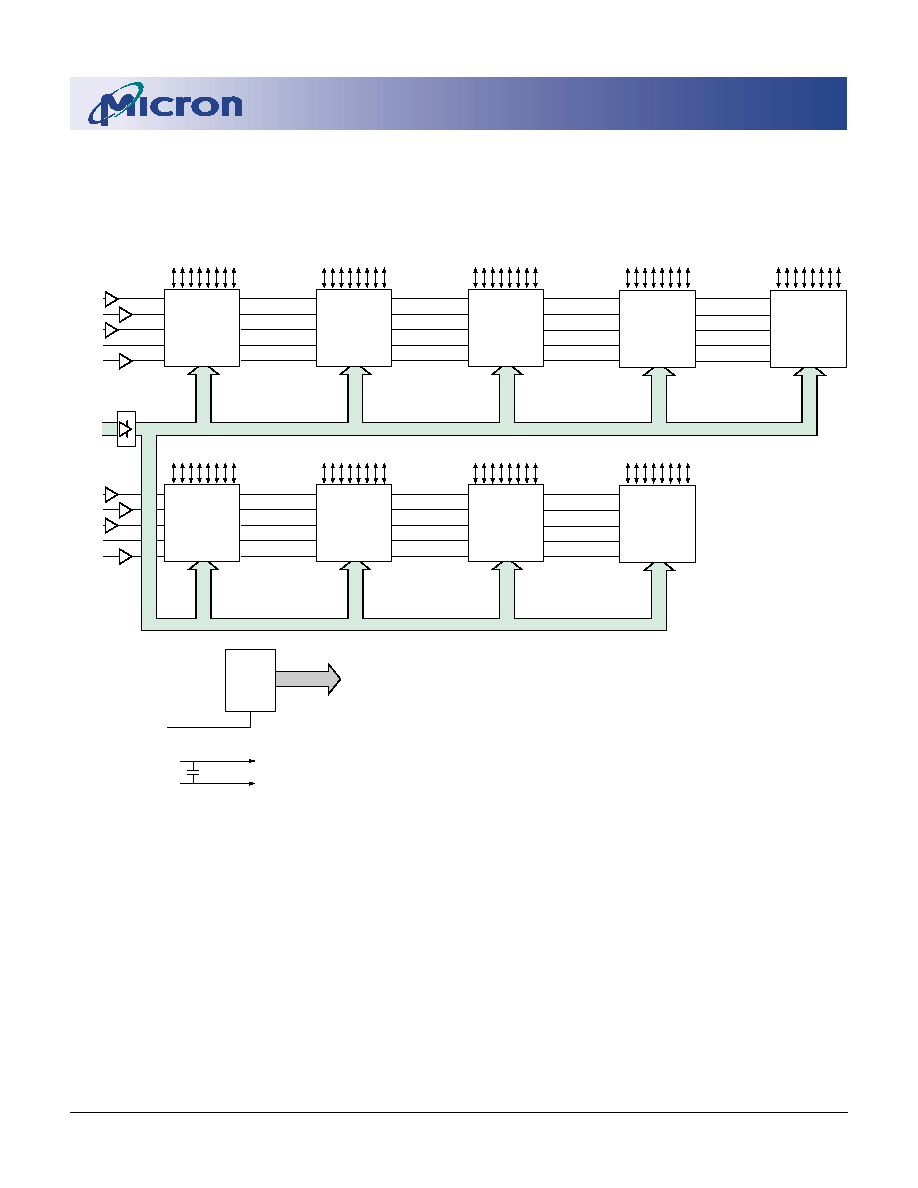
FUNCTIONAL BLOCK DIAGRAM
MT9LD(T)872(F)X (64MB)
NOTE: 1. All inputs with the exception of RAS# are redriven.
2. D = line buffers.
3. Reference designators in this diagram do not necessarily match the actual module.
D
D
D
A12-A1
D
D
D
OE0#
WE0#
CAS0#
RAS0#
D
D
A0
DQ0-DQ7
A1≠A11
DQ0-DQ7
DQ0-DQ7
A1≠A11
DQ0-DQ7
DQ0-DQ7
A1≠A11
A1≠A11
DQ0-DQ7
A1≠A11
A11
D
A1
A1≠A11
DQ0-DQ7
U0
A1≠A11
DQ0-DQ7
A1≠A11
DQ0-DQ7
DQ64-DQ71
DQ16-DQ23
DQ24-DQ31
DQ8-DQ15
DQ48-DQ55
DQ56-DQ63
DQ0-DQ7
DQ32-DQ39
DQ40-DQ47
U5
U4
U3
U2
U7
U8
U1
U6
A1≠A11
U0-U8 = MT4LC8M8C2DJ EDO PAGE MODE, SOJ, 4K REFRESH
PDE#
PD1-PD8
E#
PRESENCE
DETECT
GENERATOR
OE2#
WE2#
CAS4#
RAS2#
B0
A0
WE#
OE#
RAS#
CAS#
A0
WE#
OE#
RAS#
CAS#
A0
WE#
OE#
RAS#
CAS#
A0
WE#
OE#
RAS#
CAS#
A0
WE#
OE#
RAS#
CAS#
A0
WE#
OE#
RAS#
CAS#
A0
WE#
OE#
RAS#
CAS#
A0
WE#
OE#
RAS#
CAS#
A0
WE#
OE#
RAS#
CAS#
V
DD
V
SS
U0-U8, BUFFERS
U0-U8, BUFFERS
U0-U8 = MT4LC8M8C2TG EDO PAGE MODE, TSOP, 4K REFRESH
U0-U8 = MT4LC8M8P4DJ EDO PAGE MODE, SOJ, 8K REFRESH
U0-U8 = MT4LC8M8P4TG EDO PAGE MODE, TSOP, 8K REFRESH

4
8, 16, 32 Meg x 72 Buffered DRAM DIMMs
Micron Technology, Inc., reserves the right to change products or specifications without notice.
DM77_2.p65 ≠ Rev. 3/00
©2000, Micron Technology, Inc.
8, 16, 32 MEG x 72
BUFFERED DRAM DIMMs
FUNCTIONAL BLOCK DIAGRAM
MT18LD(T)1672(F)X (128MB)
NOTE: 1. All inputs with the exception of RAS# are redriven.
2. D = line buffers.
3. Reference designators in this diagram do not necessarily match the actual module.
D
D
D
D
OE0#
D
D
WE0#
CAS0#
OE2#
WE2#
CAS4#
A12-A1
RAS0#
RAS2#
D
A0
D
B0
A11
D
A1
PDE#
PD1-PD8
E#
PRESENCE-
DETECT
GENERATOR
A1≠A11
A0
WE#
OE#
RAS#
CAS#
A1≠A11
A0
WE#
OE#
RAS#
CAS#
A1≠A11
A0
WE#
OE#
RAS#
CAS#
A1≠A11
A0
WE#
OE#
RAS#
CAS#
A1≠A11
A0
WE#
OE#
RAS#
CAS#
A1≠A11
A0
WE#
OE#
RAS#
CAS#
A1≠A11
A0
WE#
OE#
RAS#
CAS#
A1≠A11
A0
WE#
OE#
RAS#
CAS#
A1≠A11
A0
WE#
OE#
RAS#
CAS#
A1≠A11
A0
WE#
OE#
RAS#
CAS#
A1≠A11
A0
WE#
OE#
RAS#
CAS#
A1≠A11
A0
WE#
OE#
RAS#
CAS#
A1≠A11
A0
WE#
OE#
RAS#
CAS#
A1≠A11
A0
WE#
OE#
RAS#
CAS#
A1≠A11
A0
WE#
OE#
RAS#
CAS#
A1≠A11
A0
WE#
OE#
RAS#
CAS#
DQ0-DQ3
U0
DQ0-DQ3
DQ0-DQ3
DQ0-DQ3
DQ0-DQ3
DQ0-DQ3
DQ0-DQ3
DQ0-DQ3
DQ0-DQ3
U9
DQ0-DQ3
A1≠A11
A0
WE#
OE#
RAS#
CAS#
U1
U2
U4
U5
U7
U3
U6
U8
U10
U11
U13
U14
U16
U17
U12
U15
DQ0-DQ3
DQ0-DQ3
DQ0-DQ3
DQ0-DQ3
DQ0-DQ3
DQ0-DQ3
DQ0-DQ3
DQ0-DQ3
DQ0-DQ3
DQ4-DQ7
DQ8-DQ11
DQ12-DQ15
DQ16-DQ19
DQ24-DQ27
DQ32-DQ35
DQ28-DQ31
DQ20-DQ23
DQ36-DQ39
DQ40-DQ43
DQ44-DQ47
DQ48-DQ51
DQ52-DQ55
DQ60-DQ63
DQ68-DQ71
DQ64-DQ67
DQ56-DQ59
A1≠A11
A0
WE#
OE#
RAS#
CAS#
V
DD
V
SS
U0-U17, BUFFERS
U0-U17, BUFFERS
U0-U17 = MT4LC16M4H9DJ EDO PAGE MODE, SOJ, 4K REFRESH
U0-U17 = MT4LC16M4H9TG EDO PAGE MODE, TSOP, 4K REFRESH
U0-U17 = MT4LC16M4G3DJ EDO PAGE MODE, SOJ, 8K REFRESH
U0-U17 = MT4LC16M4G3TG EDO PAGE MODE, TSOP, 8K REFRESH

5
8, 16, 32 Meg x 72 Buffered DRAM DIMMs
Micron Technology, Inc., reserves the right to change products or specifications without notice.
DM77_2.p65 ≠ Rev. 3/00
©2000, Micron Technology, Inc.
8, 16, 32 MEG x 72
BUFFERED DRAM DIMMs
FUNCTIONAL BLOCK DIAGRAM
MT36LD(T)3272(C)(F)X (256MB)
NOTE: 1. All inputs with the exception of RAS# are redriven.
2. D = line buffers.
3. Reference designators in this diagram do not necessarily match the actual module.
D
D
CAS1#
CAS5#
RAS1#
RAS3#
11
11
11
11
11
11
11
11
11
11
11
11
11
11
11
11
11
11
11
11
11
11
11
11
11
11
11
11
11
11
11
11
11
11
11
11
D
D
D
D
OE0#
D
D
WE0#
CAS0#
OE2#
WE2#
CAS4#
A11-A1
RAS0#
RAS2#
D
A0
D
B0
A11
D
A1
PDE#
PD1-PD8
E#
PRESENCE-
DETECT
GENERATOR
A1≠A11
A0
WE#
OE#
RAS#
CAS#
A1≠A11
A0
WE#
OE#
RAS#
CAS#
A1≠A11
A0
WE#
OE#
RAS#
CAS#
A1≠A11
A0
WE#
OE#
RAS#
CAS#
A1≠A11
A0
WE#
OE#
RAS#
CAS#
A1≠A11
A0
WE#
OE#
RAS#
CAS#
A1≠A11
A0
WE#
OE#
RAS#
CAS#
A1≠A11
A0
WE#
OE#
RAS#
CAS#
A1≠A11
A0
WE#
OE#
RAS#
CAS#
A1≠A11
A0
WE#
OE#
RAS#
CAS#
A1≠A11
A0
WE#
OE#
RAS#
CAS#
A1≠A11
A0
WE#
OE#
RAS#
CAS#
A1≠A11
A0
WE#
OE#
RAS#
CAS#
A1≠A11
A0
WE#
OE#
RAS#
CAS#
A1≠A11
A0
WE#
OE#
RAS#
CAS#
A1≠A11
A0
WE#
OE#
RAS#
CAS#
A1≠A11
A0
WE#
OE#
RAS#
CAS#
A1≠A11
A0
WE#
OE#
RAS#
CAS#
A1≠A11
A0
WE#
OE#
RAS#
CAS#
A1≠A11
A0
WE#
OE#
RAS#
CAS#
A1≠A11
A0
WE#
OE#
RAS#
CAS#
A1≠A11
A0
WE#
OE#
RAS#
CAS#
A1≠A11
A0
WE#
OE#
RAS#
CAS#
A1≠A11
A0
WE#
OE#
RAS#
CAS#
A1≠A11
A0
WE#
OE#
RAS#
CAS#
A1≠A11
A0
WE#
OE#
RAS#
CAS#
A1≠A11
A0
WE#
OE#
RAS#
CAS#
A1≠A11
A0
WE#
OE#
RAS#
CAS#
A1≠A11
A0
WE#
OE#
RAS#
CAS#
A1≠A11
A0
WE#
OE#
RAS#
CAS#
A1≠A11
A0
WE#
OE#
RAS#
CAS#
A1≠A11
A0
WE#
OE#
RAS#
CAS#
A1≠A11
A0
WE#
OE#
RAS#
CAS#
A1≠A11
A0
WE#
OE#
RAS#
CAS#
A1≠A11
A0
WE#
OE#
RAS#
CAS#
A1≠A11
A0
WE#
OE#
RAS#
CAS#
U18
U27
U9
DQ0-DQ3
U0
DQ0-DQ3
DQ0-DQ3
DQ0-DQ3
DQ0-DQ3
DQ0-DQ3
DQ0-DQ3
DQ0-DQ3
U19
U20
U22
U23
U25
U28
U29
U31
U32
U34
U35
U21
U30
U24
U33
U26
U10
U11
U13
U14
U16
U17
U12
U15
U1
U2
U4
U5
U7
U3
U6
U8
DQ0-DQ3
DQ0-DQ3
DQ0-DQ3
DQ0-DQ3
DQ0-DQ3
DQ0-DQ3
DQ0-DQ3
DQ0-DQ3
DQ0-DQ3
DQ0-DQ3
DQ0-DQ3
DQ0-DQ3
DQ0-DQ3
DQ0-DQ3
DQ0-DQ3
DQ0-DQ3
DQ0-DQ3
DQ0-DQ3
DQ0-DQ3
DQ0-DQ3
DQ0-DQ3
DQ0-DQ3
DQ0-DQ3
DQ0-DQ3
DQ0-DQ3
DQ0-DQ3
DQ0-DQ3
DQ0-DQ3
V
DD
V
SS
U0-U35, BUFFERS
U0-U35, BUFFERS
DQ0-DQ3
DQ4-DQ7
DQ8-DQ11
DQ12-DQ15
DQ16-DQ19
DQ24-DQ27
DQ32-DQ35
DQ28-DQ31
DQ20-DQ23
DQ36-DQ39
DQ40-DQ43
DQ44-DQ47
DQ48-DQ51
DQ52-DQ55
DQ60-DQ63
DQ68-DQ71
DQ64-DQ67
DQ56-DQ59
DQ0-DQ3
DQ4-DQ7
DQ8-DQ11
DQ12-DQ15
DQ16-DQ19
DQ24-DQ27
DQ32-DQ35
DQ28-DQ31
DQ20-DQ23
DQ36-DQ39
DQ40-DQ43
DQ44-DQ47
DQ48-DQ51
DQ52-DQ55
DQ60-DQ63
DQ68-DQ71
DQ64-DQ67
DQ56-DQ59
U0-U35 = MT4LC16M4T8DJ EDO PAGE MODE, SOJ, 4K REFRESH
U0-U35 = MT4LC16M4T8TG EDO PAGE MODE, TSOP, 4K REFRESH
U0-U35 = MT4LC16M4A7DJ EDO PAGE MODE, SOJ, 8K REFRESH
U0-U35 = MT4LC16M4A7TG EDO PAGE MODE, TSOP, 8K REFRESH