Document Outline
- Features
- Options
- Key SDRAM Component Timing Parameters
- Part Numbers
- 66-Pin AIMM (Front View)
- Introduction
- General Description
- Functional Block Diagram
- Pin Descriptions
- Commands
- Truth Table 1 - Commands and DQM Operation
- Burst Type
- Figure 1 Mode Register Definitions
- Table 1 Burst Definition
- Absolute Maximum Ratings
- DC Electrical Characterstics and Operating Conditions
- IDD Specifications and Conditions
- Capacitance
- AC Electrical Characteristicss
- AC Functional Characteristics
- Notes
- AIMM
1
1 Meg x 32 SDRAM AIMM
Micron Technology, Inc., reserves the right to change products or specifications without notice.
SD1C1X32AGP_A.p65 ≠ Rev. A; Pub. 5/01
©2001, Micron Technology, Inc.
1 MEG x 32
SDRAM AIMM
FEATURES
∑ AGP Inline Memory Module (AIMM)
∑ 4MB (1 Meg x 32)
∑ Single +3.3V ±0.3V power supply
∑ Fully synchronous; all signals registered on
positive edge of system clock
∑ Internal pipelined operation; column address can
be changed every clock cycle
∑ Internal banks for hiding row access/precharge
∑ Programmable burst lengths: 1, 2, 4, 8, or full page
∑ Auto Precharge and Auto Refresh Modes
∑ 64ms, 4,096-cycle refresh
∑ LVTTL-compatible inputs and outputs
∑ Fits in AGP port slot
OPTIONS
MARKING
∑ Timing (Cycle Time)
6ns
-6
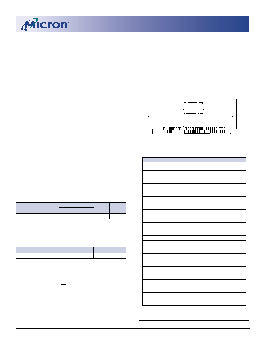
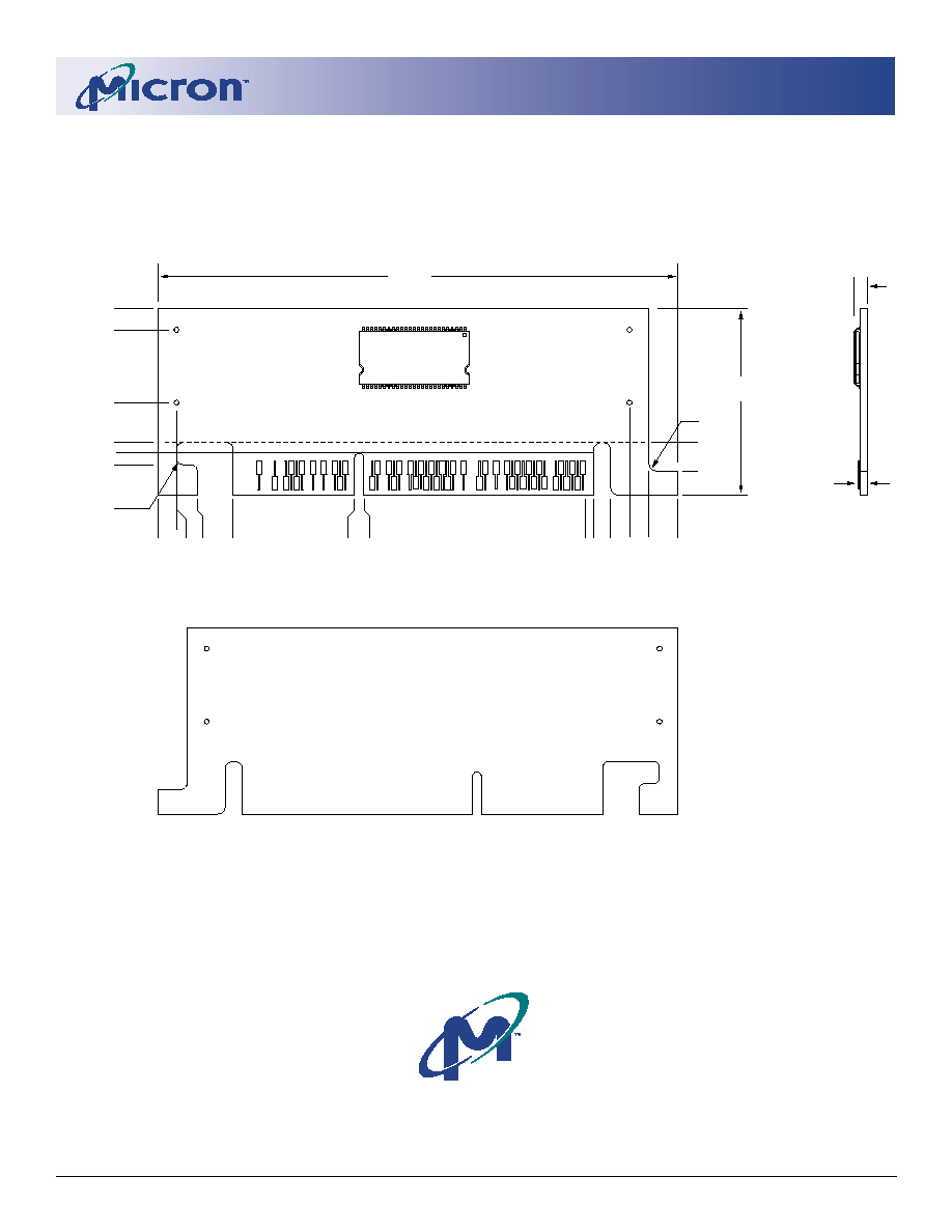
PIN ASSIGNMENT
66-Pin AIMM (Front View)
AGP MEMORY
MODULE
MT1LSDT132AGP
For the latest data sheet, please refer to the Micron
Web site:
www.micron.com/datasheets
KEY SDRAM COMPONENT TIMING
PARAMETERS
SPEED
CLOCK
ACCESS TIME
SETUP
HOLD
GRADE
FREQUENCY
CL = 3*
TIME
TIME
-6
166 MHz
5.5ns
1.5ns
1ns
*CL = CAS (READ) latency
PART NUMBERS
PART NUMBER
CONFIGURATION DEVICE PACKAGE
MT1LSDT132AGP-6_
1 Meg x 32
TSOP
NOTE: All part numbers end with a two-place code (not
shown), designating component and PCB revisions.
Consult factory for current revision codes. Example:
MT1LSDT132AGP-6E1.
PIN
B
A
PIN
B
A
1
NC
NC
34
V
DD
Q
V
DD
Q
2
NC
TYPEDET
35
DQ16
A0
3
NC
NC
36
DQ15
A9
4
NC
NC
37
GND
GND
5
GND
GND
38
DQ14
A11
6
NC
NC
39
DQ13
A8
7
NC
NC
40
V
DD
Q
V
DD
Q
8
DQ27
NC
41
DQ12
A10
9
VCC
VCC
42
NC
NC
10
DQ28
DQM3
43
GND
GND
11
DQ29
NC
44
NC
NC
12
DQ30
DQ24
45
VCC
VCC
13
GND
GND
46
DQ11
A7
14
NC
NC
47
V
DD
Q
CS#
15
DQ31
DQ25
48
NC
NC
16
VCC
VCC
49
GND
GND
17
DQM2
DQ26
50
NC
A6
18
NC
NC
51
DQ10
A1
19
GND
GND
52
V
DD
Q
V
DD
Q
20
DQ23
WE#
53
DQ9
A5
21
DQ22
FSEL
54
DQ8
A2
22
KEYWAY
KEYWAY
55
GND
GND
23
KEYWAY
KEYWAY
56
DQM1
A4
24
KEYWAY
KEYWAY
57
DQ0
A3
25
KEYWAY
KEYWAY
58
V
DD
Q
V
DD
Q
26
DQ21
TCLK0
59
NC
NC
27
DQ20
TCLK1
60
DQ1
DQ5
28
VCC
VCC
61
GND
GND
29
DQ19
CAS#
62
DQ2
DQ6
30
DQ18
NC
63
DQ3
DQ7
31
GND
GND
64
V
DD
Q
V
DD
Q
32
NC
NC
65
DQ4
DQM0
33
DQ17
RAS#
66
NC
NC
NOTE: Pins 22A≠25A and 22B≠25B are keyway pins.

2
1 Meg x 32 SDRAM AIMM
Micron Technology, Inc., reserves the right to change products or specifications without notice.
SD1C1X32AGP_A.p65 ≠ Rev. A; Pub. 5/01
©2001, Micron Technology, Inc.
1 MEG x 32
SDRAM AIMM
INTRODUCTION
This module is designed to be used in the AGP port
in PC motherboards and is intended to be a mid-level
cost between no added graphics memory and more
expensive AGP card solutions.
Accelerated Graphics Port (AGP) technology pro-
vides a dedicated, high-speed port for the movement
of large blocks of 3D texture data between the PC's
graphics controller and system memory. AGP is based
on a set of performance extensions or enhancements
to the PCI bus. AGP neither replaces nor diminishes
the necessity of PCI in the system. This high speed port
is physically, logically, and electrically independent of
the PCI bus. This module is targeted for AGP systems
supporting the AIMM socket.
GENERAL DESCRIPTION
The MT1LSDT132AGP is a high-speed CMOS, dy-
namic random-access, 4MB solid-state memory orga-
nized in a x32 configuration. This module is configured
as a single bank with a synchronous interface (all sig-
nals are registered on the positive edge of the clock
signal TCLK0). Read and write accesses to the SDRAM
module are burst oriented; accesses start at a selected
location and continue for a programmed number of
locations in a programmed sequence. Accesses begin
with the registration of an ACTIVE command, which is
then followed by a READ or WRITE command. The
address bits registered coincident with the ACTIVE
command are used to select the bank and row to be
accessed (BA0 selects the bank; A0-A11 select the row).
The address bits registered coincident with the READ
or WRITE command are used to select the starting col-
umn location for the burst access.
This module uses a single 64Mb 2 x 32 SDRAM com-
ponent. Note: only 4MB of the component are ad-
dressed by the AIMM design.
This module provides for a programmable READ or
WRITE burst terminate option. An auto precharge func-
tion may be enabled to provide a self-timed row
precharge that is initiated at the end of the burst se-
quence. This module uses an internal pipelined archi-
tecture to achieve high-speed operation. This archi-
tecture is compatible with the 2n rule of prefetch archi-
tectures, but it also allows the column address to be
changed on every clock cycle to achieve a high-speed,
fully random access. Precharging one bank while ac-
cessing the alternate bank will hide the PRECHARGE
cycles and provide seamless, high-speed, random-ac-
cess operation.
For more information regarding SDRAM operation,
refer to the 64Mb: x32 SDRAM data sheet.

3
1 Meg x 32 SDRAM AIMM
Micron Technology, Inc., reserves the right to change products or specifications without notice.
SD1C1X32AGP_A.p65 ≠ Rev. A; Pub. 5/01
©2001, Micron Technology, Inc.
1 MEG x 32
SDRAM AIMM
FUNCTIONAL BLOCK DIAGRAM
MT1LSDT132APG (4MB)
DQ8
DQ9
DQ10
DQ11
DQ12
DQ13
DQ14
DQ15
DQM1
U1
DQ0
DQ1
DQ2
DQ3
DQ4
DQ5
DQ6
DQ7
DQ0
DQ1
DQ2
DQ3
DQ4
DQ5
DQ6
DQ7
RAS#
CAS#
CS#
WE#
RAS#: SDRAM U1
CAS#: SDRAM U1
CS#: SDRAM U1
WE#: SDRAM U1
A0-A10, BA: SDRAM U1
A0-A11
V
DD
V
SS
SDRAM U1
SDRAM U1
DQ8
DQ9
DQ10
DQ11
DQ12
DQ13
DQ14
DQ15
DQM1
DQM0
DQM0
DQ24
DQ25
DQ26
DQ27
DQ28
DQ29
DQ30
DQ31
DQM3
DQ16
DQ17
DQ18
DQ19
DQ20
DQ21
DQ22
DQ23
DQ16
DQ17
DQ18
DQ19
DQ20
DQ21
DQ22
DQ23
DQM2
DQ24
DQ25
DQ26
DQ27
DQ28
DQ29
DQ30
DQ31
DQM3
U1 = MT48LC2M32B2TG SDRAM
CK1
U1
DQM2
4
1 Meg x 32 SDRAM AIMM
Micron Technology, Inc., reserves the right to change products or specifications without notice.
SD1C1X32AGP_A.p65 ≠ Rev. A; Pub. 5/01
©2001, Micron Technology, Inc.
1 MEG x 32
SDRAM AIMM
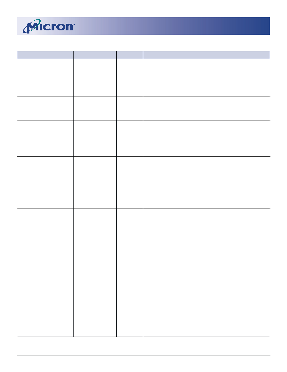
PIN DESCRIPTIONS
PIN NUMBERS
SYMBOL
TYPE
DESCRIPTION
A33, A29, A20
RAS#, CAS#, WE#
Input
Command Inputs: RAS#, CAS#, and WE# (along with
S0#-S3#) define the command being entered.
A26, A27
TCK0
Input
Clock: TCK0 is driven by the system clock. All SDRAM
input signals are sampled on the positive edge of CK.
CK also increments the internal burst counter and
controls the output registers.
A47
CS#
Input
Chip Select: CS# enables (registered LOW) and disables
(registered HIGH) the command decoder. All com-
mands are masked when CS# is registered HIGH. CS# is
considered part of the command code.
A10, A17, A56, A65
DQM0-DQM3
Input
Input/Output Mask: DQMB is an input mask signal for
write accesses and an output enable signal for read
accesses. Input data is masked when DQMB is sampled
HIGH during a WRITE cycle. The output buffers are
placed in a High-Z state (after a two-clock latency)
when DQMB is sampled HIGH during a READ cycle.
A35, A36, A38, A39, A41,
A0-A11/BA
Input
Address Inputs: A0-A11/BA are sampled during the
A46, A50, A51, A53, A54,
ACTIVE command (row-address A0-A10) and
A56, A57
READ/WRITE command (column-address A0-A7, with
A10 defining auto precharge) to select one location
out of the memory array in the respective bank. A10 is
sampled during a PRECHARGE command to determine
if both banks are to be precharged (A10 HIGH). The
address inputs also provide the op-code during a
LOAD MODE REGISTER command.
B57, B60, B62, B63, B65,
DQ0-DQ31
Input/
Data I/O: Data bus.
A60, A62, A63, B54, B53,
Output
B51, B46, B41, B39, B38,
B36, B35, B33, B30, B29,
B27, B26, B21, B20, A12,
A15, A17, B8, B10, B11,
B12, B15
A64, B64, B58, A52, B52,
V
SS
Supply
Ground.
B47, A40, B40, A34, B34
A45, B45, A28, B28, A25,
V
DD
Supply
Power Supply: +3.3V ±0.3V.
B25, A16, B16, A9, B9
A5, B5, A13, B13, A19,
GND
Supply
Ground
B19, A23, B23, A31, B31,
A61, B61, A55, B55, A49,
B49, A43, B43, A37, B37
A1, B1, B2, A3, B3, A4,
NC
≠
No Connects: These pins are not connected.
B4, A6, B6, A7, B7, A8,
A11, A14, B14, A18, B18,
A30, A32, B32, A42, B42,
A44, B44, A48, B48, B50,
A59, B59, A66, B66
5
1 Meg x 32 SDRAM AIMM
Micron Technology, Inc., reserves the right to change products or specifications without notice.
SD1C1X32AGP_A.p65 ≠ Rev. A; Pub. 5/01
©2001, Micron Technology, Inc.
1 MEG x 32
SDRAM AIMM
TRUTH TABLE ≠ Commands and DQM Operation
Note: 1
NAME (FUNCTION)
CS# RAS# CAS# WE# DQM
ADDR
DQs NOTES
COMMAND INHIBIT (NOP)
H
X
X
X
X
X
X
NO OPERATION (NOP)
L
H
H
H
X
X
X
ACTIVE (Select bank and activate row)
L
L
H
H
X
Bank/Row
X
3
READ (Select bank and column, and start READ burst)
L
H
L
H
L/H
8
Bank/Col
X
4
WRITE (Select bank and column, and start WRITE burst)
L
H
L
L
L/H
8
Bank/Col
Valid
4
BURST TERMINATE
L
H
H
L
X
X
Active
PRECHARGE (Deactivate row in bank or banks)
L
L
H
L
X
Code
X
5
AUTO REFRESH or SELF REFRESH
L
L
L
H
X
X
X
6, 7
(Enter self refresh mode)
LOAD MODE REGISTER
L
L
L
L
X
Op-Code
X
2
Write Enable/Output Enable
≠
≠
≠
≠
L
≠
Active
8
Write Inhibit/Output High-Z
≠
≠
≠
≠
H
≠
High-Z
8
appear following the Operation section; these tables
provide current state/next state information.
Commands
The Truth Table provides a quick reference of avail-
able commands. This is followed by a written descrip-
tion of each command. Three additional Truth Tables
NOTE: 1. CKE is HIGH for all commands shown except SELF REFRESH.
2. A0-A10 define the op-code written to the Mode Register.
3. A0-A10 provide row address, BA0 and BA1 determine which device bank is made active.
4. A0-A7 provide column address; A10 HIGH enables the auto precharge feature (nonpersistent), while
A10 LOW disables the auto precharge feature; BA0 and BA1 determine which device bank is being
read from or written to.
5. A10 LOW: BA0 and BA1 determine the device bank being precharged. A10 HIGH: All device banks
precharged and BA0 and BA1 are "Don't Care."
6. This command is AUTO REFRESH if CKE is HIGH; SELF REFRESH if CKE is LOW.
7. Internal refresh counter controls row addressing; all inputs and I/Os are "Don't Care" except for CKE.
8. Activates or deactivates the DQs during WRITEs (zero-clock delay) and READs (two-clock delay).
DQM0 controls DQ0-DQ7; DQM1 controls DQ8-DQ15; DQM2 controls DQ16-DQ23; and DQM3
controls DQ24-DQ31.

6
1 Meg x 32 SDRAM AIMM
Micron Technology, Inc., reserves the right to change products or specifications without notice.
SD1C1X32AGP_A.p65 ≠ Rev. A; Pub. 5/01
©2001, Micron Technology, Inc.
1 MEG x 32
SDRAM AIMM
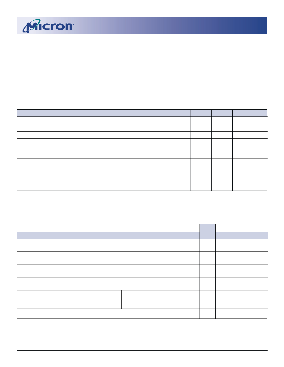
Figure 1
Mode Register Definition
BURST TYPE
Accesses within a given burst may be programmed
to be either sequential or interleaved; this is referred to
as the burst type and is selected via bit M3.
The ordering of accesses within a burst is deter-
mined by the burst length, the burst type and the start-
ing column address, as shown in Table 1.
0 0 0
0 0 1
0 1 0
0 1 1
1 0 0
1 0 1
1 1 0
1 1 1
M3 = 0
1
2
4
8
Reserved
Reserved
Reserved
Full Page
M3 = 1
1
2
4
8
Reserved
Reserved
Reserved
Reserved
Operating Mode
Standard operation
All other states reserved
0
-
0
-
Defined
-
0
1
Burst Type
Sequential
Interleave
CAS Latency
Reserved
Reserved
Reserved
3
Reserved
Reserved
Reserved
Reserved
0 0 0
0 0 1
0 1 0
0 1 1
1 0 0
1 0 1
1 1 0
1 1 1
Burst Length
M0
Burst length
CAS Latency
BT
A9
A7
A6
A5
A4
A3
A8
A2
A1
A0
Mode Register (Mx)
Address Bus
9
7
6
5
4
3
8
2
1
0
M1
M2
M3
M4
M5
M6
M6 - M0
M8
M7
Op Mode
A10
A11
10
Reserved*
11
Reserved*
WB
0
1
Write Burst Mode
Programmed Burst Length
Single Location Access
M9
1. *Should program
M11 = "0" to ensure
compatibility with
future devices.
2. BA0 = 0
Table 1
Burst Definition
Burst
Starting Column
Order of Accesses Within a Burst
Length
Address
Type = Sequential
Type = Interleaved
A0
2
0
0-1
0-1
1
1-0
1-0
A1 A0
0
0
0-1-2-3
0-1-2-3
4
0
1
1-2-3-0
1-0-3-2
1
0
2-3-0-1
2-3-0-1
1
1
3-0-1-2
3-2-1-0
A2 A1 A0
0
0
0
0-1-2-3-4-5-6-7
0-1-2-3-4-5-6-7
0
0
1
1-2-3-4-5-6-7-0
1-0-3-2-5-4-7-6
0
1
0
2-3-4-5-6-7-0-1
2-3-0-1-6-7-4-5
8
0
1
1
3-4-5-6-7-0-1-2
3-2-1-0-7-6-5-4
1
0
0
4-5-6-7-0-1-2-3
4-5-6-7-0-1-2-3
1
0
1
5-6-7-0-1-2-3-4
5-4-7-6-1-0-3-2
1
1
0
6-7-0-1-2-3-4-5
6-7-4-5-2-3-0-1
1
1
1
7-0-1-2-3-4-5-6
7-6-5-4-3-2-1-0
Full
n = A0-A7
Cn, Cn + 1, Cn + 2
Page
Cn + 3, Cn + 4...
Not Supported
(256)
(Location 0 -256)
...Cn - 1,
Cn...
NOTE:
1. For a burst length of two, A1-A7 select the block-
of-two burst; A0 selects the starting column
within the block.
2. For a burst length of four, A2-A7 select the block-
of-four burst; A0-A1 select the starting column
within the block.
3. For a burst length of eight, A3-A7 select the block-
of-eight burst; A0-A2 select the starting column
within the block.
4. For a full-page burst, the full row is selected and
A0-A7 select the starting column.
5. Whenever a boundary of the block is reached
within a given sequence above, the following
access wraps within the block.
6. For a burst length of one, A0-A7 select the unique
column to be accessed, and mode register bit M3
is ignored.
7
1 Meg x 32 SDRAM AIMM
Micron Technology, Inc., reserves the right to change products or specifications without notice.
SD1C1X32AGP_A.p65 ≠ Rev. A; Pub. 5/01
©2001, Micron Technology, Inc.
1 MEG x 32
SDRAM AIMM
ABSOLUTE MAXIMUM RATINGS*
Voltage on V
DD
Supply Relative to V
SS
....... -1V to +4.6V
Voltage on Inputs, NC or I/O Pins
Relative to V
SS
.......................................... -1V to +4.6V
Operating Temperature, T
A
(ambient) .. 0∞C to +70∞C
Storage Temperature (plastic) ........... -55∞C to +150∞C
Power Dissipation ........................................................ 1W
*Stresses greater than those listed under "Absolute
Maximum Ratings" may cause permanent damage to
the device. This is a stress rating only, and functional
operation of the device at these or any other conditions
above those indicated in the operational sections of
this specification is not implied. Exposure to absolute
maximum rating conditions for extended periods may
affect reliability.
DC ELECTRICAL CHARACTERISTICS AND OPERATING CONDITIONS
Notes: 1, 6 (V
DD
= +3.3V ±0.3V) (Notes following parameter tables.)
PARAMETER/CONDITION
SYMBOL
MIN
MAX
UNITS NOTES
SUPPLY VOLTAGE
V
DD
3.125
3.6
V
INPUT HIGH VOLTAGE: Logic 1; All inputs
V
IH
2
V
DD
+ 0.3
V
22
INPUT LOW VOLTAGE: Logic 0; All inputs
V
IL
-0.3
0.8
V
22
INPUT LEAKAGE CURRENT:
Any input 0V
V
IN
V
DD
I
I
-5
5
µA
(All other pins not under test = 0V)
OUTPUT LEAKAGE CURRENT:
I
OZ
-5
5
µA
DQs are disabled; 0V
V
OUT
V
DD
OUTPUT LEVELS:
V
OH
2.4
≠
V
Output High Voltage (I
OUT
= -4mA)
Output Low Voltage (I
OUT
= 4mA)
V
OL
≠
0.4
V
I
DD
SPECIFICATIONS AND CONDITIONS
Notes: 1, 6, 11, 13 (V
DD
= +3.3V ±0.3V) (Notes following parameter tables.)
PARAMETER/CONDITION
SYMBOL
-6
UNITS
NOTES
OPERATING CURRENT: Active Mode; Burst = 2; READ or WRITE;
I
DD
1
150
mA
3, 18,
t
RC =
t
RC (MIN); CAS latency = 3
19, 26
STANDBY CURRENT: Power-Down Mode;
I
DD
2
2
mA
CKE = LOW; All banks idle
STANDBY CURRENT: Active Mode; CS# = HIGH; CKE = HIGH;
I
DD
3
60
mA
3, 12,
All banks active after
t
RCD met; No accesses in progress
19, 26
OPERATING CURRENT: Burst Mode; Continuous burst;
I
DD
4
180
mA
3, 18,
READ or WRITE; All banks active; CAS latency = 3
19, 26
AUTO REFRESH CURRENT:
t
RFC =
t
RFC (MIN)
I
DD
5
225
mA
3, 12,
CAS latency = 3; CKE, CS# = HIGH
18, 19,
26,29
SELF REFRESH CURRENT: CKE
0.2V
I
DD
6
2
mA
4
MAX

8
1 Meg x 32 SDRAM AIMM
Micron Technology, Inc., reserves the right to change products or specifications without notice.
SD1C1X32AGP_A.p65 ≠ Rev. A; Pub. 5/01
©2001, Micron Technology, Inc.
1 MEG x 32
SDRAM AIMM
CAPACITANCE
(Notes following parameter tables.)
PARAMETER
SYMBOL
MIN
MAX UNITS NOTES
Input Capacitance: CKL
C
I
1
2.5
4
p F
2
Input Capacitance: All other input-only pins
C
I
2
2.5
4
p F
2
Input/Output Capacitance: DQs
C
IO
4
6.5
p F
2
AC ELECTRICAL CHARACTERISTICS
Notes: 5, 6, 8, 9, 11 (Notes following parameter tables.)
AC CHARACTERISTICS
-6
PARAMETER
SYMBOL
MIN
MAX
UNITS NOTES
Access time from CLK (pos. edge)
CL = 3
t
AC
5.5
ns
Address hold time
t
AH
1
ns
Address setup time
t
AS
1.5
ns
CLK high-level width
t
CH
2.5
ns
CLK low-level width
t
CL
2.5
ns
Clock cycle time
CL = 3
t
CK
6
ns
23
CKE hold time
t
CKH
1
ns
CKE setup time
t
CKS
1.5
ns
CS#, RAS#, CAS#, WE#, DQM hold time
t
CMH
1
ns
CS#, RAS#, CAS#, WE#, DQM setup time
t
CMS
1.5
ns
Data-in hold time
t
DH
1
ns
Data-in setup time
t
DS
1.5
ns
Data-out high-impedance time
CL = 3
t
HZ
5.5
ns
10
Data-out low-impedance time
t
LZ
1
ns
Data-out hold time
t
OH
2
ns
ACTIVE to PRECHARGE command
t
RAS
42
120,000
ns
ACTIVE to ACTIVE command period
t
RC
60
ns
AUTO REFRESH period
t
RFC
60
ns
ACTIVE to READ or WRITE delay
t
RCD
18
ns
Refresh period ( 4,096 cycles)
t
REF
64
ms
PRECHARGE command period
t
RP
18
ns
ACTIVE bank A to ACTIVE bank B command
t
RRD
12
ns
25
Transition time
t
T
0.3
1.2
ns
7
WRITE recovery time
t
WR
1 + 6ns
tCK
24
12
ns
Exit SELF REFRESH to ACTIVE command
t
XSR
70
ns
20

9
1 Meg x 32 SDRAM AIMM
Micron Technology, Inc., reserves the right to change products or specifications without notice.
SD1C1X32AGP_A.p65 ≠ Rev. A; Pub. 5/01
©2001, Micron Technology, Inc.
1 MEG x 32
SDRAM AIMM
AC FUNCTIONAL CHARACTERISTICS
Notes: 5, 6, 7, 8, 9, 11 (0∞C
T
A
+70∞C) (Notes following parameter tables.)
PARAMETER
SYMBOL
-6
UNITS NOTES
READ/WRITE command to READ/WRITE command
t
CCD
1
t
CK
17
CKE to clock disable or power-down entry mode
t
CKED
1
t
CK
14
CKE to clock enable or power-down exit setup mode
t
PED
1
t
CK
14
DQM to input data delay
t
DQD
0
t
CK
17
DQM to data mask during WRITEs
t
DQM
0
t
CK
17
DQM to data high-impedance during READs
t
DQZ
2
t
CK
17
WRITE command to input data delay
t
DWD
0
t
CK
17
Data-in to ACTIVE command
CL = 3
t
DAL
5
t
CK
15, 21
Data-in to PRECHARGE command
t
DPL
2
t
CK
16, 21
Last data-in to burst STOP command
t
BDL
1
t
CK
17
Last data-in to new READ/WRITE command
t
CDL
1
t
CK
17
Last data-in to PRECHARGE command
t
RDL
2
t
CK
16, 21
LOAD MODE REGISTER command to ACTIVE or REFRESH command
t
MRD
2
t
CK
26
Data-out to high-impedance from PRECHARGE command
CL = 3
t
ROH
3
t
CK
17

10
1 Meg x 32 SDRAM AIMM
Micron Technology, Inc., reserves the right to change products or specifications without notice.
SD1C1X32AGP_A.p65 ≠ Rev. A; Pub. 5/01
©2001, Micron Technology, Inc.
1 MEG x 32
SDRAM AIMM
NOTES
1.
All voltages referenced to V
SS
.
2.
This parameter is sampled. V
DD
, V
DD
Q = +3.3V;
f = 1 MHz, T
A
= 25∞C; pin under test biased at 1.4V.
3.
I
DD
is dependent on output loading and cycle rates.
Specified values are obtained with minimum cycle
time and the outputs open.
4.
Enables on-chip refresh and address counters.
5.
The minimum specifications are used only to indi-
cate cycle time at which proper operation over the
full temperature range (0∞C
T
A
+
70∞C) is en-
sured.
6.
An initial pause of 100µs is required after power-
up, followed by two AUTO REFRESH commands,
before proper device operation is ensured. (V
DD
and V
DD
Q must be powered up simultaneously. V
SS
and V
SS
Q must be at same potential.) The two AUTO
REFRESH command wake-ups should be repeated
any time the
t
REF refresh requirement is exceeded.
7.
AC characteristics assume
t
T = 1ns.
8.
In addition to meeting the transition rate specifi-
cation, the clock and CKE must transit between V
IH
and V
IL
(or between V
IL
and V
IH
) in a monotonic
manner.
9.
Outputs measured at 1.5V with equivalent load:
10.
t
HZ defines the time at which the output achieves
the open circuit condition; it is not a reference to
V
OH
or V
OL
. The last valid data element will meet
t
OH before going High-Z.
11. AC timing and I
DD
tests have V
IL
= .25 and V
IH
= 2.75,
with timing referenced to 1.5V crossover point.
12. Other input signals are allowed to transition no
more than once in any two-clock period and are
otherwise at valid V
IH
or V
IL
levels.
13. I
DD
specifications are tested after the device is prop-
erly initialized.
14. Timing actually specified by
t
CKS; clock(s) speci-
fied as a reference only at minimum cycle rate.
15. Timing actually specified by
t
WR plus
t
RP; clock(s)
specified as a reference only at minimum cycle rate.
16. Timing actually specified by
t
WR.
17. Required clocks are specified by JEDEC function-
ality and are not dependent on any timing param-
eter.
18. The I
DD
current will decrease as the CAS latency is
reduced. This is due to the fact that the maximum
cycle rate is slower as the CAS latency is reduced.
19. Address transitions average one transition every
two clocks.
20. CLK must be toggled a minimum of two times dur-
ing this period.
21. Based on
t
CK = 166 MHz for -6.
22. V
IH
overshoot: V
IH
(MAX) = V
DD
Q + 1.2V for a pulse
width
3ns, and the pulse width cannot be greater
than one third of the cycle rate. V
IL
undershoot:
V
IL
(MIN) = -1.2V for a pulse width
3ns, and the
pulse width cannot be greater than one third of the
cycle rate.
23. The clock frequency must remain constant during
access or precharge states (READ, WRITE, includ-
ing
t
WR, and PRECHARGE commands). CKE may
be used to reduce the data rate.
24. Auto precharge mode only.
25. JEDEC and PC100 specify three clocks.
26.
t
CK = 6ns for -6.
23.
Q
30pF
11
1 Meg x 32 SDRAM AIMM
Micron Technology, Inc., reserves the right to change products or specifications without notice.
SD1C1X32AGP_A.p65 ≠ Rev. A; Pub. 5/01
©2001, Micron Technology, Inc.
1 MEG x 32
SDRAM AIMM
AIMM
(4MB Version)
8000 S. Federal Way, P.O. Box 6, Boise, ID 83707-0006, Tel: 208-368-3900
E-mail: prodmktg@micron.com, Internet: http://www.micron.com, Customer Comment Line: 800-932-4992
Micron is a registered trademark and the Micron logo and M logo are trademarks of Micron Technology, Inc.
.125 (3.175)
MAX
.0630 ± .005
0
.143
.007
.157
.427
1.404
1.330
3.101
3.235
3.751
1.400
3.894
.510
.300
3.375
3.526
.465
.300
0
.550
.700
.350
.075 R
2x
.031 R (6x)
NOTE: 1. All dimensions in inches (millimeters).
FRONT
BACK