PRODUCTS AND SPECIFICATIONS DISCUSSED HEREIN ARE FOR EVALUATION AND REFERENCE PURPOSES ONLY AND ARE SUBJECT TO CHANGE BY
MICRON WITHOUT NOTICE. PRODUCTS ARE ONLY WARRANTED BY MICRON TO MEET MICRON'S PRODUCTION DATA SHEET SPECIFICATIONS.
09005aef80bcd58d
MT28C256564W18S_A.fm - Rev. A, Pub 6/03 EN
1
©2003 Micron Technology, Inc.
256Mb MULTIBANK BURST FLASH
32Mb/64Mb ASYNC/PAGE CellularRAM COMBO
ADVANCE
FLASH AND CellularRAM
TM
COMBO MEMORY
MT28C256532W18S
MT28C256564W18S
Low Voltage, Wireless Temperature
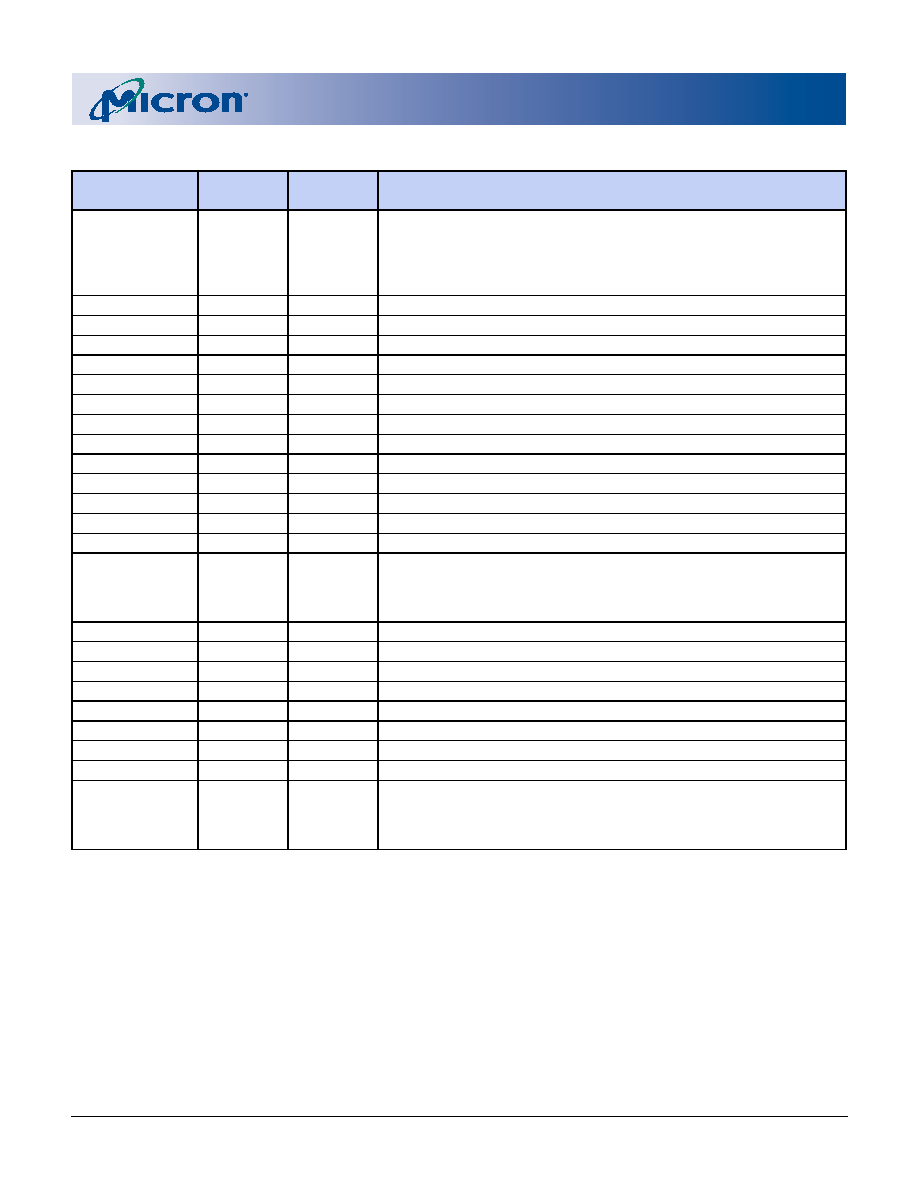
Features
∑ Stacked die Combo package
Includes two 128Mb Flash devices
Choice of either one 32Mb or one 64Mb
CellularRAM
‘ device
∑ Basic configuration
Flash
Flexible multibank architecture
8 Meg x 16 Async/Page/Burst interface
Support for true concurrent operations with
no latency
CellularRAM
Low-power, high-density design
2 Meg x 16 or 4 Meg x 16 configurations
Async/Page
∑ F_V
CC
, V
CC
Q, F_V
PP
, PS_V
CC
voltages
1.70V (MIN)/1.95V (MAX) F_V
CC
, PS_V
CC
1.70V (MIN)/2.24V (MAX) V
CC
Q
1.80V (TYP) F_V
PP
(in-system PROGRAM/ERASE)
12V ±5% (HV) F_V
PP
(in-house programming and
accelerated programming algorithm [APA]
activation)
∑ Asynchronous access time
Flash/CellularRAM access time: 60ns @ 1.70V V
CC
∑ Page Mode read access
Interpage read access: 60ns @ 1.8V F_V
CC
, PS_V
CC
Intrapage read access: 20ns @ 1.8V F_V
CC
, PS_V
CC
∑ Burst Mode Read Access
Max Operating Frequency: 66 MHz
Flash Initial Latency: 60ns @ 1.8V F_V
CC
/66 MHz
CellularRAM Initial Latency: 60ns @ 1.8V PS_V
CC
/66 MHz
t
ACLK: 11ns @ 1.8V Vcc
∑ Enhanced suspend options
ERASE-SUSPEND-to-READ within same bank
PROGRAM-SUSPEND-to-READ within same bank
ERASE-SUSPEND-to-PROGRAM within same bank
∑ Each Flash contains two 64-bit chip protection
registers for security purposes
∑ Flash PROGRAM/ERASE cycles
100,000 WRITE/ERASE cycles per block
∑ Cross-compatible command set support
Extended command set
Common Flash interface (CFI) compliant
Part Number Example:
MT28C256564W18S-705 BBWT
Options
Marking
∑ Timing
60ns
70ns
-60
-70
∑ Burst Frequency
66 MHz
54 MHz
6
5
∑ Boot Block Configuration
Top/Top
Top/Bottom
Bottom/Top
Bottom/Bottom
TT
TB
BT
BB
∑ Operating Voltage Range
PS_V
CC
1.70V≠1.95V
18
∑ Operating Temperature Range
Wireless Temperature (-25∞C to +85∞C)
WT
∑ Package
88-ball FBGA
(8 x 10 grid with eight support balls)
FT
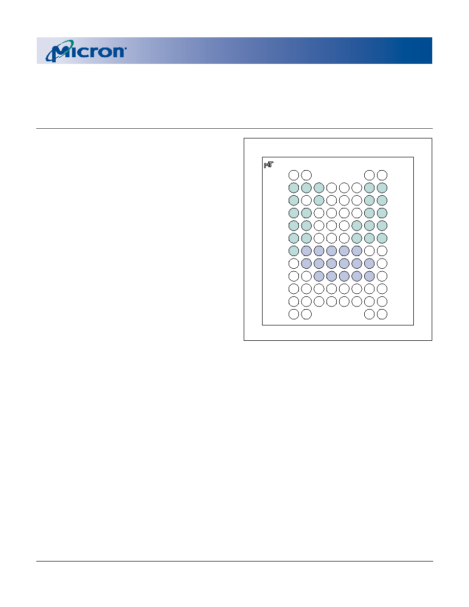
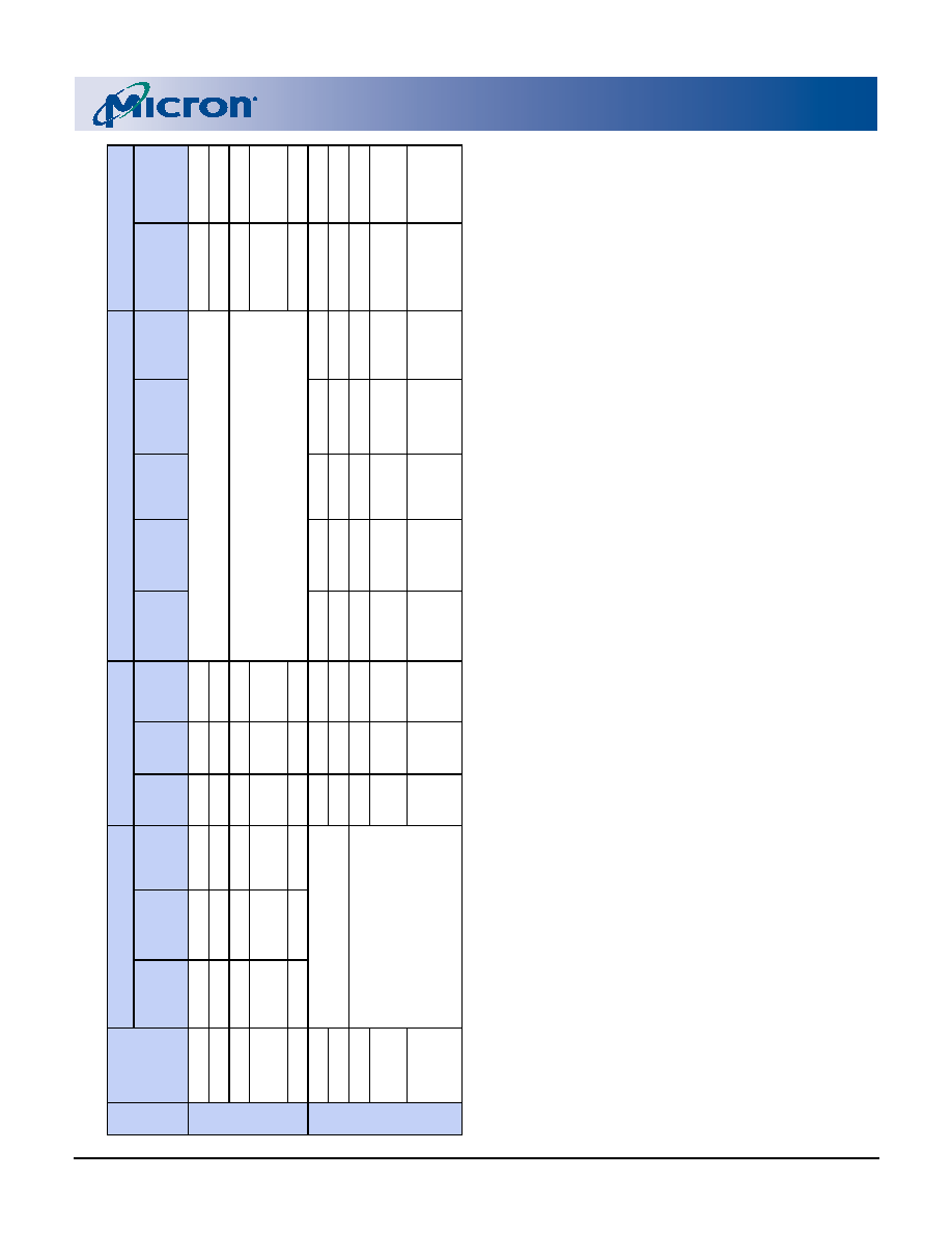
Figure 1: 88-Ball FBGA
A
B
C
D
E
F
G
H
J
K
L
M
1 2 3 4 5 6 7 8
Top View
(Ball Down)
PS_V
SS
PS_V
SS
F_V
PP
F_WP#
F_RP#
DQ10
DQ3
DQ11
NC
F_VCC
A19
A23
NC
NC
PS_UB#
DQ2
DQ1
DQ9
NC
V
CC
Q
NC
A4
A5
A3
A2
A1
A0
PS_OE#
NC
F_CE#1
PS_V
SS
NC
F_V
CC
CLK
PS_CE#
A20
A8
DQ13
DQ14
DQ6
F_V
CC
V
SS
Q
NC
A11
A12
A13
A15
A16
NC
NC
V
CC
Q
PS_ZZ#
PS_V
SS
NC
F_V
CC
NC
PS_WE#
ADV#
F_WE#
DQ5
DQ12
DQ4
PS_V
CC
PS_V
SS
NC
A18
PS_LB#
A17
A7
A6
DQ8
DQ0
F_OE#1
NC
V
SS
Q
NC
NC
A21
A22
A9
A10
A14
WAIT#
DQ7
DQ15
V
CC
Q
F_V
SS
NC

256Mb MULTIBANK BURST FLASH
32Mb/64Mb ASYNC/PAGE CellularRAM COMBO
ADVANCE
09005aef80bcd58d
Micron Technology, Inc., reserves the right to change products or specifications without notice.
MT28C256564W18S_A.fm - Rev. A, Pub 6/03 EN
2
©2003 Micron Technology. Inc.
Table of Contents
Features . . . . . . . . . . . . . . . . . . . . . . . . . . . . . . . . . . . . . . . . . . . . . . . . . . . . . . . . . . . . . . . . . . . . . . . . . . . . . . . . . . . . . . . . . . . . . .1
General Description . . . . . . . . . . . . . . . . . . . . . . . . . . . . . . . . . . . . . . . . . . . . . . . . . . . . . . . . . . . . . . . . . . . . . . . . . . . . . . . . . . .5
Flash Configurations . . . . . . . . . . . . . . . . . . . . . . . . . . . . . . . . . . . . . . . . . . . . . . . . . . . . . . . . . . . . . . . . . . . . . . . . . . . . . . . . . .5
Device Marking . . . . . . . . . . . . . . . . . . . . . . . . . . . . . . . . . . . . . . . . . . . . . . . . . . . . . . . . . . . . . . . . . . . . . . . . . . . . . . . . . . . . . . .8
Part Numbering Information . . . . . . . . . . . . . . . . . . . . . . . . . . . . . . . . . . . . . . . . . . . . . . . . . . . . . . . . . . . . . . . . . . . . . . . . . . .9
Boot Configurations . . . . . . . . . . . . . . . . . . . . . . . . . . . . . . . . . . . . . . . . . . . . . . . . . . . . . . . . . . . . . . . . . . . . . . . . . . . . . . . . . .11
MultiChip Packaging Considerations . . . . . . . . . . . . . . . . . . . . . . . . . . . . . . . . . . . . . . . . . . . . . . . . . . . . . . . . . . . . . . . . . . .11
Unique IDs, State Machines, and Registers. . . . . . . . . . . . . . . . . . . . . . . . . . . . . . . . . . . . . . . . . . . . . . . . . . . . . . . . . . . . . .11
Command Codes. . . . . . . . . . . . . . . . . . . . . . . . . . . . . . . . . . . . . . . . . . . . . . . . . . . . . . . . . . . . . . . . . . . . . . . . . . . . . . . . . . . . .11
READ Operation . . . . . . . . . . . . . . . . . . . . . . . . . . . . . . . . . . . . . . . . . . . . . . . . . . . . . . . . . . . . . . . . . . . . . . . . . . . . . . . . . . . . .11
Flash Reset . . . . . . . . . . . . . . . . . . . . . . . . . . . . . . . . . . . . . . . . . . . . . . . . . . . . . . . . . . . . . . . . . . . . . . . . . . . . . . . . . . . . . . . . . .11
Power Consumption. . . . . . . . . . . . . . . . . . . . . . . . . . . . . . . . . . . . . . . . . . . . . . . . . . . . . . . . . . . . . . . . . . . . . . . . . . . . . . . . . .11
Flash Electrical Specifications . . . . . . . . . . . . . . . . . . . . . . . . . . . . . . . . . . . . . . . . . . . . . . . . . . . . . . . . . . . . . . . . . . . . . . . .13
Data Sheet Designation . . . . . . . . . . . . . . . . . . . . . . . . . . . . . . . . . . . . . . . . . . . . . . . . . . . . . . . . . . . . . . . . . . . . . . . . . . . . . . .20
Revision History. . . . . . . . . . . . . . . . . . . . . . . . . . . . . . . . . . . . . . . . . . . . . . . . . . . . . . . . . . . . . . . . . . . . . . . . . . . . . . . . . . . . . .21

256Mb MULTIBANK BURST FLASH
32Mb/64Mb ASYNC/PAGE CellularRAM COMBO
ADVANCE
09005aef80bcd58d
Micron Technology, Inc., reserves the right to change products or specifications without notice.
MT28C256564W18S_A.fm - Rev. A, Pub 6/03 EN
3
©2003 Micron Technology. Inc.
List of Figures
Figure 1:
88-Ball FBGA . . . . . . . . . . . . . . . . . . . . . . . . . . . . . . . . . . . . . . . . . . . . . . . . . . . . . . . . . . . . . . . . . . . . . . . . . . . . .1
Figure 2:
Flash Memory Map . . . . . . . . . . . . . . . . . . . . . . . . . . . . . . . . . . . . . . . . . . . . . . . . . . . . . . . . . . . . . . . . . . . . . . .6
Figure 3:
Block Diagram . . . . . . . . . . . . . . . . . . . . . . . . . . . . . . . . . . . . . . . . . . . . . . . . . . . . . . . . . . . . . . . . . . . . . . . . . . . .7
Figure 4:
Part Number Chart . . . . . . . . . . . . . . . . . . . . . . . . . . . . . . . . . . . . . . . . . . . . . . . . . . . . . . . . . . . . . . . . . . . . . . . .9
Figure 5:
88-Ball FBGA . . . . . . . . . . . . . . . . . . . . . . . . . . . . . . . . . . . . . . . . . . . . . . . . . . . . . . . . . . . . . . . . . . . . . . . . . . . .20

256Mb MULTIBANK BURST FLASH
32Mb/64Mb ASYNC/PAGE CellularRAM COMBO
ADVANCE
09005aef80bcd58d
Micron Technology, Inc., reserves the right to change products or specifications without notice.
MT28C256564W18S_A.fm - Rev. A, Pub 6/03 EN
4
©2003 Micron Technology. Inc.
List of Tables
Table 1:
Cross-Reference for Abbreviated Device Marks. . . . . . . . . . . . . . . . . . . . . . . . . . . . . . . . . . . . . . . . . . . . . . .8
Table 2:
Valid Part Number Combinations. . . . . . . . . . . . . . . . . . . . . . . . . . . . . . . . . . . . . . . . . . . . . . . . . . . . . . . . . . .9
Table 3:
Ball Descriptions. . . . . . . . . . . . . . . . . . . . . . . . . . . . . . . . . . . . . . . . . . . . . . . . . . . . . . . . . . . . . . . . . . . . . . . . .10
Table 4:
Possible Boot Configurations for Flash Die . . . . . . . . . . . . . . . . . . . . . . . . . . . . . . . . . . . . . . . . . . . . . . . . .11
Table 5:
Truth Table. . . . . . . . . . . . . . . . . . . . . . . . . . . . . . . . . . . . . . . . . . . . . . . . . . . . . . . . . . . . . . . . . . . . . . . . . . . . . .12
Table 6:
Absolute Maximum Ratings
1
. . . . . . . . . . . . . . . . . . . . . . . . . . . . . . . . . . . . . . . . . . . . . . . . . . . . . . . . . . . . . .13
Table 7:
Recommended Operating Conditions . . . . . . . . . . . . . . . . . . . . . . . . . . . . . . . . . . . . . . . . . . . . . . . . . . . . . .13
Table 8:
Capacitance . . . . . . . . . . . . . . . . . . . . . . . . . . . . . . . . . . . . . . . . . . . . . . . . . . . . . . . . . . . . . . . . . . . . . . . . . . . . .13
Table 9:
DC Characteristics . . . . . . . . . . . . . . . . . . . . . . . . . . . . . . . . . . . . . . . . . . . . . . . . . . . . . . . . . . . . . . . . . . . . . . .14
Table 10:
CFI . . . . . . . . . . . . . . . . . . . . . . . . . . . . . . . . . . . . . . . . . . . . . . . . . . . . . . . . . . . . . . . . . . . . . . . . . . . . . . . . . . . . .16

256Mb MULTIBANK BURST FLASH
32Mb/64Mb ASYNC/PAGE CellularRAM COMBO
ADVANCE
09005aef80bcd58d
Micron Technology, Inc., reserves the right to change products or specifications without notice.
MT28C256564W18S_A.fm - Rev. A, Pub 6/03 EN
5
©2003 Micron Technology. Inc.
General Description
The MT28C256532W18S/MT28C256564W18S com-
bination Flash and CellularRAM is a high-performance,
high-density, memory solution that can significantly
improve system performance. The Flash architecture
features a multipartition configuration that supports
READ-while-PROGRAM/ERASE operations with no
latency. An 8Mb partition size enables optimal design
flexibility.
Two Flash devices are stacked to achieve the 256Mb
density. Both Flash die share a dedicated CE# and OE#
control.
The MT28C256532W18S/MT28C256564W18S
stacked Flash device enables soft protection for blocks,
as read only, by configuring soft protection registers
with dedicated command sequences. For security pur-
poses, two user-programmable 64-bit chip protection
registers are provided for each Flash device.
The embedded WORD PROGRAM and BLOCK
ERASE functions are fully automated by an on-chip
write state machine (WSM). An on-chip device status
register can be used to monitor the WSM status and
determine the progress of the PROGRAM/ERASE tasks.
Each Flash device has a read configuration register
(RCR) that defines how the Flash interacts with the
memory bus. For device specifications and additional
documentation concerning Flash and CellularRAM fea-
tures, please refer to the MT28F1284W18 data sheet at
www.micron.com/flash
and the MT45W2MW16PFA and
MT45W4MW16PFA data sheets at
http://
www.micron.com/cellularram
.
The CellularRAM architecture features high-speed
CMOS, dynamic random-access memories developed for
low-power portable applications The CellularRAM device
is available in either 32Mb or 64Mb densities.
To operate seamlessly on a burst Flash bus, Cellular-
RAM products have incorporated a transparent self-
refresh mechanism. The hidden refresh requires no
additional support from the system memory controller
and has no significant impact on device read/write per-
formance.
The refresh configuration register (CR) is used to con-
trol how refresh is performed on the DRAM array. These
registers are automatically loaded with default settings
during power-up and can be updated any time during
normal operation. Special attention has been focused
on standby current consumption during self-refresh.
CellularRAM products include three system-acces-
sible mechanisms used to minimize standby current.
Partial array refresh (PAR) limits refresh to the portion
of the memory array being used. Temperature com-
pensated refresh (TCR) is used to adjust the refresh
rate according to the ambient temperature. The
refresh rate can be decreased to lower temperatures to
minimize current consumption during standby. Deep
sleep mode halts the refresh operation altogether and
is used when no vital information is stored in the
device. These three refresh mechanisms are adjusted
through the CR.
Please refer to Micron's Web site
www.micron.com/
flash
for the latest MT28F1284W18
Flash data sheet
sheet and
http://www.micron.com/cellularram
for the
latest MT45W2MW16PFA and MT45W4MW16PFA Cel-
lularRAM data sheet.
Flash Configurations
Each Flash memory implements a multibank archi-
tecture (16 banks of 8Mb each) to allow concurrent
operations. Any address within a block address range
selects that block for the required READ, PROGRAM, or
ERASE operation.
Each Flash memory features eight 8K-word sectors
(8 x 65,536 bits), designated as parameter blocks, and
the remaining part is organized in main blocks of 64K
words each (524,288 bits). The parameter blocks are
addressed either by the low order addresses (bottom
boot) or by the higher order addresses (top boot).
The two Flash devices can be supplied with any
combination of top or bottom boot (e.g., top/top, bot-
tom/bottom, top/bottom, or bottom/top). Please see
Figures 2 and 3 for more information.
256Mb MULTIBANK BURST FLASH
32Mb/64Mb ASYNC/PAGE CellularRAM COMBO
ADVANCE
09005aef80bcd58d
Micron Technology, Inc., reserves the right to change products or specifications without notice.
MT28C256564W18S_A.fm - Rev. A, Pub 6/03 EN
6
©2003 Micron Technology. Inc.
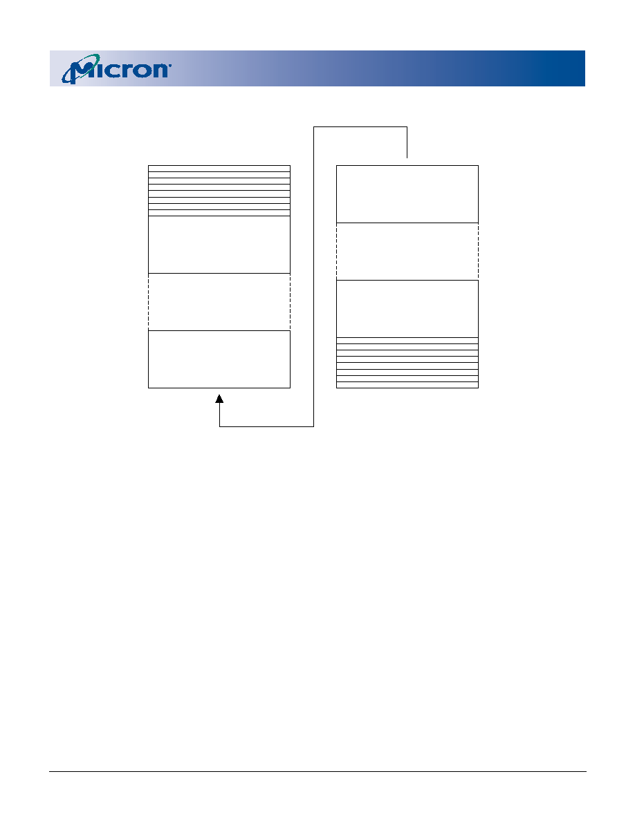
Figure 2: Flash Memory Map
NOTE:
Figure 2 shows a BT (bottom/top) dual Flash configuration.
Parameter
Blocks ≠
Top Boot
(128Mb to 256Mb)
Main
Main
Main
Parameter
Blocks ≠
Bottom Boot
(0Mb to 128Mb)
Main
Main
Main
256Mb MULTIBANK BURST FLASH
32Mb/64Mb ASYNC/PAGE CellularRAM COMBO
ADVANCE
09005aef80bcd58d
Micron Technology, Inc., reserves the right to change products or specifications without notice.
MT28C256564W18S_A.fm - Rev. A, Pub 6/03 EN
7
©2003 Micron Technology. Inc.
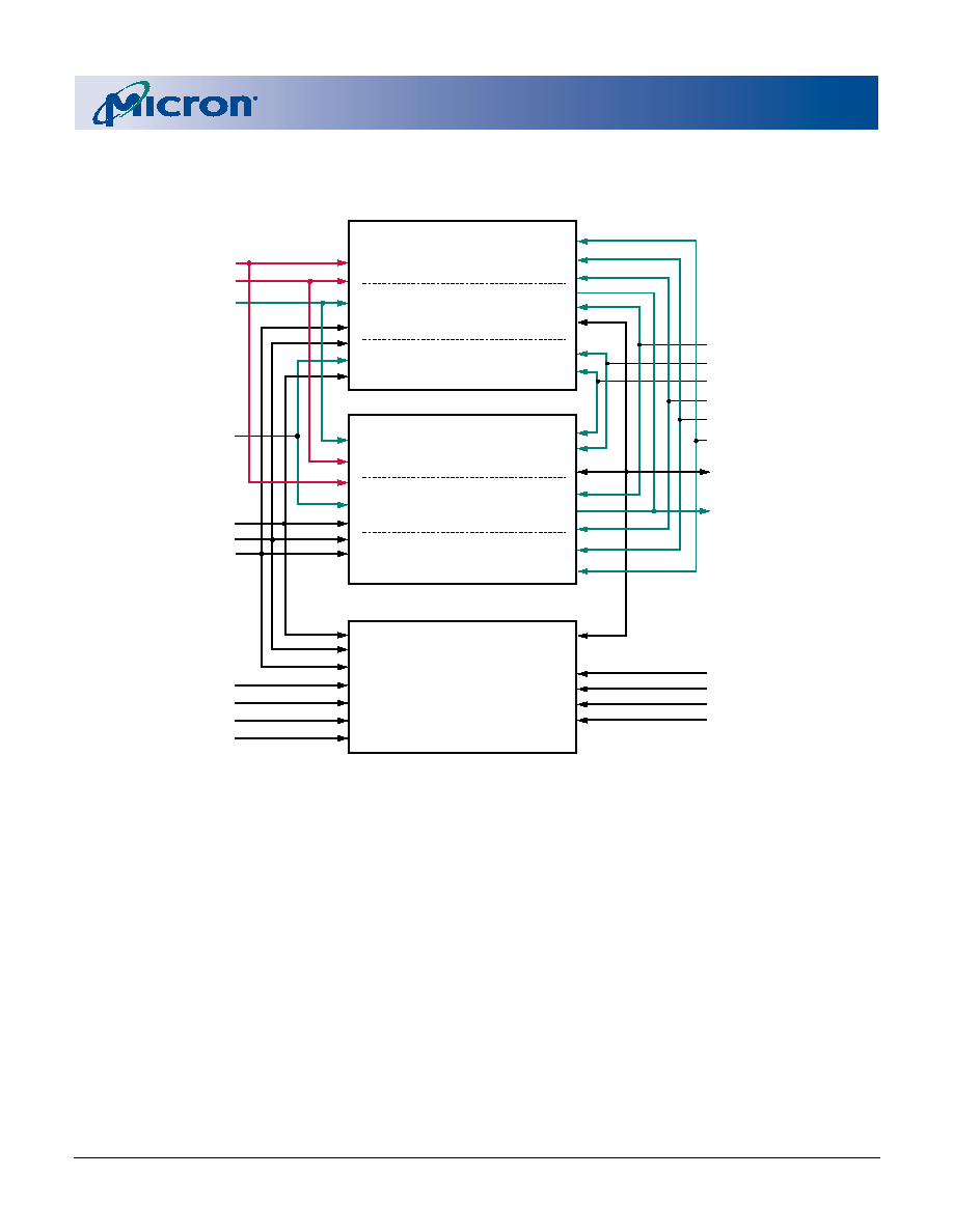
Figure 3: Block Diagram
PS_OE#
PS_ZZ#
PS_CE#
PS_WE#
DQ0≠DQ15
A0≠A23
F_WE#
CLK
F_WP#
WAIT#
FLASH #1
CellularRAM
F_RP#
PS_UB#
PS_LB#
8,192K x 16
2,048K x 16
4,096K x 16
Bank 0
Bank 15
PS_V
CC
F_OE#
F_CE#
ADV#
PS_V
SS
FLASH #2
8,192K x 16
Bank 16
Bank 31
V
CC
Q
V
SS
Q
F_V
CC
F_V
SS
F_V
PP

256Mb MULTIBANK BURST FLASH
32Mb/64Mb ASYNC/PAGE CellularRAM COMBO
ADVANCE
09005aef80bcd58d
Micron Technology, Inc., reserves the right to change products or specifications without notice.
MT28C256564W18S_A.fm - Rev. A, Pub 6/03 EN
8
©2003 Micron Technology. Inc.
Device Marking
Due to the size of the package, the Micron
‚
stan-
dard part number is not printed on the top of each
device. Instead, an abbreviated device mark com-
prised of a five-digit alphanumeric code is used. The
abbreviated device marks are cross-referenced to the
Micron part numbers in Table 1.
Table 1:
Cross-Reference for Abbreviated Device Marks
PRODUCT PART NUMBER
PRODUCT
MARKING
SAMPLE
MARKING
MECHANICAL
MARKING
MT28C256532W18SFT-705 BTWT
FW636
FX636
FY636
MT28C256532W18SFT-705 TTWT
FW641
FX641
FY641
256Mb MULTIBANK BURST FLASH
32Mb/64Mb ASYNC/PAGE CellularRAM COMBO
ADVANCE
09005aef80bcd58d
Micron Technology, Inc., reserves the right to change products or specifications without notice.
MT28C256564W18S_A.fm - Rev. A, Pub 6/03 EN
9
©2003 Micron Technology. Inc.
Part Numbering Information
Micron's low-power devices are available with sev-
eral different combinations of features (see Figure 4).
Valid combinations of features and their correspond-
ing part numbers are listed in Table 2.
Figure 4: Part Number Chart
MT 28C 2565 64 W18 S FT -70 5 BB WT ES
Micron Technology
Flash Family
28C = Dual-Supply Flash/CellularRAM Combo
Density/Organization/Banks
256 = 256Mb (8,192K x 16)
bank x = 5 Multibank 32 Banks
(all banks have the same dimensions)
Access Time
-60 = 60ns
-70 = 70ns
CellularRAM Density
64 = 64Mb CellularRAM (4 Meg x 16)
32 = 32Mb CellularRAM (2 Meg x 16)
Flash Read Mode Operation
W = Flash Async/Page/Burst Read
Package Code
FT = 80-ball FBGA with eight
support balls (8 x 10 grid)
Operating Temperature Range
WT = Wireless (-25∫C to +85∫C)
Burst Mode Frequency
5 = 54 MHz
6 = 66 MHz
Boot Block Starting Address
BB = Bottom boot/Bottom boot
BT = Bottom boot/Top boot
TT = Top boot/Top boot
TB = Top boot/Bottom boot
Operating Voltage Range
18 = 1.7V≠1.95V Vcc
CE Select/Special Mark
S = Single CE Flash with Asynchronous PSRAM
Production Status
Blank = Production
ES = Engineering Samples
MS = Mechanical Samples
Table 2:
Valid Part Number Combinations
PART NUMBER
ACCESS TIME
(ns)
BOOT BLOCK STARTING
ADDRESS
BURST FREQUENCY
(MHz)
MT28C256532W18SFT-705 BTWT
-70
Bottom/Top
54
MT28C256532W18SFT-705 TTWT
-70
Top/Top
54
256Mb MULTIBANK BURST FLASH
32Mb/64Mb ASYNC/PAGE CellularRAM COMBO
ADVANCE
09005aef80bcd58d
Micron Technology, Inc., reserves the right to change products or specifications without notice.
MT28C256564W18S_A.fm - Rev. A, Pub 6/03 EN
10
©2003 Micron Technology. Inc.
Table 3:
Ball Descriptions
88-BALL FBGA
NUMBERS
SYMBOL
TYPE
DESCRIPTIONS
B1, B2, B3, B7, B8,
C1, C3, C7, C8, D1,
D2, D7, D8, E1, E2,
E6, E7, E8, F1, F2,
F6, F7, F8, G1
A0≠A23
Input
Addresses:
Flash: A0≠A23
CellularRAM: A0≠A21 (64Mb)
CellularRAM: A0≠A20 (32Mb)
K1
F_CE#
Input
Flash Chip Enable
J2
F_OE#
Input
Flash Output Enable
F5
F_WE#
Input
Flash Write Enable
E4
F_WP#
Input
Flash Write Protect
C2
PS_LB#
Input
CellularRAM Lower Byte Control
F3
PS_UB#
Input
CellularRAM Upper Byte Control
D5
PS_WE#
Input
CellularRAM Write Enable
H1
PS_OE#
Input
CellularRAM Output Enable
D6
PS_CE#
Input
CellularRAM Chip Enable
K8
PS_ZZ#
Input
CellularRAM Deep Sleep Mode and Configuration Mode
E5
ADV#
Input
Flash Address Valid (Burst operation only)
C6
CLK
Input
Flash Clock (Burst operation only)
F4
F_RP#
Input
Flash Reset
G2, G3, G4, G5,
G6, H2, H3, H4,
H5, H6, H7, J3, J4,
J5, J6, J7
DQ0≠DQ15
I/O
Flash/CellularRAM Data Input/Output
G7
WAIT#
Output
Flash/ WAIT#
L7
F_V
SS
Supply
Flash Core Ground
D4
F_V
PP
Supply
Flash V
PP
K6
F_V
CC
Supply
Flash Core Power Supply
L5
PS_V
SS
Supply
CellularRAM Core Ground
K5
PS_V
CC
Supply
CellularRAM Core Power supply
K7
V
CC
Q
Supply
Flash/CellularRAM I/O supply
L6
V
SS
Q
Supply
Flash/CellularRAM I/O ground
A1, A2, A7, A8, C5,
D3, E3, G8, H8, J1,
K2, K3, K4, M1,
M2, M7, M8
NC
≠
No Connect

256Mb MULTIBANK BURST FLASH
32Mb/64Mb ASYNC/PAGE CellularRAM COMBO
ADVANCE
09005aef80bcd58d
Micron Technology, Inc., reserves the right to change products or specifications without notice.
MT28C256564W18S_A.fm - Rev. A, Pub 6/03 EN
11
©2003 Micron Technology. Inc.
Boot Configurations
The possible configurations for Flash die are shown
in Table 4 below. This table shows the possible config-
urations of the two Flash devices for either top boot or
bottom boot.
MultiChip Packaging Considerations
Multichip packaging presents unique chal-
lenges when controlling complex memory devices.
The MT28C256532W18 and MT28C256564W18
devices combine two Micron Flash devices with a
single CellularRAM device.
Unique IDs, State Machines, and
Registers
Each Flash device has a separate command state
machine (CSM) and status register (SR) and read con-
figuration register (RCR). The RCR settings are sepa-
rate and can be different for the upper and lower
device. Each Flash device has its own OTP, CFI, and
device code. Depending on the boot configuration of
each Flash device, the OTP, CFI, and device code infor-
mation may differ.
The CellularRAM device has a refresh configuration
register (CR) that defines how the device performs self
refresh.
Command Codes
All Flash command codes are independent
within each device. Care must be taken when
crossing the array boundary between the upper
and lower Flash device and the CellularRAM
device to ensure that only one device is enabled at
one time.
In a two-cycle command sequence such as word
program (0x40/data), it is required that both com-
mands be issued to the same device.
It is not recommended that READ and ERASE
operations occur simultaneously on two devices.
READ Operation
Page and burst read modes are limited to the
address boundaries of each device. A new page/ burst
operation must be started when crossing a device
boundary.
Flash Reset
The reset control is shared by both Flash die.
Bringing RST# conrol LOW will reset both the
upper and lower device.
Power Consumption
Multiple chip packaging requires that power
calculations consider the active operation of the
upper and lower Flash device as well as that of the
CellularRAM device. Total power consumed will
be the sum of the currents associated with the
state of each device. Table 10 on page 14 shows the
power consumption specifications.
Table 4:
Possible Boot Configurations
for Flash Die
CONFIGURATION
F_CE1#
ORDER CODE
Top/Top
Top
TT
Bottom/Top
Bottom
BT
Top/Bottom
Top
TB
Bottom/Bottom
Bottom
BB
256Mb MU
L
T
IBAN
K
BURST FL
ASH
32
Mb/
6
4M
b ASYNC/
PAGE C
e
ll
ularRAM
COM
B
O
ADV
ANCE
09005
aef80b
c
d
5
8
d
M
i
c
ro
n
Tec
h
n
o
l
o
g
y
,
I
n
c
.
,
r
e
serv
es
th
e
ri
g
h
t t
o
c
h
a
n
g
e
p
r
o
d
u
c
t
s
o
r
sp
ec
i
f
i
c
at
i
o
n
s
w
i
th
o
u
t
n
o
ti
c
e
.
MT28
C
25656
4W18S
_
A
.
f
m
-
R
e
v
.
A,
Pu
b
6/
0
3
EN
12
©2
003,
Mi
c
r
o
n
Tec
h
n
o
l
o
g
y
,
I
n
c
.
Table 5:
Truth Table
MODES
FLASH SIGNALS
SHARED SIGNALS
CellularRAM SIGNALS
MEMORY OUPUT
F_CE#
F_OE#
F_WE#
F_RP# ADV#
WAIT#
PS_CE#
PS_CRE# PS_OE# PS_UB/LB PS_WE#
MEMORY
BUS
CONTROL
D0≠D15
FLA
SH
F
_
CE#
Read
L
L
H
H
L
Valid
CellularRAM must be in High-Z
Flash
D
OUT
Write
L
H
L
H
L
Valid
Flash
D
IN
Standby
H
X
X
H
X
X
CellularRAM any mode allowable
Other
High-Z
Output
Disable
L
H
H
H
X
X
Other
High-Z
Reset
X
X
X
L
X
X
None
High-Z
CellularRAM
Read
Flash must be in High-Z
X
L
Valid
L
H
L
L
H
PSRAM
D
OUT
Write
X
L
Valid
L
H
H
L
L
PSRAM
D
IN
Standby
Flash any mode allowable
X
X
X
H
H
X
X
X
Other
High-Z
Output
Disable
X
X
X
L
H
H
X
X
Other
High-Z
Deep
Sleep
Mode
X
X
X
H
L
X
X
X
Other
High-Z
256Mb MULTIBANK BURST FLASH
32Mb/64Mb ASYNC/PAGE CellularRAM COMBO
ADVANCE
09005aef80bcd58d
Micron Technology, Inc., reserves the right to change products or specifications without notice.
MT28C256564W18S_A.fm - Rev. A, Pub 6/03 EN
13
©2003 Micron Technology. Inc.
Flash Electrical Specifications
NOTE:
1. Stresses greater than those listed in Table 6 may cause permanent damage to the device. This is a stress rating only
and functional operation of the device at these or any other conditions above those indicated in the operational sec-
tions of this specification is not implied. Exposure to absolute maximum rating conditions for extended periods may
affect reliability.
2. Maximum DC voltage on V
PP
may overshoot to +14V for periods < 20ns.
NOTE:
This parameter overrides the value given in the discrete Flash data sheet.
Table 6:
Absolute Maximum Ratings
1
PARAMETERS/CONDITIONS
MIN
MAX
UNITS
NOTES
Voltage to any ball except V
CC
, V
CC
Q, and V
PP
-0.5
+2.45
V
V
PP
Voltage
-0.2
+14
V
2
V
CC
Supply Voltage
-0.2
+2.45
V
V
CC
Q Supply Voltage
-0.2
+2.45
V
Output Short Circuit Current
100
mA
Operating Temperature Range
-25
+85
∞C
Storage Temperature Range
-55
+125
∞C
Soldering Cycle
+260∞C for 10s
Table 7:
Recommended Operating Conditions
PARAMETER
SYMBOL
MIN
TYP
MAX
UNITS
Operating Temperature
T
A
-25
≠
+85
∞C
V
CC
Supply Voltage
V
CC
1.70
≠
1.95
V
I/O Supply Voltage
V
CC
Q
1.70
≠
2.24
V
Input/Output Capacitance: DQs
C
IO
≠
4.0
6.5
pF
V
PP
Voltage
V
PP
1
0.9
≠
1.95
V
V
PP
In-factory Programming Voltage
V
PP
2
11.4
≠
12.6
V
Block Erase Cycling (V
PP
= V
PP
1
)
≠
≠
100,000
Cycles
Block Erase Cycling (V
PP
= V
PP
2
)
≠
≠
1,000
Cycles
Time for V
PP
at V
PP
2
t
PPH
≠
≠
100
Hours
Table 8:
Capacitance
T
A
= +25
∞C; f = 1 MHz
PARAMETER/CONDITION
SYMBOL
TYP
MAX
UNITS
Input Capacitance
C
IN
TBD
TBD
pF
Output Capacitance
C
OUT
TBD
TBD
pF
Table 9:
AC Characteristics
PARAMETER
SYMBOL
-70/-60
UNITS
MIN
MAX
CE# hold from WE# HIGH
t
CH
10
ns
256Mb MULTIBANK BURST FLASH
32Mb/64Mb ASYNC/PAGE CellularRAM COMBO
ADVANCE
09005aef80bcd58d
Micron Technology, Inc., reserves the right to change products or specifications without notice.
MT28C256564W18S_A.fm - Rev. A, Pub 6/03 EN
14
©2003 Micron Technology. Inc.
Table 10: DC Characteristics
Notes appear following table; all currents are in RMS unless otherwise noted
PARAMETER
CONDITIONS
SYM
MIN
TYP
MAX
UNITS NOTES
Input Low Voltage
V
IL
0.4
V
1
Input High Voltage
V
IH
V
CC
Q - 0.4
V
CC
Q
V
1
Output Low Voltage
I
OL
= 100µA
V
OL
0.1
V
Output High Voltage
I
OH
= -100µA
V
OH
V
CC
Q - 0.1
V
V
PP
Lockout Voltage
F_V
PPLK
0.4
V
V
CC
Lock
F_V
LKO
1.0
V
VccQ Lock
F_V
ILKOQ
TBD
V
Input Load Current
F_I
LI
±1
µA
Output Leakage Current
F_I
LO
±1
µA
V
CC
Standby Current
with 32Mb PSRAM
with 64Mb PSRAM
F_I
CCS
140
150
µA
Asynchronous Read Current
F_I
CCR
2
4
TBD
mA
Page Read Current
F_I
CCR
3
6
TBD
mA
V
CC
Burst Read Current
4-word Burst Read Current at 54 MHz
4-word Burst Read Current at 66 MHz
F_I
CCR
2
3
4
5
TBD
mA
2, 3, 5
V
CC
Burst Read Current
8-word Burst Read Current at 54 MHz
8-word Burst Read Current at 66 MHz
F_I
CCR
2
3
4
5
TBD
mA
2, 3, 5
V
CC
Burst Read Current
16-word Burst Read Current at 54 MHz
16-word Burst Read Current at 66 MHz
F_I
CCR
2
3
4
5
TBD
mA
2, 3, 5
V
CC
Continuous Burst Read Current
Continuous Burst Read Current at 54 MHz
Continuous Burst Read Current at 66 MHz
F_I
CCR
5
7
8
9
TBD
mA
2, 3, 5
F_V
CC
Program Current
F_V
PP
= F_V
PP
1
, Program in Progress
F_V
PP
= F_V
PP
2
, Program in Progress
F_I
CCW
18
8
25
15
mA
F_V
CC
Block Erase Current
F_V
PP
= F_V
PP
1
, Block Erase in Progress
F_V
PP
= F_V
PP
2
, Block Erase in Progress
F_I
CCE
18
8
30
15
mA
F_V
CC
Program Suspend Current
F_I
CCWS
7
25
µA
4
F_V
CC
Erase Suspend Current
F_I
CCES
7
25
µA
4
F_V
CC
Automatic Power Save Current
F_I
CCAPS
7
25
µA
F_V
PP
Standby Current
F_V
PP
Program Suspend Current
F_I
PPS
F_I
PPWS
0.2
0.2
5
5
µA
F_V
PP
Erase Suspend Current
F_V
PP
Read Current
F_I
PPES
F_I
PPR
0.2
2
5
15
µA

256Mb MULTIBANK BURST FLASH
32Mb/64Mb ASYNC/PAGE CellularRAM COMBO
ADVANCE
09005aef80bcd58d
Micron Technology, Inc., reserves the right to change products or specifications without notice.
MT28C256564W18S_A.fm - Rev. A, Pub 6/03 EN
15
©2003 Micron Technology. Inc.
NOTE:
1. V
IL
may decrease to -0.4V and V
IH
may increase to V
CC
Q + 0.3V for durations not to exceed 20ns.
2. APS mode reduces I
CC
to approximately I
CCS
levels.
3. Test conditions: V
CC
= V
CC
(MAX), CE# = V
IL
, OE# = V
IH
. All other inputs = V
IH
or V
IL
.
4. I
CCES
and I
CCWS
values are valid when the device is deselected. Any READ operation performed while in suspend
mode will have an additional current draw of suspend current (I
CCES
or I
CCWS
).
5. Synchronous clock = 54 MHz/burst length = continuous is worst case for V
CC
burst read current.
6. This parameter is specified with the outputs disabled to avoid external loading effects. The user must add current
required to drive output capacitance expected in the actual system.
7. This device assumes a standby mode if the chip is disabled (CE# HIGH). It will also automatically go into a standby
mode whenever all input signals are quiescent (not toggling), regardless of the state of CE#, UB#, and LB#. In order
to achieve low standby current all inputs must be either V
CC
or V
SS
.
F_V
PP
Program Current
F_V
PP
= F_V
PP
1
, Program in Progress
F_V
PP
= F_V
PP
2
, Program in Progress
F_I
PPW
0.05
8
0.10
22
mA
F_V
PP
Erase Current
F_V
PP
= F_V
PP
1
, Erase in Progress
F_V
PP
= F_V
PP
2
, Erase in Progress
F_I
PPE
0.05
8
0.10
22
mA
Read Operating Current
Asynchronous Random READ
Asynchronous Page READ
V
IN
= V
CC
or 0V
Chip Enabled,
I
OUT
= 0
PS_I
CC
1
(-60)
25
15
(-70)
21
13
mA
6, 7
Write Operating Current
V
IN
= V
CC
or 0V
Chip Enabled,
I
OUT
= 0
PS_I
CC
2
(-60)
(-70)
25
21
mA
6, 7
Table 10: DC Characteristics (continued)
Notes appear following table; all currents are in RMS unless otherwise noted
PARAMETER
CONDITIONS
SYM
MIN
TYP
MAX
UNITS NOTES
256Mb MULTIBANK BURST FLASH
32Mb/64Mb ASYNC/PAGE CellularRAM COMBO
ADVANCE
09005aef80bcd58d
Micron Technology, Inc., reserves the right to change products or specifications without notice.
MT28C256564W18S_A.fm - Rev. A, Pub 6/03 EN
16
©2003 Micron Technology. Inc.
Table 11:
CFI
OFFSET
DATA
DESCRIPTION
00
2Ch
Manufacturer code
01
44C6h
Top boot block device code
44C7h
Bottom boot block device code
02 ≠ 0F
reserved
Reserved
10, 11
0051, 0052
"QR"
12
0059
"Y"
13, 14
0003, 0000
Primary OEM command set
15, 16
0039, 0000
Address for primary extended table
17, 18
0000, 0000
Alternate OEM command set
19, 1A
0000, 0000
Address for OEM extended table
1B
0017
V
CC
MIN for Erase/Write; Bit 7≠bit 4 volts in BCD; Bit 3≠bit 0 100mV in BCD
1C
0019
V
CC
MAX for Erase/Write; Bit 7≠bit 4 volts in BCD; Bit 3≠bit 0 100mV in BCD
1D
00B4
V
PP
MIN for Erase/Write; Bit 7≠bit 4 volts in hex; Bit 3≠bit 0 100mV in BCD
1E
00C6
V
PP
MAX for Erase/Write; Bit 7≠bit 4 Volts in hex; Bit 3≠bit 0 100mV in BCD
1F
0004
Typical timeout for single byte/word program, 2
n
µs, 0000 = not supported
20
0000
Typical timeout for maximum size multiple byte/word program, 2
n
µs, 0000 = not supported
21
000A
Typical timeout for individual block erase, 2
n
s, 0000 = not supported
22
0000
Typical timeout for full chip erase, 2
n
s, 0000 = not supported
23
0004
Maximum timeout for single byte/word program, 2
n
µs, 0000 = not supported
24
0000
Maximum timeout for maximum size multiple byte/word program, 2
n
µs, 0000 = not
supported
25
0002
Maximum timeout for individual block erase, 2
n
s, 0000 = not supported
26
0000
Maximum timeout for full chip erase, 2
n
s, 0000 = not supported
27
0017
Device size, 2
n
bytes
28
0001
Bus interface x8 = 0, x16 = 1, x32 = 2, x64 = 3
29
0000
Flash device interface description 0000 = async
2A, 2B
0000, 0000
Maximum number of bytes in multibyte program or page, 2
n
2C
0002
Number of erase block regions within device (4K words and 32K words)
2D, 2E
007E, 0000
Top boot block device erase block region information 1
0007, 0000
Bottom boot block device erase block region information 1
2F, 30
0000, 0001
Top boot block device erase block region information 1
0020, 0000
Bottom boot block device erase block region information 1
31, 32
0007, 0000
Top boot block device erase block region information 2
007E, 0000
Bottom boot block device erase block region information 2
33, 34
0020, 0000
Top boot block device erase block region information 2
0000, 0001
Bottom boot block device erase block region information 2
35, 36
0000, 0000
Reserved for future erase block region information
37, 38
0000, 0000
Reserved for future erase block region information
39, 3A
0050, 0052
"PR"
3B
0049
"I"
3C
0031
Major version number, ASCII
3D
0033
Minor version number, ASCII

256Mb MULTIBANK BURST FLASH
32Mb/64Mb ASYNC/PAGE CellularRAM COMBO
ADVANCE
09005aef80bcd58d
Micron Technology, Inc., reserves the right to change products or specifications without notice.
MT28C256564W18S_A.fm - Rev. A, Pub 6/03 EN
17
©2003 Micron Technology. Inc.
3E
3F
40
41
00E6
0003
0000
0000
Optional Feature and Command Support
Bit 0 Chip erase supported no = 0
Bit 1 Suspend erase supported = yes = 1
Bit 2 Suspend program supported = yes = 1
Bit 3 Chip lock/unlock supported = no = 0
Bit 4 Queued erase supported = no = 0
Bit 5 Instant individual block locking supported = yes = 1
Bit 6 Protection bits supported = yes = 1
Bit 7 Page mode read supported = yes = 1
Bit 8 Synchronous read supported = no = 0
Bit 9 Simultaneous operation supported = yes = 1
42
0001
Program supported after erase suspend = yes
43, 44
0003, 0000
Bit 0 block lock status active = yes; Bit 1 block lock down active = yes
45
0018
V
CC
supply optimum, 00 = not supported, Bit 7≠bit 4 volts in BCD; Bit 3≠bit 0 100mV in BCD
46
00C0
V
PP
supply optimum, 00 = not supported, Bit 7≠bit 4 volts in BCD; Bit 3≠bit 0 100mV in BCD
47
0001
Number of protection register fields in JEDEC ID space
48, 49
0080, 0000
Lock bytes LOW address, lock bytes HIGH address
4A, 4B
0003, 0003
2
n
factory programmed bytes, 2
n
user programmable bytes
4C
0004
Page mode read capability
4D
0004
Number of synchronous mode read configuration fields that follow
4E
0001
Synchronous mode read capability configuration 1
4F
0002
Synchronous mode read capability configuration 2
50
0007
Synchronous mode read capability configuration 3
51
0000
Synchronous mode read capability configuration 4
52
Top: 0002
Number of device hardware partition regions within the device
Bot :0002
53
Top: 000F
Number of identical partitions within the partition region
Bot: 0001
54
Top: 0000
Number of identical partitions within the partition region
Bot: 0000
55
Top: 0011
Number of identical partitions within the partition region
Bot: 0011
56
Top: 0000
Simultaneous PROGRAM/ERASE operations allowed in other partitions while a partition in
this region is in program mode
Bot: 0000
57
Top: 0000
Simultaneous PROGRAM/ERASE operations allowed in other partitions while a partition in
this region is in erase mode
Bot: 0000
58
Top: 0001
Types of erase block regions in this partition region
Bot: 0002
59
Top: 0007
Partition region 1 erase block type 1 information
Bot: 0007
5A
Top: 0000
Partition region 1 erase block type 1 information
Bot: 0000
5B
Top: 0000
Partition region 1 erase block type 1 information
Bot: 0020
5C
Top: 0001
Partition region 1 erase block type 1 information
Bot: 0000
Table 11:
CFI (continued)
OFFSET
DATA
DESCRIPTION
256Mb MULTIBANK BURST FLASH
32Mb/64Mb ASYNC/PAGE CellularRAM COMBO
ADVANCE
09005aef80bcd58d
Micron Technology, Inc., reserves the right to change products or specifications without notice.
MT28C256564W18S_A.fm - Rev. A, Pub 6/03 EN
18
©2003 Micron Technology. Inc.
5D
Top: 0064
Partition 1 (erase block type 1)
Bot: 0064
5E
Top: 0000
Partition 1 (erase block type 1)
Bot: 0000
5F
Top: 0001
Partition 1 (erase block type 1) bits per cell; internal ECC
Bot: 0001
60
Top: 0003
Partition 1 (erase block type 1) page mode and synchronous mode capabilities
Bot: 0003
Bot: 61
Partition region 1 erase block type 2 information
Bot: 0006
Bot: 62
Partition region 1 erase block type 2 information
Bot: 0000
Bot: 63
Partition region 1 erase block type 2 information
Bot: 0000
Bot: 64
Partition region 1 erase block type 2 information
Bot: 0001
Bot: 65
Partition region 1 (erase block type 2)
Bot: 0064
Bot: 66
Partition region 1 (erase block type 2)
Bot: 0000
Bot: 67
Partition region 1 (erase block type 2) bits per cell
Bot: 0001
Bot: 68
Partition region 1 (erase block type 2) page mode and synchronous mode capabilities
Bot: 0003
Top: 61
Top: 0001
Number of identical partitions within the partition region
Bot: 69
Bot: 000F
Top: 62
Top: 0000
Number of identical partitions within the partition region
Bot: 6A
Bot: 0000
Top: 63
Top: 0011
Number of PROGRAM/ERASE operations allowed in a partition
Bot: 6B
Bot: 0011
Top: 64
Top: 0000
Simultaneous PROGRAM/ERASE operations allowed in other partitions while a partition in
this region is in program mode
Bot: 6C
Bot: 0000
Top: 65
Top: 0000
Simultaneous PROGRAM/ERASE operations allowed in other partitions while a partition in
this region is in erase mode
Bot: 6D
Bot: 0000
Top: 66
Top: 0002
Types of erase block regions in this partition region
Bot: 6E
Bot: 0001
Top: 67
Top: 0006
Partition region 2 erase block type 1 information
Bot: 6F
Bot: 0007
Top: 68
Top: 0000
Partition region 2 erase block type 1 information
Bot: 70
Bot: 0000
Top: 69
Top: 0000
Partition region 2 erase block type 1 information
Bot: 71
Bot: 0000
Top: 6A
Top: 0001
Partition region 2 erase block type 1 information
Bot: 72
Bot: 0001
Table 11:
CFI (continued)
OFFSET
DATA
DESCRIPTION
256Mb MULTIBANK BURST FLASH
32Mb/64Mb ASYNC/PAGE CellularRAM COMBO
ADVANCE
09005aef80bcd58d
Micron Technology, Inc., reserves the right to change products or specifications without notice.
MT28C256564W18S_A.fm - Rev. A, Pub 6/03 EN
19
©2003 Micron Technology. Inc.
Top: 6B
Top: 0064
Partition 2 (erase block type 1)
Bot: 73
Bot: 0064
Top: 6C
Top: 0000
Partition 2 (erase block type 1)
Bot: 74
Bot: 0000
Top: 6D
Top: 0001
Partition 2 (erase block type 1) bits per cell
Bot: 75
Bot: 0001
Top: 6E
Top: 0003
Partition 2 (erase block type 1) page mode and synchronous mode capabilities
Bot: 76
Bot: 0003
Top: 6F
Top: 0007
Partition region 2 erase block type 2 information
Top: 70
Top: 0000
Partition region 2 erase block type 2 information
Top: 71
Top: 0020
Partition region 2 erase block type 2 information
Top: 72
Top: 0000
Partition region 2 erase block type 2 information
Top: 73
Top: 0064
Partition 2 (erase block type 2)
Top: 74
Top: 0000
Partition 2 (erase block type 2)
Top: 75
Top: 0001
Partition 2 (erase block type 2) bits per cell
Top: 76
Top: 0003
Partition 2 (erase block type 2) page mode and synchronous mode capabilities
77
TBD
78
32Mb: 0020
PSRAM Density
64Mb: 0040
79 ≠ 7H
Reserved
Table 11:
CFI (continued)
OFFSET
DATA
DESCRIPTION
256Mb MULTIBANK BURST FLASH
32Mb/64Mb ASYNC/PAGE CellularRAM COMBO
ADVANCE
09005aef80bcd58d
Micron Technology, Inc., reserves the right to change products or specifications without notice..
MT28C256564W18S_A.fm - Rev. A, Pub 6/03 EN
20
©2003 Micron Technology, Inc
Æ
8000 S. Federal Way, P.O. Box 6, Boise, ID 83707-0006, Tel: 208-368-3900
E-mail: prodmktg@micron.com, Internet: http://www.micron.com, Customer Comment Line: 800-932-4992
Micron, the M logo, and the Micron logo are trademarks and/or service marks of Micron Technology, Inc.
CellularRAM is a trademark of Micron Technology, Inc., inside the U.S. and a trademark of Infineon Technologies outside the U.S.
All other trademarks are the property of their respective owners.
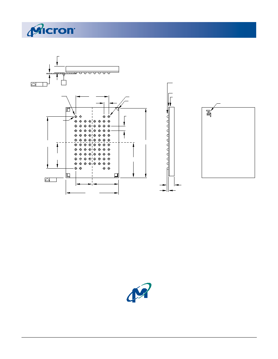
Figure 5: 88-Ball FBGA
NOTE:
1. All dimensions in millimeters.
2. Package width and length do not include mold protrusion; allowable mold protrusion is 0.27mm per side.
Data Sheet Designation
Advance:
This data sheet contains initial descriptions of products still under development.
For additional documentation concerning Flash and CellularRAM features, functional descriptions, program-
ming, and timing, please refer to the MT28F644W18 data sheet at
www.micron.com/flash
and the
MT45W2MW16FPA and MT45W4MW16FPA data sheets at
http://www.micron.com/cellularram
.
BALL A1 ID
BALL A1 ID
BALL A1
BALL A8
MOLD COMPOUND: EPOXY NOVOLAC
SUBSTRATE: PLASTIC LAMINATE
1.40 MAX
0.25 ±0.05
SOLDER BALL MATERIAL:
62% Sn, 36% Pb, 2% Ag
SOLDER BALL PAD: ÿ 0.30mm SOLDER MASK DEFINED
5.60
9.00 ±0.10
2.80 ±0.05
4.50 ±0.05
8.80
4.40 ±0.05
6.00 ±0.05
12.00 ±0.10
88X 0.35
ÿ
SOLDER BALL DIAMETER
REFERS TO POST REFLOW
CONDITION. THE
PRE-REFLOW DIAMETER
IS ÿ 0.35
C
L
C
L
SEATING PLANE
1.025 ±0.075
0.10 C
C
0.80
TYP
0.80
TYP
0.10
(4X)

256Mb MULTIBANK BURST FLASH
32Mb/64Mb ASYNC/PAGE CellularRAM COMBO
ADVANCE
09005aef80bcd58d
Micron Technology, Inc., reserves the right to change products or specifications without notice.
MT28C256564W18S_A.fm - Rev. A, Pub 6/03 EN
21
©2003 Micron Technology. Inc.
Revision History
∑ Original document, Rev. A . . . . . . . . . . . . . . . . . . . . . . . . . . . . . . . . . . . . . . . . . . . . . . . . . . . . . . . . . . . . . . . . . . . . . . . . . . 6/03