Document Outline
- Features/Options
- Ball Assignment, 67-Ball FBGA (Top View)
- General Description
- Architecture and Memory Organization
- Device Marking
- Table 1, Cross Reference for Abbreviated Device Marks
- Part Numbering Information
- Figure 1, Part Number Chart
- Table 2, Valid Part Number Combinations
- Block Diagram
- Flash Functional Block Diagram
- Ball Descriptions
- Ball Descriptions (continued)
- Truth Table - Flash
- Truth Table - SRAM
- Figure 2, Bottom Boot Block Device
- Figure 3, Top Boot Block Device
- Flash Memory Operating Modes
- Command State Machine
- Operations
- Command Definition
- Status Register
- Table 3, Command State Machine Codes For Device Mode Selection
- Command State Machine Operations
- Table 4, Command Definitions
- Table 5, Command Descriptions
- Table 5, Command Descriptions (conrinued)
- CLEAR STATUS REGISTER
- READ Operations
- Read Array
- Read Chip Protection Identification Data
- Read Query
- Read Status Register
- Table 6, Command State Machine Transition Table
- Table 6, Command State Machine Transition Table (continued)
- Table 6, Command State Machine Transition Table (continued)
- Table 6, Command State Machine Transition Table (continued)
- Table 6, Command State Machine Transition Table (continued)
- Table 7, Bus Operations
- Programming Operations
- PROGRAM SETUP Command
- Accelerated Programming Algorithm
- ERASE Operations
- Table 8, Status Register Bit Definition
- Figure 4, Automated Word Programming Flowchart
- Figure 5, PROGRAM SUSPEND/ PROGRAM RESUME Flowchart
- Figure 6, Accelerated Program Algorithm Flowchart
- Figure 7, BLOCK ERASE Flowchart
- Figure 8, ERASE SUSPEND/ERASE RESUME Flowchart
- Figure 9, CHECK BLOCK ERASE Flowchart
- READ-While-WRITE/ERASE Concurrency
- Figure 10, READ-While-WRITE Concurrency
- Block Locking
- Locked State
- Unlocked State
- Table 9, Block Locking State Transition
- Locked Down State
- Reading a Block's Lock Status
- Locking Operations During ERASE SUSPEND
- Status Register Error Checking
- Chip Protection Register
- Reading the Chip Protection Register
- Figure 12, Protection Register Memory Map
- Table 10, Chip Configuration Addressing
- Page Read Mode
- Asynchronous READ Cycle
- Standby Mode
- Automatic Power Save (APS) Mode
- Deep Power-Down Mode
- F_VPP/F_VCC Program and Erase Voltages
- Table 11, F_VPP Ranges (V)
- Device Reset
- Power-Up Sequence
- Flash Electrical Specifications
- Flash Timing Diagrams
- Two-Cycle PROGRAMMING/ERASE Operation
- Single Asynchronous READ Operation
- Single Asynchronous Page Mode READ Operation
- Reset Operation
- Table 12, CFI
- Table 12, CFI (continued)
- Absolute Maximum Ratings
- Recommended Operating Conditions
- Figure 13, AC Input/Output Reference Waveform
- Figure 14, Output Load Circuit
- Combined DC Charactersitics
- Combined DC Charactersitics (continued)
- Capacitance
- Flash READ Cycle Timing Requirements
- Flash WRITE Cycle Timing Requirements
- Flash ERASE and PROGRAM Cycle Timing Requirements
- SRAM Operating Modes
- SRAM Read Array
- SRAM Write Array
- SRAM Functional Block Diagram
- Timing Test Conditions
- SRAM READ Cycle Timing
- SRAM WRITE Cycle Timing
- SRAM Timing Diagrams
- READ Cycle 1
- READ Cycle 2
- WRITE Cycle
- WRITE Cycle 2
- 67-Ball FBGA Package Drawing

1
4 Meg x 16 Asynchronous/Page Flash 512K x 16 SRAM Combo Memory
©2002, Micron Technology, Inc.
MT28C6428P20_3.p65 ≠ Rev. 3, Pub. 7/02
4 MEG x 16 ASYNCHRONOUS/PAGE FLASH
512K x 16 SRAM COMBO MEMORY
ADVANCE
PRODUCTS AND SPECIFICATIONS DISCUSSED HEREIN ARE FOR EVALUATION AND REFERENCE PURPOSES ONLY AND ARE
SUBJECT TO CHANGE BY MICRON WITHOUT NOTICE. PRODUCTS ARE ONLY WARRANTED BY MICRON TO MEET MICRON'S
PRODUCTION DATA SHEET SPECIFICATIONS.
FLASH AND SRAM
COMBO MEMORY
MT28C6428P20
MT28C6428P18
Low Voltage, Extended Temperature
0.18µm Process Technology
FEATURES
∑ Flexible dual-bank architecture
∑ Support for true concurrent operations with no
latency:
Read bank b during program bank a and vice versa
Read bank b during erase bank a and vice versa
∑ Organization: 4,096K x 16 (Flash)
512K x 16 (SRAM)
∑ Basic configuration:
Flash
Bank a (16Mb Flash for data storage)
≠ Eight 4K-word parameter blocks
≠ Thirty-one 32K-word blocks
Bank b (48Mb Flash for program storage)
≠ Ninety-six 32K-word main blocks
SRAM
8Mb SRAM for data storage
≠ 512K-words
∑ F_V
CC
, V
CC
Q, F_V
PP
, S_V
CC
voltages
MT28C6428P20
1.80V (MIN)/2.20V (MAX) F_V
CC
read voltage
1.80V (MIN)/2.20V (MAX) S_V
CC
read voltage
1.80V (MIN)/2.20V (MAX) V
CC
Q
MT28C6428P18
1.70V (MIN)/1.90V (MAX) F_V
CC
read voltage
1.70V (MIN)/1.90V (MAX) S_V
CC
read voltage
1.70V (MIN)/1.90V (MAX) V
CC
Q
MT28C6428P20/P18
1.80V (TYP) F_V
PP
(in-system PROGRAM/ERASE)
1.0V (MIN) S_V
CC
(SRAM data retention)
12V ±5% (HV) F_V
PP
(in-house programming and
accelerated programming algorithm [APA]
activation)
∑ Asynchronous access time
Flash access time: 80ns @ 1.80V F_V
CC
SRAM access time: 80ns @ 1.80V S_V
CC
∑ Page Mode read access
Interpage read access: 80ns @ 1.80V F_V
CC
Intrapage read access: 30ns @ 1.80V F_V
CC
∑ Low power consumption
∑ Enhanced suspend options
ERASE-SUSPEND-to-READ within same bank
PROGRAM-SUSPEND-to-READ within same bank
ERASE-SUSPEND-to-PROGRAM within same bank
∑ Read/Write SRAM during program/erase of Flash
∑ Dual 64-bit chip protection registers for security
purposes
∑ PROGRAM/ERASE cycles
100,000 WRITE/ERASE cycles per block
∑ Cross-compatible command set support
Extended command set
Common flash interface (CFI) compliant
OPTIONS
MARKING
∑ Timing
80ns
-80
85ns
-85
∑ Boot Block Configuration
Top
T
Bottom
B
∑ Operating Voltage Range
F_V
CC
= 1.70V≠1.90V
18
F_V
CC
= 1.80V≠2.20V
20
∑ Operating Temperature Range
Commercial (0
o
C to +70
o
C)
None
Extended (-40
o
C to +85
o
C)
ET
∑ Package
67-ball FBGA (8 x 8 grid)
FM
Part Number Example:
MT28C6428P20FM-80 BET
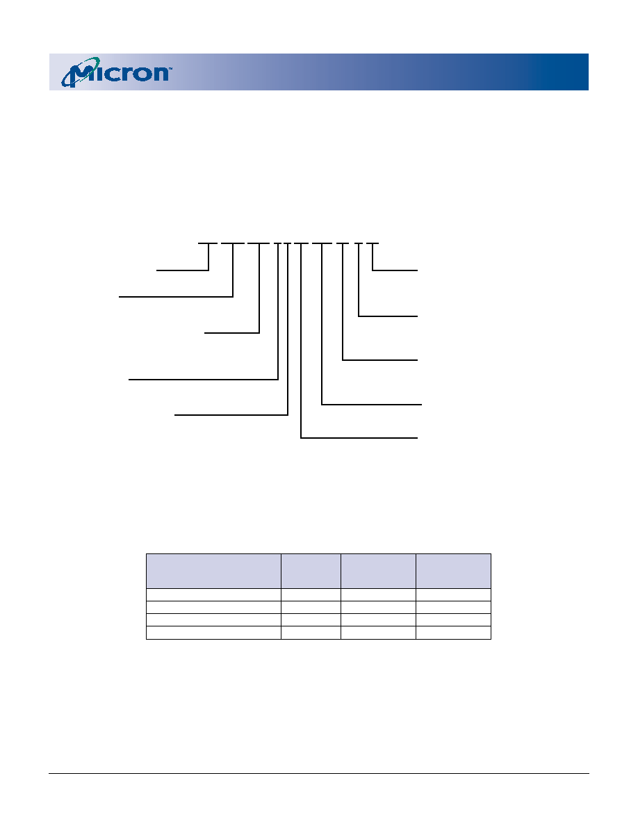
BALL ASSIGNMENT
67-Ball FBGA (Top View)
A
B
C
D
E
F
G
H
1 2 3 4 5 6 7 8 9 10 11
12
Top View
(Ball Down)
NC
NC
A14
A9
DQ11
A6
A0
A15
A10
A21
A19
S_OE#
A7
A4
A20
A16
F_WE#
VSS
F_WP#
S_LB#
A18
F_VCC
A12
S_WE#
DQ6
S_CE2
DQ10
DQ8
A2
F_VSS
F_VSS
DQ14
DQ4
S_VCC
DQ2
DQ0
A1
F_OE#
VccQ
DQ7
DQ5
F_VCC
DQ3
DQ1
S_CE1#
NC
NC
NC
NC
NC
A13
DQ15
DQ13
DQ12
DQ9
A3
F_CE#
NC
NC
A11
A8
NC
F_RP#
F_VPP
S_UB#
A17
A5

2
4 Meg x 16 Asynchronous/Page Flash 512K x 16 SRAM Combo Memory
Micron Technology, Inc., reserves the right to change products or specifications without notice.
MT28C6428P20_3.p65 ≠ Rev. 3, Pub. 7/02
©2002, Micron Technology, Inc.
4 MEG x 16 ASYNCHRONOUS/PAGE FLASH
512K x 16 SRAM COMBO MEMORY
ADVANCE
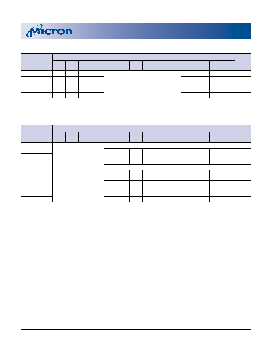
Table 1
Cross Reference for Abbreviated Device Marks
PRODUCT
SAMPLE
MECHANICAL
PART NUMBER
MARKING
MARKING
SAMPLE MARKING
MT28C6428P20FM-80 BET
FW454
FX454
FY454
MT28C6428P20FM-80 TET
FW453
FX453
FY453
MT28C6428P18FM-85 BET
FW455
FX455
FY455
MT28C6428P18FM-85 TET
FW452
FX452
FY452
GENERAL DESCRIPTION
The MT28C6428P20 and MT28C6428P18 combi-
nation Flash and SRAM memory devices provide a com-
pact, low-power solution for systems where PCB real
estate is at a premium. The dual-bank Flash devices
are high-performance, high-density, nonvolatile
memory with a revolutionary architecture that can sig-
nificantly improve system performance.
This new architecture features:
∑ A two-memory-bank configuration supporting
dual-bank operation;
∑ A high-performance bus interface providing a fast
page data transfer; and
∑ A conventional asynchronous bus interface.
The devices also provide soft protection for blocks
by configuring soft protection registers with dedicated
command sequences. For security purposes, dual 64-
bit chip protection registers are provided.
The embedded WORD WRITE and BLOCK ERASE
functions are fully automated by an on-chip write state
machine (WSM). The WSM simplifies these operations
and relieves the system processor of secondary tasks.
An on-chip status register, one for each bank, can be
used to monitor the WSM status to determine the
progress of a PROGRAM/ERASE command.
The erase/program suspend functionality allows
compatibility with existing EEPROM emulation soft-
ware packages.
The devices take advantage of a dedicated power
source for the Flash memory (F_V
CC
) and a dedicated
power source for the SRAM (S_V
CC
), both at 1.70V≠2.20V
for optimized power consumption and improved noise
immunity. A dedicated I/O power supply (V
CC
Q) is pro-
vided with an extended range (1.70V≠2.20V), to allow a
direct interface to most common logic controllers and
to ensure improved noise immunity. The separate
S_V
CC
pin for the SRAM provides data retention capa-
bility when required. The data retention S_V
CC
is speci-
fied as low as 1.0V. The MT28C6428P20 and
MT28C6428P18 devices support two F_V
PP
voltage
ranges, an in-circuit voltage of 0.9V≠2.2V and a produc-
tion compatibility voltage of 12V ±5%. The 12V ±5%
F_V
PP
2
is supported for a maximum of 100 cycles and 10
cumulative hours.
The MT28C6428P20 and MT28C6428P18 contain
an asynchronous 8Mb SRAM organized as 512K-words
by 16 bits. The devices are fabricated using an ad-
vanced CMOS process and high-speed/ultra-low-
power circuit technology, and then are packaged in a
67-ball FBGA package with 0.80mm pitch.
ARCHITECTURE AND MEMORY
ORGANIZATION
The Flash devices contain two separate banks of
memory (bank a and bank b) for simultaneous READ
and WRITE operations, which are available in the fol-
lowing bank segmentation configuration:
∑ Bank a comprises one-fourth of the memory and
contains 8 x 4K-word parameter blocks, while the
remainder of bank a is split into 31 x 32K-word
blocks.
∑ Bank b represents three-fourths of the memory, is
equally sectored, and contains 96 x 32K-word
blocks.
Figures 2 and 3 show the bottom and top memory
organizations.
DEVICE MARKING
Due to the size of the package, Micron's standard
part number is not printed on the top of each device.
Instead, an abbreviated device mark comprised of a
five-digit alphanumeric code is used. The abbreviated
device marks are cross referenced to Micron part num-
bers in Table 1.
3
4 Meg x 16 Asynchronous/Page Flash 512K x 16 SRAM Combo Memory
Micron Technology, Inc., reserves the right to change products or specifications without notice.
MT28C6428P20_3.p65 ≠ Rev. 3, Pub. 7/02
©2002, Micron Technology, Inc.
4 MEG x 16 ASYNCHRONOUS/PAGE FLASH
512K x 16 SRAM COMBO MEMORY
ADVANCE
PART NUMBERING INFORMATION
Micron's low-power devices are available with sev-
eral different combinations of features (see Figure 1).
Table 2
Valid Part Number Combinations
1
BOOT BLOCK
OPERATING
ACCESS
STARTING
TEMPERATURE
PART NUMBER
TIME (ns)
ADDRESS
RANGE
MT28C6428P20FM-80 BET
80
Bottom
-40
o
C to +85
o
C
MT28C6428P20FM-80 TET
80
Top
-40
o
C to +85
o
C
MT28C6428P18FM-85 BET
85
Bottom
-40
o
C to +85
o
C
MT28C6428P18FM-85 TET
85
Top
-40
o
C to +85
o
C
NOTE: 1. For part number combinations not listed in this table, please contact
your Micron representative.
Figure 1
Part Number Chart
Valid combinations of features and their correspond-
ing part numbers are listed in Table 2.
MT 28C 642 8 P 20 FM-80 T ET
Micron Technology
Flash Family
28C = Dual-Supply Flash/SRAM Combo
Density/Organization/Banks
642 = 64Mb (4,096K x 16)
bank a = 1/4; bank b = 3/4
SRAM Density
8 = 8Mb SRAM (512K x 16)
Access Time
-80 = 80ns
-85 = 85ns
Read Mode Operation
P = Asynchronous/Page Read
Package Code
FM = 67-ball FBGA (8 x 8 grid)
Operating Temperature Range
None = Commercial (0∫C to +70∫C)
ET = Extended (-40∫C to +85∫C)
Boot Block Starting Address
B = Bottom boot
T = Top boot
Operating Voltage Range
20 = 1.80V≠2.20V V
CC
18 = 1.70V≠1.90V
4
4 Meg x 16 Asynchronous/Page Flash 512K x 16 SRAM Combo Memory
Micron Technology, Inc., reserves the right to change products or specifications without notice.
MT28C6428P20_3.p65 ≠ Rev. 3, Pub. 7/02
©2002, Micron Technology, Inc.
4 MEG x 16 ASYNCHRONOUS/PAGE FLASH
512K x 16 SRAM COMBO MEMORY
ADVANCE
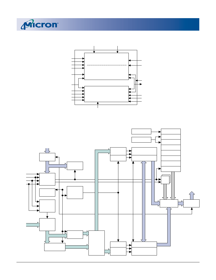
BLOCK DIAGRAM
F_V
PP
S_OE#
S_CE2
S_CE1#
S_WE#
DQ0
≠
DQ15
A19
≠
A20
A0
≠
A18
F_RP#
F_CE#
F_OE#
F_WE#
F_V
CC
F_WP#
F_V
SS
FLASH
SRAM
S_V
SS
S_UB#
S_LB#
4,096K x 16
512K x 16
Bank a
Bank b
S_V
CC
V
CC
Q
FLASH FUNCTIONAL BLOCK DIAGRAM
Address
Input
Buffer
X DEC
Y/Z DEC
Data Input
Buffer
Output
Multiplexer
Address
CNT/WSM
Output
Buffer
Status
Reg.
WSM
Program/
Erase
Pump Voltage
Generators
Address Latch
DQ0-DQ15
DQ0≠DQ15
CSM
F_RST#
F_CE#
X DEC
Y/Z DEC
F_WE#
F_OE#
I/O Logic
A0≠A21
Address
Multiplexer
Bank 2 Blocks
Y/Z Gating/Sensing
Data
Register
Bank 1 Blocks
Y/Z Gating/Sensing
ID Reg.
RCR
Block Lock
Device ID
Manufacturer's ID
OTP
Query
PR Lock
Query/OTP
PR Lock
5
4 Meg x 16 Asynchronous/Page Flash 512K x 16 SRAM Combo Memory
Micron Technology, Inc., reserves the right to change products or specifications without notice.
MT28C6428P20_3.p65 ≠ Rev. 3, Pub. 7/02
©2002, Micron Technology, Inc.
4 MEG x 16 ASYNCHRONOUS/PAGE FLASH
512K x 16 SRAM COMBO MEMORY
ADVANCE
BALL DESCRIPTIONS
67-BALL FBGA
NUMBERS
SYMBOL
TYPE
DESCRIPTION
H6, G9, G8, G7,
A0≠A21
Input
Address Inputs: Inputs for the addresses during READ and WRITE
H5, H4, G6, G5,
operations. Addresses are internally latched during READ and WRITE
B4, B6, B5, A4,
cycles. Flash: A0≠A21; SRAM: A0≠A18.
A8, A7, A6, A5,
B3, G4, G3, E5,
A3, C5
H7
F_CE#
Input
Flash Chip Enable: Activates the device when LOW. When CE# is HIGH,
the device is disabled and goes into standby power mode.
H9
F_OE#
Input
Flash Output Enable: Enables Flash output buffers when LOW. When
F_OE# is HIGH, the output buffers are disabled.
C3
F_WE#
Input
Flash Write Enable: Determines if a given cycle is a Flash WRITE cycle.
F_WE# is active LOW.
D4
F_RP#
Input
Reset. When F_RP# is a logic LOW, the device is in reset, which drives
the outputs to High-Z and resets the WSM. When F_RP# is a logic HIGH,
the device is in standard operation. When F_RP# transitions from logic
LOW to logic HIGH, the device resets all blocks to locked and defaults to
the read array mode.
E3
F_WP#
Input
Flash Write Protect. Controls the lock down function of the flexible
locking feature.
G10
S_CE1#
Input
SRAM Chip Enable1: Activates the SRAM when it is LOW. HIGH level
deselects the SRAM and reduces the power consumption to standby
levels.
D8
S_CE2
Input
SRAM Chip Enable2: Activates the SRAM when it is HIGH. LOW level
deselects the SRAM and reduces the power consumption to standby
levels.
F5
S_OE#
Input
SRAM Output Enable: Enables SRAM output buffers when LOW. When
S_OE# is HIGH, the output buffers are disabled.
B8
S_WE#
Input
SRAM Write Enable: Determines if a given cycle is an SRAM WRITE cycle.
S_WE# is active LOW.
F3
S_LB#
Input
SRAM Lower Byte: When LOW, it selects the SRAM address lower byte
(DQ0≠DQ7).
F4
S_UB#
Input
SRAM Upper Byte: When LOW, it selects the SRAM address upper byte
(DQ8≠DQ15).
F9, F10, E9,
DQ0≠DQ15
Input/
Data Inputs/Outputs: Input array data on the second CE# and WE#
E10, C9, C10,
Output
cycle during PROGRAM command. Input commands to the command
C8, B10, F8,
user interface when CE# and WE# are active. Output data when CE#
F7, E8, E6, D7,
and OE# are active.
C7, B9, B7
(continued on next page)
6
4 Meg x 16 Asynchronous/Page Flash 512K x 16 SRAM Combo Memory
Micron Technology, Inc., reserves the right to change products or specifications without notice.
MT28C6428P20_3.p65 ≠ Rev. 3, Pub. 7/02
©2002, Micron Technology, Inc.
4 MEG x 16 ASYNCHRONOUS/PAGE FLASH
512K x 16 SRAM COMBO MEMORY
ADVANCE
BALL DESCRIPTIONS (continued)
67-BALL FBGA
NUMBERS
SYMBOL
TYPE
DESCRIPTION
E4
F_V
PP
Input/
Flash Program/Erase Power Supply: [0.9V≠2.2V or 11.4V≠12.6V].
Supply
Operates as input at logic levels to control complete device protection.
Provides backward compatibility for factory programming when driven
to 11.4V≠12.6V. A lower F_V
PP
voltage range (0.0V≠2.2V) is available.
Contact factory for more information.
D10, H3
F_V
CC
Supply
Flash Power Supply: [1.70V≠1.90V or 1.80V≠2.20V]. Supplies power for
device operation.
A9, H8
F_V
SS
Supply
Flash Specific Ground: Do not float any ground ball.
D9
S_V
CC
Supply
SRAM Power Supply: [1.70V≠1.90V or 1.80V≠2.20V]. Supplies power for
device operation.
D3
S_V
SS
Supply
SRAM Specific Ground: Do not float any ground ball.
A10
V
CC
Q
Supply
I/O Power Supply: [1.70≠1.90V or 1.80V≠2.20V].
A1, A2, A11,
NC
≠
No Connect: Lead is not internally connected; it may be driven or
A12, C4, H1,
floated.
H2, H10, H11,
H12
C6, D5, D6,
≠
≠
Contact balls not mounted; corresponding position on PCB can be used
E7, F6
to reduce routing complexity.
7
4 Meg x 16 Asynchronous/Page Flash 512K x 16 SRAM Combo Memory
Micron Technology, Inc., reserves the right to change products or specifications without notice.
MT28C6428P20_3.p65 ≠ Rev. 3, Pub. 7/02
©2002, Micron Technology, Inc.
4 MEG x 16 ASYNCHRONOUS/PAGE FLASH
512K x 16 SRAM COMBO MEMORY
ADVANCE
NOTE: 1. Two devices may not drive the memory bus at the same time.
2. Allowable Flash read modes include read array, read query, read configuration, and read status.
3. Outputs are dependent on a separate device controlling bus outputs.
4. Modes of the Flash and SRAM can be interleaved so that while one is disabled, the other controls outputs.
5. SRAM is enabled and/or disabled with the logical function: S_CE1# or S_CE2.
6. Simultaneous operations can exist, as long as the operations are interleaved such that only one device attempts to
control the bus outputs at a time.
7. Data output on lower byte only; upper byte High-Z.
8. Data output on upper byte only; lower byte High-Z.
9. Data input on lower byte only.
10. Data input on upper byte only.
TRUTH TABLE ≠ FLASH
FLASH SIGNALS
SRAM SIGNALS
MEMORY OUPUT
MODES
F_RP# F_CE# F_OE# F_WE# S_CE1# S_CE2 S_OE# S_WE# S_UB# S_LB#
MEMORY
DQ0≠DQ15
NOTES
BUS CONTROL
Read
H
L
L
H
SRAM must be High-Z
Flash
D
OUT
1, 2, 3
Write
H
L
H
L
Flash
D
IN
1
Standby
H
H
X
X
Other
High-Z
4
Output Disable
H
L
H
H
SRAM any mode allowable
Other
High-Z
4, 5
Reset
L
X
X
X
Other
High-Z
4, 6
TRUTH TABLE ≠ SRAM
FLASH SIGNALS
SRAM SIGNALS
MEMORY OUPUT
MODES
F_RP# F_CE# F_OE# F_WE# S_CE1# S_CE2 S_OE# S_WE# S_UB# S_LB#
MEMORY
DQ0≠DQ15
NOTES
BUS CONTROL
Read
DQ0≠DQ15
L
H
L
H
L
L
SRAM
D
OUT
1, 3
DQ0≠DQ7
L
H
L
H
H
L
SRAM
D
OUT
LB
7
DQ8≠DQ15
Flash must be High-Z
L
H
L
H
L
H
SRAM
D
OUT
UB
8
Write
DQ0≠DQ15
L
H
H
L
L
L
SRAM
D
IN
1, 3
DQ0≠DQ7
L
H
H
L
H
L
SRAM
D
IN
LB
9
DQ8≠DQ15
L
H
H
L
L
H
SRAM
D
IN
UB
10
Standby
H
X
X
X
X
X
Other
High-Z
4
Flash any mode allowable
X
L
X
X
X
X
Other
High-Z
4
Output Disable
L
H
X
X
X
X
Other
High-Z
4
FLASH
8
4 Meg x 16 Asynchronous/Page Flash 512K x 16 SRAM Combo Memory
Micron Technology, Inc., reserves the right to change products or specifications without notice.
MT28C6428P20_3.p65 ≠ Rev. 3, Pub. 7/02
©2002, Micron Technology, Inc.
4 MEG x 16 ASYNCHRONOUS/PAGE FLASH
512K x 16 SRAM COMBO MEMORY
ADVANCE
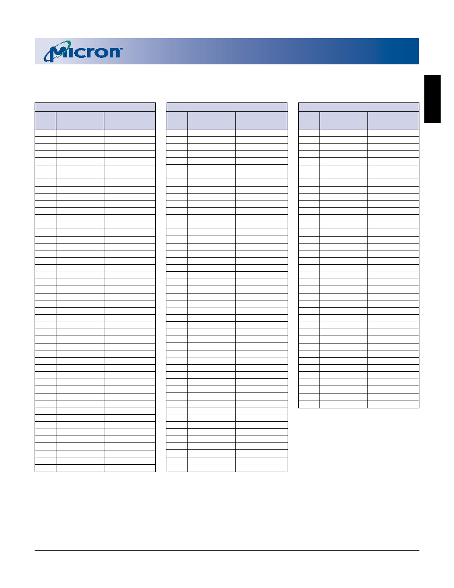
Figure 2
Bottom Boot Block Device
Bank a = 16Mb
Block
Block Size
Address Range
(K-bytes/
(x16)
K-words)
38
64/32
0F8000h≠0FFFFFh
37
64/32
0F0000h≠0F7FFFh
36
64/32
0E8000h≠0EFFFFh
35
64/32
0E0000h≠0E7FFFh
34
64/32
0D8000h≠0DFFFFh
33
64/32
0D0000h≠0D7FFFh
32
64/32
0C8000h≠0CFFFFh
31
64/32
0C0000h≠0C7FFFh
30
64/32
0B8000h≠0BFFFFh
29
64/32
0B0000h≠0B7FFFh
28
64/32
0A8000h≠0AFFFFh
27
64/32
0A0000h≠0A7FFFh
26
64/32
098000h≠097FFFh
25
64/32
090000h≠097FFFh
24
64/32
088000h≠087FFFh
23
64/32
080000h≠087FFFh
22
64/32
078000h≠07FFFFh
21
64/32
070000h≠077FFFh
20
64/32
068000h≠067FFFh
19
64/32
060000h≠067FFFh
18
64/32
058000h≠05FFFFh
17
64/32
050000h≠057FFFh
16
64/32
048000h≠04FFFFh
15
64/32
040000h≠047FFFh
14
64/32
038000h≠03FFFFh
13
64/32
030000h≠037FFFh
12
64/32
028000h≠02FFFFh
11
64/32
020000h≠027FFFh
10
64/32
018000h≠01FFFFh
9
64/32
010000h≠017FFFh
8
64/32
008000h≠00FFFFh
7
8/4
007000h≠007FFFh
6
8/4
006000h≠006FFFh
5
8/4
005000h≠005FFFh
4
8/4
004000h≠004FFFh
3
8/4
003000h≠003FFFh
2
8/4
002000h≠002FFFh
1
8/4
001000h≠001FFFh
0
8/4
000000h≠000FFFh
Bank b = 48Mb
Block
Block Size
Address Range
(K-bytes/
(x16)
K-words)
134
64/32
3F8000h≠3FFFFFh
133
64/32
3F0000h≠3F7FFFh
132
64/32
3E8000h≠3EFFFFh
131
64/32
3E0000h≠3E7FFFh
130
64/32
3D8000h≠3DFFFFh
129
64/32
3D0000h≠3D7FFFh
128
64/32
3C8000h≠3CFFFFh
127
64/32
3C0000h≠3C7FFFh
126
64/32
3B8000h≠3BFFFFh
125
64/32
3B0000h≠3B7FFFh
124
64/32
3A8000h≠3AFFFFh
123
64/32
3A0000h≠3A7FFFh
122
64/32
398000h≠39FFFFh
121
64/32
390000h≠397FFFh
120
64/32
388000h≠38FFFFh
119
64/32
380000h≠387FFFh
118
64/32
378000h≠37FFFFh
117
64/32
370000h≠377FFFh
116
64/32
368000h≠36FFFFh
115
64/32
360000h≠367FFFh
114
64/32
358000h≠35FFFFh
113
64/32
350000h≠357FFFh
112
64/32
348000h≠34FFFFh
111
64/32
340000h≠347FFFh
110
64/32
338000h≠33FFFFh
109
64/32
330000h≠337FFFh
108
64/32
328000h≠32FFFFh
107
64/32
320000h≠327FFFh
106
64/32
318000h≠31FFFFh
105
64/32
310000h≠317FFFh
104
64/32
308000h≠30FFFFh
103
64/32
300000h≠307FFFh
102
64/32
2F8000h≠2FFFFFh
101
64/32
2F0000h≠2F7FFFh
100
64/32
2E8000h≠2EFFFFh
99
64/32
2E0000h≠2E7FFFh
98
64/32
2D8000h≠2DFFFFh
97
64/32
2D0000h≠2D7FFFh
96
64/32
2C8000h≠2CFFFFh
95
64/32
2C0000h≠2C7FFFh
94
64/32
2B8000h≠2BFFFFh
93
64/32
2B0000h≠2B7FFFh
92
64/32
2A8000h≠2AFFFFh
91
64/32
2A0000h≠2A7FFFh
90
64/32
298000h≠29FFFFh
89
64/32
290000h≠297FFFh
88
64/32
288000h≠28FFFFh
87
64/32
280000h≠287FFFh
Bank b = 48Mb
Block
Block Size
Address Range
(K-bytes/
(x16)
K-words)
86
64/32
278000H≠27FFFFh
85
64/32
270000h≠277FFFh
84
64/32
268000h≠26FFFFh
83
64/32
260000h≠267FFFh
82
64/32
258000h≠25FFFFh
81
64/32
250000h≠257FFFh
80
64/32
248000h≠24FFFFh
79
64/32
240000h≠247FFFh
78
64/32
238000h≠23FFFFh
77
64/32
230000h≠237FFFh
76
64/32
228000h≠22FFFFh
75
64/32
220000h≠227FFFh
74
64/32
218000h≠21FFFFh
73
64/32
210000h≠217FFFh
72
64/32
208000h≠20FFFFh
71
64/32
200000h≠207FFFh
70
64/32
1F8000h≠1FFFFFh
69
64/32
1F0000h≠1F7FFFh
68
64/32
1E8000h≠1EFFFFh
67
64/32
1E0000h≠1E7FFFh
66
64/32
1D8000h≠1DFFFFh
65
64/32
1D0000h≠1D7FFFh
64
64/32
1C8000h≠1CFFFFh
63
64/32
1C0000h≠1C7FFFh
62
64/32
1B8000h≠1BFFFFh
61
64/32
1B0000h≠1B7FFFh
60
64/32
1A8000h≠1AFFFFh
59
64/32
1A0000h≠1A7FFFh
58
64/32
198000h≠19FFFFh
57
64/32
190000h≠197FFFh
56
64/32
188000h≠18FFFFh
55
64/32
180000h≠187FFFh
54
64/32
178000h≠17FFFFh
53
64/32
170000h≠177FFFh
52
64/32
168000h≠16FFFFh
51
64/32
160000h≠167FFFh
50
64/32
158000h≠15FFFFh
49
64/32
150000h≠157FFFh
48
64/32
148000h≠14FFFFh
47
64/32
140000h≠147FFFh
46
64/32
138000h≠13FFFFh
45
64/32
130000h≠137FFFh
44
64/32
128000h≠12FFFFh
43
64/32
120000h≠127FFFh
42
64/32
118000h≠11FFFFh
41
64/32
110000h≠117FFFh
40
64/32
108000h≠10FFFFh
39
64/32
100000h≠107FFFh
FLASH
9
4 Meg x 16 Asynchronous/Page Flash 512K x 16 SRAM Combo Memory
Micron Technology, Inc., reserves the right to change products or specifications without notice.
MT28C6428P20_3.p65 ≠ Rev. 3, Pub. 7/02
©2002, Micron Technology, Inc.
4 MEG x 16 ASYNCHRONOUS/PAGE FLASH
512K x 16 SRAM COMBO MEMORY
ADVANCE
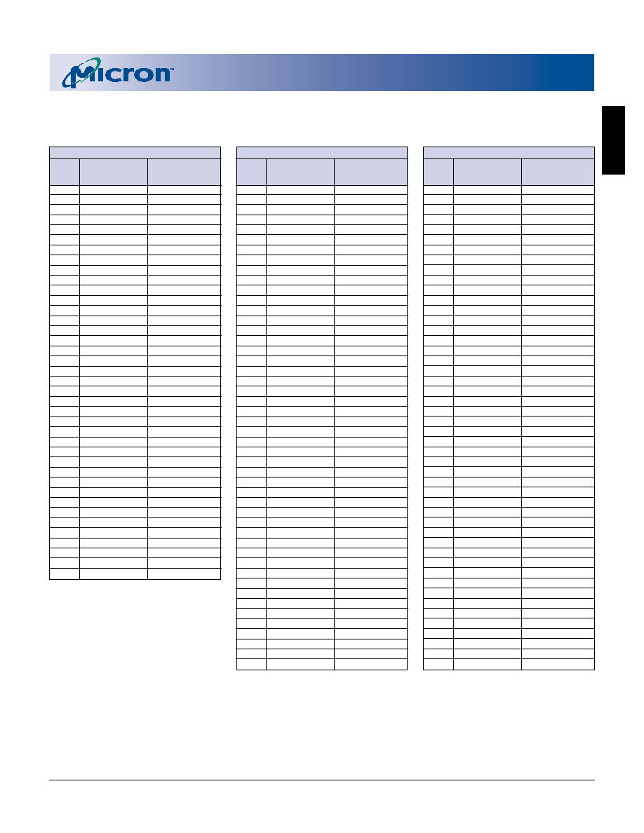
Figure 3
Top Boot Block Device
Bank a = 16Mb
Block
Block Size
Address Range
(K-bytes/
(x16)
K-words)
134
8/4
3FF000h≠3FFFFFh
133
8/4
3FE000h≠3FEFFFh
132
8/4
3FD000h≠3FDFFFh
131
8/4
3FC000h≠3FCFFFh
130
8/4
3FB000h≠3FBFFFh
129
8/4
3FA000h≠3FAFFFh
128
8/4
3F9000h≠3F9FFFh
127
8/4
3F8000h≠3F8FFFh
126
64/32
3F0000h≠3F7FFFh
125
64/32
3E8000h≠3EFFFFh
124
64/32
3E0000h≠3E7FFFh
123
64/32
3D8000h≠3DFFFFh
122
64/32
3D0000h≠3D7FFFh
121
64/32
3C8000h≠3CFFFFh
120
64/32
3C0000h≠3C7FFFh
119
64/32
3B8000h≠3BFFFFh
118
64/32
3B0000h≠3B7FFFh
117
64/32
3A8000h≠3AFFFFh
116
64/32
3A0000h≠3A7FFFh
115
64/32
398000h≠39FFFFh
114
64/32
390000h≠397FFFh
113
64/32
388000h≠38FFFFh
112
64/32
380000h≠387FFFh
111
64/32
378000h≠37FFFFh
110
64/32
370000h≠377FFFh
109
64/32
368000h≠36FFFFh
108
64/32
360000h≠367FFFh
107
64/32
358000h≠35FFFFh
106
64/32
350000h≠357FFFh
105
64/32
348000h≠34FFFFh
104
64/32
340000h≠347FFFh
103
64/32
338000h≠33FFFFh
102
64/32
330000h≠337FFFh
101
64/32
328000h≠32FFFFh
100
64/32
320000h≠327FFFh
99
64/32
318000h≠31FFFFh
98
64/32
310000h≠317FFFh
97
64/32
308000h≠30FFFFh
96
64/32
300000h≠307FFFh
Bank b = 48Mb
Block
Block Size
Address Range
(K-bytes/
(x16)
K-words)
95
64/32
2F8000h≠2FFFFFh
94
64/32
2F0000h≠2F7FFFh
93
64/32
2E8000h≠2EFFFFh
92
64/32
2E0000h≠2E7FFFh
91
64/32
2D8000h≠2DFFFFh
90
64/32
2D0000h≠2D7FFFh
89
64/32
2C8000h≠2CFFFFh
88
64/32
2C0000h≠2C7FFFh
87
64/32
2B8000h≠2BFFFFh
86
64/32
2B0000h≠2B7FFFh
85
64/32
2A8000h≠2AFFFFh
84
64/32
2A0000h≠2A7FFFh
83
64/32
298000h≠29FFFFh
82
64/32
290000h≠297FFFh
81
64/32
288000h≠28FFFFh
80
64/32
280000h≠287FFFh
79
64/32
278000h≠27FFFFh
78
64/32
270000h≠277FFFh
77
64/32
268000h≠26FFFFh
76
64/32
260000h≠267FFFh
75
64/32
258000h≠25FFFFh
74
64/32
250000h≠257FFFh
73
64/32
248000h≠24FFFFh
72
64/32
240000h≠247FFFh
71
64/32
238000h≠23FFFFh
70
64/32
230000h≠237FFFh
69
64/32
228000h≠22FFFFh
68
64/32
220000h≠227FFFh
67
64/32
218000h≠21FFFFh
66
64/32
210000h≠217FFFh
65
64/32
208000h≠20FFFFh
64
64/32
200000h≠207FFFh
63
64/32
1F8000h≠1FFFFFh
62
64/32
1F0000h≠1F7FFFh
61
64/32
1E8000h≠1EFFFFh
60
64/32
1E0000h≠1E7FFFh
59
64/32
1D8000h≠1DFFFFh
58
64/32
1D0000h≠1D7FFFh
57
64/32
1C8000h≠1CFFFFh
56
64/32
1C0000h≠1C7FFFh
55
64/32
1B8000h≠1BFFFFh
54
64/32
1B0000h≠1B7FFFh
53
64/32
1A8000h≠1AFFFFh
52
64/32
1A0000h≠1A7FFFh
51
64/32
198000h≠19FFFFh
50
64/32
190000h≠197FFFh
49
64/32
188000h≠18FFFFh
48
64/32
180000h≠187FFFh
Bank b = 48Mb
Block
Block Size
Address Range
(K-bytes/
(x16)
K-words)
47
64/32
178000h≠17FFFFh
46
64/32
170000h≠177FFFh
45
64/32
168000h≠16FFFFh
44
64/32
160000h≠167FFFh
43
64/32
158000h≠15FFFFh
42
64/32
150000h≠157FFFh
41
64/32
148000h≠14FFFFh
40
64/32
140000h≠147FFFh
39
64/32
138000h≠13FFFFh
38
64/32
130000h≠137FFFh
37
64/32
128000h≠12FFFFh
36
64/32
120000h≠127FFFh
35
64/32
118000h≠11FFFFh
34
64/32
110000h≠117FFFh
33
64/32
108000h≠10FFFFh
32
64/32
100000h≠107FFFh
31
64/32
0F8000h≠0FFFFFh
30
64/32
0F0000h≠0F7FFFh
29
64/32
0E8000h≠0EFFFFh
28
64/32
0E0000h≠0E7FFFh
27
64/32
0D8000h≠0DFFFFh
26
64/32
0D0000h≠0D7FFFh
25
64/32
0C8000h≠0CFFFFh
24
64/32
0C0000h≠0C7FFFh
23
64/32
0B8000h≠0BFFFFh
22
64/32
0B0000h≠0B7FFFh
21
64/32
0A8000h≠0AFFFFh
20
64/32
0A0000h≠0A7FFFh
19
64/32
098000h≠09FFFFh
18
64/32
090000h≠097FFFh
17
64/32
088000h≠08FFFFh
16
64/32
080000h≠087FFFh
15
64/32
078000h≠07FFFFh
14
64/32
070000h≠077FFFh
13
64/32
068000h≠06FFFFh
12
64/32
060000h≠067FFFh
11
64/32
058000h≠05FFFFh
10
64/32
050000h≠057FFFh
9
64/32
048000h≠04FFFFh
8
64/32
040000h≠047FFFh
7
64/32
038000h≠03FFFFh
6
64/32
030000h≠037FFFh
5
64/32
028000h≠02FFFFh
4
64/32
020000h≠027FFFh
3
64/32
018000h≠01FFFFh
2
64/32
010000h≠017FFFh
1
64/32
008000h≠00FFFFh
0
64/32
000000h≠007FFFh

FLASH
10
4 Meg x 16 Asynchronous/Page Flash 512K x 16 SRAM Combo Memory
Micron Technology, Inc., reserves the right to change products or specifications without notice.
MT28C6428P20_3.p65 ≠ Rev. 3, Pub. 7/02
©2002, Micron Technology, Inc.
4 MEG x 16 ASYNCHRONOUS/PAGE FLASH
512K x 16 SRAM COMBO MEMORY
ADVANCE
FLASH MEMORY OPERATING MODES
COMMAND STATE MACHINE
Commands are issued to the command state ma-
chine (CSM) using standard microprocessor write tim-
ings. The CSM acts as an interface between external
microprocessors and the internal write state machine
(WSM). The available commands are listed in Table 3,
their definitions are given in Table 4 and their descrip-
tions in Table 5. Program and erase algorithms are au-
tomated by the on-chip WSM. Table 7 shows the CSM
transition states.
Once a valid PROGRAM/ERASE command is en-
tered, the WSM executes the appropriate algorithm,
which generates the necessary timing signals to con-
trol the device internally. A command is valid only if the
exact sequence of WRITEs is completed. After the WSM
completes its task, the write state machine status
(WSMS) bit (SR7) (see Table 8) is set to a logic HIGH
level (V
IH
), allowing the CSM to respond to the full com-
mand set again.
OPERATIONS
Device operations are selected by entering a stan-
dard JEDEC 8-bit command code with conventional
microprocessor timings into an on-chip CSM through
I/Os DQ0≠DQ7. The number of bus cycles required to
activate a command is typically one or two. The first
operation is always a WRITE. Control signals F_CE#
and F_WE# must be at a logic LOW level (V
IL
), and F_OE#
and F_RP# must be at logic HIGH (V
IH
). The second
operation, when needed, can be a WRITE or a READ
depending upon the command. During a READ opera-
tion, control signals F_CE# and F_OE# must be at a
logic LOW level (V
IL
), and F_WE# and F_RP# must be at
logic HIGH (V
IH
).
Table 7 illustrates the bus operations for all the
modes: write, read, reset, standby, and output disable.
When the device is powered up, internal reset cir-
cuitry initializes the chip to a read array mode of opera-
tion. Changing the mode of operation requires that a
command code be entered into the CSM. For each one
of the two Flash memory partitions, an on-chip status
register is available. These two registers allow the moni-
toring of the progress of various operations that can
take place on a memory bank. One of the two status
registers is interrogated by entering a READ STATUS
REGISTER command onto the CSM (cycle 1), specify-
ing an address within the memory partition boundary,
and reading the register data on I/O pins DQ0≠DQ7
(cycle 2). Status register bits SR0-SR7 correspond to
DQ0≠DQ7 (see Table 8).
COMMAND DEFINITION
Once a specific command code has been entered,
the WSM executes an internal algorithm, generating
the necessary timing signals to program, erase, and
verify data. See Table 4 for the CSM command defini-
tions and data for each of the bus cycles.
STATUS REGISTER
The status register allows the user to determine
whether the state of a PROGRAM/ERASE operation is
pending or complete. The status register is monitored
by toggling F_OE# and F_CE# and reading the result-
ing status code on I/Os DQ0≠DQ7. The high-order I/Os
(DQ8≠DQ15) are set to 00h internally, so only the low-
order I/Os (DQ0≠DQ7) need to be interpreted. Address
lines select the status register pertinent to the selected
memory partition.
Table 3
Command State Machine Codes For
Device Mode Selection
COMMAND
DQ0≠DQ7
CODE ON DEVICE MODE
10h
Accelerated Programming Algorithm
(APA)
20h
Block erase setup
40h
Program setup
50h
Clear status register
60h
Protection configuration setup
60h
Enable/disable deep power-down
70h
Read status register
90h
Read protection configuration
register
98h
Read query
B0h
Program/erase suspend
C0h
Protection register program/lock
D0h
Program/erase resume ≠ erase
confirm
D1h
Check block erase confirm
FFh
Read array
FLASH
11
4 Meg x 16 Asynchronous/Page Flash 512K x 16 SRAM Combo Memory
Micron Technology, Inc., reserves the right to change products or specifications without notice.
MT28C6428P20_3.p65 ≠ Rev. 3, Pub. 7/02
©2002, Micron Technology, Inc.
4 MEG x 16 ASYNCHRONOUS/PAGE FLASH
512K x 16 SRAM COMBO MEMORY
ADVANCE
Register data is updated and latched on the falling
edge of F_OE# or F_CE#, whichever occurs last. The
latest falling edge of either of these two signals up-
dates the latch within a given READ cycle. Latching the
data prevents errors from occurring if the register input
changes during a status register read.
The status register provides the internal state of the
WSM to the external microprocessor. During periods
when the WSM is active, the status register can be polled
to determine the WSM status. Table 8 defines the sta-
tus register bits.
After monitoring the status register during a
PROGRAM/ERASE operation, the data appearing on
DQ0≠DQ7 remains as status register data until a new
command is issued to the CSM. To return the device to
other modes of operation, a new command must be
issued to the CSM.
COMMAND STATE MACHINE OPERATIONS
The CSM decodes instructions for the commands
listed in Table 3. The 8-bit command code is input to
the device on DQ0≠DQ7 (see Table 4 for command
definitions). During a PROGRAM or ERASE cycle, the
CSM informs the WSM that a PROGRAM or ERASE cycle
has been requested.
During a PROGRAM cycle, the WSM controls the
program sequences and the CSM responds to a PRO-
GRAM SUSPEND command only.
During an ERASE cycle, the CSM responds to an
ERASE SUSPEND command only. When the WSM has
completed its task, the WSMS bit (SR7) is set to a logic
HIGH level and the CSM responds to the full command
set. The CSM stays in the current command state until
the microprocessor issues another command.
The WSM successfully initiates an ERASE or PRO-
GRAM operation only when F_V
PP
is within its correct
voltage range.
Table 4
Command Definitions
FIRST BUS CYCLE
SECOND BUS CYCLE
COMMAND
OPERATION ADDRESS
1
DATA
OPERATION ADDRESS
1
DATA
1
READ ARRAY
WRITE
WA
FFh
READ PROTECTION CONFIGURATION REGISTER
WRITE
IA
90h
READ
IA
ID
READ STATUS REGISTER
WRITE
BA
70h
READ
X
SRD
CLEAR STATUS REGISTER
WRITE
BA
50h
READ QUERY
WRITE
QA
98h
READ
QA
QD
BLOCK ERASE SETUP
WRITE
BA
20h
WRITE
BA
D0h
PROGRAM SETUP
WRITE
WA
40h
WRITE
WA
WD
ACCELERATED PROGRAMMING ALGORITHM (APA)
WRITE
WA
10h
WRITE
WA
WD
PROGRAM/ERASE SUSPEND
WRITE
BA
B0h
PROGRAM/ERASE RESUME ≠ ERASE CONFIRM
WRITE
BA
D0h
LOCK BLOCK
WRITE
BA
60h
WRITE
BA
01h
UNLOCK BLOCK
WRITE
BA
60h
WRITE
BA
D0h
LOCK DOWN BLOCK
WRITE
BA
60h
WRITE
BA
2Fh
CHECK BLOCK ERASE
WRITE
BA
20h
WRITE
BA
D1h
PROTECTION REGISTER PROGRAM
WRITE
PA
C0h
WRITE
PA
PD
PROTECTION REGISTER LOCK
WRITE
LPA
C0h
WRITE
LPA
FFFDh
ENABLE/DISABLE DEEP POWER-DOWN
WRITE
DPW
60h
WRITE
DPW
03h
NOTE: 1. BA:
Address within the block
DPW: BBCFh = Disable deep power-down
BBDFh = Enable deep power-down
IA:
Identification code address
ID:
Identification code data
LPA: Lock protection register address
PA:
Protection register address
PD:
Data to be written at location PA
QA: Query code address
QD: Query code data
SRD: Data read from the status register
WA: Word address of memory location to be written, or read
WD: Data to be written at the location WA
X:
"Don't Care"
FLASH
12
4 Meg x 16 Asynchronous/Page Flash 512K x 16 SRAM Combo Memory
Micron Technology, Inc., reserves the right to change products or specifications without notice.
MT28C6428P20_3.p65 ≠ Rev. 3, Pub. 7/02
©2002, Micron Technology, Inc.
4 MEG x 16 ASYNCHRONOUS/PAGE FLASH
512K x 16 SRAM COMBO MEMORY
ADVANCE
Table 5
Command Descriptions
CODE DEVICE MODE
BUS CYCLE
DESCRIPTION
10h
APA
First
Prepares for an accelerated program operation.
20h
Erase Setup
First
Prepares the CSM for the ERASE command. If the next command is
not a CHECK BLOCK ERASE OR ERASE CONFIRM command, the
command will be ignored, and the device will go to read status
mode and wait for another command.
40h
Program Setup
First
A two-cycle command: The first cycle prepares for a PROGRAM
operation, the second cycle latches addresses and data and initiates
the WSM to execute the program algorithm. The Flash outputs status
register data on the falling edge of F_OE# or F_CE#, whichever
occurs first.
50h
Clear Status
First
The WSM can set the program status (SR4), and erase status (SR5) bits
Register
in the status register to "1," but it cannot clear them to "0." Issuing
this command clears those bits to "0."
60h
Protection
First
Prepares the CSM for changes to the block locking status. If the next
Configuration
command is not BLOCK UNLOCK, BLOCK LOCK or BLOCK LOCK
Setup
DOWN, the command will be ignored, and the device will go to read
status mode.
Set Read
First
Puts the device into the set read configuration mode so that it will be
Configuration
possible to set the option bits related to burst read mode.
Register
70h
Read Status
First
Places the device into read status register mode. Reading the device
Register
outputs the contents of the status register for the addressed bank.
The device automatically enters this mode for the addressed bank
after a PROGRAM or ERASE operation has been initiated.
90h
Read Protection
First
Puts the device into the read protection configuration mode so that
Configuration
reading the device outputs the manufacturer/device codes or block
lock status.
98h
Read Query
First
Puts the device into the read query mode so that reading the device
outputs common Flash interface information.
B0h
Program Suspend
First
Suspends the currently executing PROGRAM/ERASE/CHECK BLOCK
ERASE operation. The status register indicates when the operation
Erase Suspend
First
has been successfully suspended by setting either the program
suspend (SR2) or erase suspend (SR6) and the WSMS bit (SR7) to a
Check Block
First
"1" (ready). The WSM continues to idle in the suspend state,
Erase Suspend
regardless of the state of all input control pins except F_RP#, which
immediately shuts down the WSM and the remainder of the chip if
F_RP# is driven to V
IL
.
C0h
Program Device
First
Writes a specific code into the device protection register.
Protection Register
Lock Device
First
Locks the device protection register; data can no longer be changed.
Protection Register
(continued on the next page)
FLASH
13
4 Meg x 16 Asynchronous/Page Flash 512K x 16 SRAM Combo Memory
Micron Technology, Inc., reserves the right to change products or specifications without notice.
MT28C6428P20_3.p65 ≠ Rev. 3, Pub. 7/02
©2002, Micron Technology, Inc.
4 MEG x 16 ASYNCHRONOUS/PAGE FLASH
512K x 16 SRAM COMBO MEMORY
ADVANCE
Table 5
Command Descriptions (continued)
CODE DEVICE MODE
BUS CYCLE
DESCRIPTION
D0h
Erase Confirm
Second
If the previous command was an ERASE SETUP command, then the
CSM closes the address and data latches, and it begins erasing the
block indicated on the address pins. During programming/erase, the
device responds only to the READ STATUS REGISTER, PROGRAM
SUSPEND, or ERASE SUSPEND commands and outputs status register
data on the falling edge of F_OE# or F_CE#, whichever occurs last.
Program/Erase/
First
If a PROGRAM, ERASE or CHECK BLOCK ERASE operation was
Check Block Erase
previously suspended, this command resumes the operation.
Resume
FFh
Read Array
First
During the array mode, array data is output on the data bus.
01h
Lock Block
Second
If the previous command was PROTECTION CONFIGURATION SETUP,
the CSM latches the address and locks the block indicated on the
address bus.
2Fh
Lock Down
Second
If the previous command was PROTECTION CONFIGURATION SETUP,
the CSM latches the address and locks down the block indicated on
the address bus.
D0h
Unlock Block
Second
If the previous command was PROTECTION CONFIGURATION SETUP,
the CSM latches the address and unlocks the block indicated on the
address bus. If the block had been previously set to lock down, this
operation has no effect.
00h
Invalid/Reserved
Unassigned command that should not be used.
D1h
Check Block
Second
If the previous command was ERASE SETUP command, the CSM
Erase Confirm
closes the address latches and checks that the block is completely
erased.

FLASH
14
4 Meg x 16 Asynchronous/Page Flash 512K x 16 SRAM Combo Memory
Micron Technology, Inc., reserves the right to change products or specifications without notice.
MT28C6428P20_3.p65 ≠ Rev. 3, Pub. 7/02
©2002, Micron Technology, Inc.
4 MEG x 16 ASYNCHRONOUS/PAGE FLASH
512K x 16 SRAM COMBO MEMORY
ADVANCE
CLEAR STATUS REGISTER
The internal circuitry can set, but not clear, the block
lock status bit (SR1), the F_V
PP
status bit (SR3), the
program status bit (SR4), and the erase status bit (SR5)
of the status register. The CLEAR STATUS REGISTER
command (50h) allows the external microprocessor to
clear these status bits and synchronize to the internal
operations. When the status bits are cleared, the de-
vice returns to the read array mode.
READ OPERATIONS
The following READ operations are available: READ
ARRAY, READ PROTECTION CONFIGURATION REG-
ISTER, READ QUERY and READ STATUS REGISTER.
READ ARRAY
The array is read by entering the command code
FFh on DQ0≠DQ7. Control signals F_CE# and F_OE#
must be at a logic LOW level (V
IL
), and F_WE# and F_RP#
must be at a logic HIGH level (V
IH
) to read data from the
array. Data is available on DQ0≠DQ15. Any valid ad-
dress within any of the blocks selects that address and
allows data to be read from that address. Upon initial
power-up or device reset, the device defaults to the
read array mode.
READ CHIP PROTECTION IDENTIFICATION DATA
The chip identification mode outputs three types
of information: the manufacturer/device identifier, the
block locking status, and the protection register. Two
bus cycles are required for this operation: the chip iden-
tification data is read by entering the command code
90h on DQ0≠DQ7 to the bank containing address 00h
and the identification code address on the address
lines. Control signals F_CE# and F_OE# must be at a
logic LOW level (V
IL
), and F_WE# and F_RP# must be at
a logic HIGH level (V
IH
) to read data from the protection
configuration register. Data is available on DQ0≠DQ15.
After data is read from protection configuration regis-
ter, the READ ARRAY command, FFh, must be issued to
the bank containing address 00h prior to issuing other
commands. See Table 10 for further details.
READ QUERY
The read query mode outputs common flash inter-
face (CFI) data when the device is read (see Table 12).
Two bus cycles are required for this operation. It is
possible to access the query by writing the read query
command code 98h on DQ0≠DQ7 to the bank contain-
ing address 0h. Control signals F_CE# and F_OE# must
be at a logic LOW level (V
IL
), and F_WE# and F_RP#
must be at a logic HIGH level (V
IH
) to read data from the
query. The CFI data structure contains information
such as block size, density, command set, and electri-
cal specifications. To return to read array mode, write
the read array command code FFh on DQ0≠DQ7.
READ STATUS REGISTER
The status register is read by entering the command
code 70h on DQ0≠DQ7. Two bus cycles are required for
this operation: one to enter the command code and a
second to read the status register. In a READ cycle, the
address is latched and register data is updated on the
falling edge of F_OE# or F_CE#, whichever occurs last.
Register data is updated and latched on the falling
edge of F_OE# or F_CE#, whichever occurs last.
FLASH
15
4 Meg x 16 Asynchronous/Page Flash 512K x 16 SRAM Combo Memory
Micron Technology, Inc., reserves the right to change products or specifications without notice.
MT28C6428P20_3.p65 ≠ Rev. 3, Pub. 7/02
©2002, Micron Technology, Inc.
4 MEG x 16 ASYNCHRONOUS/PAGE FLASH
512K x 16 SRAM COMBO MEMORY
ADVANCE
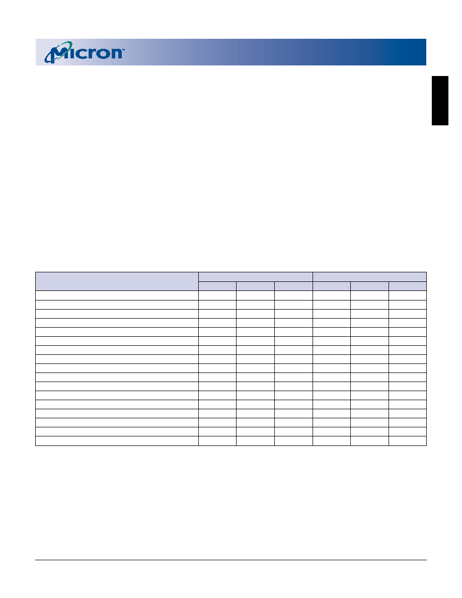
Table 6
Command State Machine Transition Table
)
n
o
i
t
i
t
r
a
p
t
n
e
s
e
r
p
e
h
t
f
o
e
t
a
t
s
t
x
e
n
d
n
a
(
n
o
i
t
i
t
r
a
p
t
n
e
s
e
r
p
e
h
t
o
t
t
u
p
n
i
d
n
a
m
m
o
C
t
n
e
s
e
r
p
e
h
t
f
o
e
t
a
t
s
t
n
e
s
e
r
P
n
o
i
t
i
t
r
a
p
e
t
a
t
s
t
n
e
s
e
r
P
r
e
h
t
o
e
h
t
f
o
n
o
i
t
i
t
r
a
p
h
F
2
k
c
o
L
n
w
o
d
m
r
i
f
n
o
c
h
1
0
k
c
o
L
m
r
i
f
n
o
c
h
0
C
P
T
O
p
u
t
e
s
h
0
6
k
c
o
l
n
U
/
k
c
o
L
n
w
o
d
k
c
o
L
/
h
8
9
d
a
e
R
y
r
e
u
q
h
0
9
d
a
e
R
e
c
i
v
e
d
D
I
h
0
5
r
a
e
l
C
s
u
t
a
t
s
r
e
t
s
i
g
e
r
h
0
7
d
a
e
R
s
u
t
a
t
s
h
0
B
m
a
r
g
o
r
P
e
s
a
r
E
/
d
n
e
p
s
u
s
h
0
D
,
m
r
i
f
n
o
c
E
B
,
e
m
u
s
e
r
E
/
P
m
r
i
f
n
o
c
B
L
U
h
0
2
e
s
a
r
E
p
u
t
e
s
h
0
4
/
h
0
1
/
A
P
A
m
a
r
g
o
r
P
p
u
t
e
s
h
F
F
d
a
e
R
y
a
r
r
a
7
R
S
a
t
a
D
n
e
h
w
d
a
e
r
e
t
a
t
S
e
d
o
M
y
a
r
r
a
d
a
e
R
k
c
o
L
d
a
e
R
y
r
e
u
q
d
a
e
R
D
I
d
a
e
R
y
a
r
r
a
d
a
e
R
s
u
t
a
t
s
y
a
r
r
a
d
a
e
R
1
y
a
r
r
A
y
a
r
r
A
d
a
e
R
1
p
u
t
e
S
2
y
s
u
B
y
a
r
r
a
d
a
e
R
P
T
O
p
u
t
e
s
y
a
r
r
a
d
a
e
R
e
s
a
r
E
p
u
t
e
s
m
a
r
g
o
r
P
p
u
t
e
s
d
a
e
R
y
a
r
r
a
3
e
l
d
I
y
a
r
r
a
d
a
e
R
y
a
r
r
a
d
a
e
R
4
e
s
a
r
E
d
n
e
p
s
u
s
y
a
r
r
a
d
a
e
R
5
.
g
o
r
P
d
n
e
p
s
u
s
y
a
r
r
a
d
a
e
R
k
c
o
L
d
a
e
R
y
r
e
u
q
d
a
e
R
D
I
d
a
e
R
y
a
r
r
a
d
a
e
R
s
u
t
a
t
s
y
a
r
r
a
d
a
e
R
1
I
F
C
y
r
e
u
Q
6
p
u
t
e
S
7
y
s
u
B
y
a
r
r
a
d
a
e
R
P
T
O
p
u
t
e
s
y
a
r
r
a
d
a
e
R
e
s
a
r
E
p
u
t
e
s
m
a
r
g
o
r
P
p
u
t
e
s
d
a
e
R
y
a
r
r
a
8
e
l
d
I
y
a
r
r
a
d
a
e
R
y
a
r
r
a
d
a
e
R
9
e
s
a
r
E
d
n
e
p
s
u
s
y
a
r
r
a
d
a
e
R
0
1
.
g
o
r
P
d
n
e
p
s
u
s
y
a
r
r
a
d
a
e
R
k
c
o
L
d
a
e
R
y
r
e
u
q
d
a
e
R
D
I
d
a
e
R
y
a
r
r
a
d
a
e
R
s
u
t
a
t
s
y
a
r
r
a
d
a
e
R
1
D
I
e
c
i
v
e
D
D
I
1
1
p
u
t
e
S
2
1
y
s
u
B
y
a
r
r
a
d
a
e
R
P
T
O
p
u
t
e
s
y
a
r
r
a
d
a
e
R
e
s
a
r
E
p
u
t
e
s
m
a
r
g
o
r
P
p
u
t
e
s
d
a
e
R
y
a
r
r
a
3
1
e
l
d
I
y
a
r
r
a
d
a
e
R
y
a
r
r
a
d
a
e
R
4
1
e
s
a
r
E
d
n
e
p
s
u
s
y
a
r
r
a
d
a
e
R
5
1
.
g
o
r
P
d
n
e
p
s
u
s
y
a
r
r
a
d
a
e
R
k
c
o
L
d
a
e
R
y
r
e
u
q
d
a
e
R
D
I
d
a
e
R
y
a
r
r
a
d
a
e
R
s
u
t
a
t
s
y
a
r
r
a
d
a
e
R
1
s
u
t
a
t
S
s
u
t
a
t
S
6
1
p
u
t
e
S
7
1
y
s
u
B
y
a
r
r
a
d
a
e
R
P
T
O
p
u
t
e
s
y
a
r
r
a
d
a
e
R
e
s
a
r
E
p
u
t
e
s
m
a
r
g
o
r
P
p
u
t
e
s
d
a
e
R
y
a
r
r
a
8
1
e
l
d
I
y
a
r
r
a
d
a
e
R
y
a
r
r
a
d
a
e
R
9
1
e
s
a
r
E
d
n
e
p
s
u
s
y
a
r
r
a
d
a
e
R
0
2
.
g
o
r
P
d
n
e
p
s
u
s
y
s
u
b
r
e
t
s
i
g
e
r
n
o
i
t
c
e
t
o
r
P
1
s
u
t
a
t
S
p
u
t
e
S
P
r
o
t
e
c
t
i
o
n
r
e
g
i
s
t
e
r
1
2
e
l
d
I
y
s
u
b
r
e
t
s
i
g
e
r
n
o
i
t
c
e
t
o
r
P
0
s
u
t
a
t
S
y
s
u
B
2
2
e
l
d
I
y
a
r
r
a
d
a
e
R
k
c
o
L
d
a
e
R
y
r
e
u
q
d
a
e
R
D
I
d
a
e
R
y
a
r
r
a
d
a
e
R
s
u
t
a
t
s
y
a
r
r
a
d
a
e
R
1
s
u
t
a
t
S
e
n
o
D
3
2
p
u
t
e
S
4
2
y
s
u
B
y
a
r
r
a
d
a
e
R
P
T
O
p
u
t
e
s
k
c
o
L
d
a
e
R
y
r
e
u
q
d
a
e
R
D
I
d
a
e
R
y
a
r
r
a
d
a
e
R
s
u
t
a
t
s
y
a
r
r
a
d
a
e
R
e
s
a
r
E
p
u
t
e
s
m
a
r
g
o
r
P
p
u
t
e
s
d
a
e
R
y
a
r
r
a
1
s
u
t
a
t
S
e
n
o
D
5
2
e
l
d
I
y
a
r
r
a
d
a
e
R
y
a
r
r
a
d
a
e
R
6
2
e
s
a
r
E
d
n
e
p
s
u
s
y
a
r
r
a
d
a
e
R
7
2
.
g
o
r
P
d
n
e
p
s
u
s
(continued on next page)
FLASH
16
4 Meg x 16 Asynchronous/Page Flash 512K x 16 SRAM Combo Memory
Micron Technology, Inc., reserves the right to change products or specifications without notice.
MT28C6428P20_3.p65 ≠ Rev. 3, Pub. 7/02
©2002, Micron Technology, Inc.
4 MEG x 16 ASYNCHRONOUS/PAGE FLASH
512K x 16 SRAM COMBO MEMORY
ADVANCE
Table 6
Command State Machine Transition Table (continued)
)
n
o
i
t
i
t
r
a
p
t
n
e
s
e
r
p
e
h
t
f
o
e
t
a
t
s
t
x
e
n
d
n
a
(
n
o
i
t
i
t
r
a
p
t
n
e
s
e
r
p
e
h
t
o
t
t
u
p
n
i
d
n
a
m
m
o
C
t
n
e
s
e
r
p
e
h
t
f
o
e
t
a
t
s
t
n
e
s
e
r
P
n
o
i
t
i
t
r
a
p
f
o
e
t
a
t
s
t
n
e
s
e
r
P
r
e
h
t
o
e
h
t
n
o
i
t
i
t
r
a
p
h
F
2
k
c
o
L
n
w
o
d
m
r
i
f
n
o
c
h
1
0
k
c
o
L
m
r
i
f
n
o
c
H
0
C
P
T
O
p
u
t
e
s
h
0
6
k
c
o
l
n
U
/
k
c
o
L
n
w
o
d
k
c
o
L
/
h
8
9
d
a
e
R
y
r
e
u
q
h
0
9
d
a
e
R
D
I
e
c
i
v
e
d
h
0
5
r
a
e
l
C
s
u
t
a
t
s
r
e
t
s
i
g
e
r
h
0
7
d
a
e
R
s
u
t
a
t
s
h
0
B
m
a
r
g
o
r
P
e
s
a
r
E
/
d
n
e
p
s
u
s
h
0
D
,
m
r
i
f
n
o
c
E
B
,
e
m
u
s
e
r
E
/
P
m
r
i
f
n
o
c
B
L
U
h
0
2
e
s
a
r
E
p
u
t
e
s
h
0
4
/
h
0
1
/
A
P
A
m
a
r
g
o
r
P
p
u
t
e
s
h
F
F
d
a
e
R
y
a
r
r
a
7
R
S
a
t
a
D
n
e
h
w
d
a
e
r
e
t
a
t
S
e
d
o
M
B
L
U
/
B
L
k
c
o
L
L
B
L
U
/
B
L
k
c
o
L
1
s
u
t
a
t
S
p
u
t
e
S
k
c
o
L
8
2
y
n
A
e
t
a
t
s
y
a
r
r
a
d
a
e
R
k
c
o
L
d
a
e
R
y
r
e
u
q
D
I
d
a
e
R
d
a
e
R
y
a
r
r
a
d
a
e
R
s
u
t
a
t
s
y
a
r
r
a
d
a
e
R
1
s
u
t
a
t
S
r
o
r
r
E
9
2
p
u
t
e
S
0
3
y
s
u
B
y
a
r
r
a
d
a
e
R
P
T
O
p
u
t
e
s
y
a
r
r
a
d
a
e
R
e
s
a
r
E
p
u
t
e
s
m
a
r
g
o
r
P
p
u
t
e
s
d
a
e
R
y
a
r
r
a
1
3
e
l
d
I
y
a
r
r
a
d
a
e
R
y
a
r
r
a
d
a
e
R
2
3
e
s
a
r
E
d
n
e
p
s
u
s
y
a
r
r
a
d
a
e
R
3
3
.
g
o
r
P
d
n
e
p
s
u
s
y
a
r
r
a
d
a
e
R
k
c
o
L
d
a
e
R
y
r
e
u
q
D
I
d
a
e
R
d
a
e
R
y
a
r
r
a
d
a
e
R
s
u
t
a
t
s
y
a
r
r
a
d
a
e
R
1
s
u
t
a
t
S
/
k
c
o
L
k
c
o
l
n
U
4
3
p
u
t
e
S
5
3
y
s
u
B
y
a
r
r
a
d
a
e
R
P
T
O
p
u
t
e
s
y
a
r
r
a
d
a
e
R
e
s
a
r
E
p
u
t
e
s
m
a
r
g
o
r
P
p
u
t
e
s
d
a
e
R
y
a
r
r
a
6
3
e
l
d
I
y
a
r
r
a
d
a
e
R
y
a
r
r
a
d
a
e
R
7
3
e
s
a
r
E
d
n
e
p
s
u
s
y
a
r
r
a
d
a
e
R
8
3
.
g
o
r
P
d
n
e
p
s
u
s
y
s
u
B
m
a
r
g
o
r
P
1
s
u
t
a
t
S
p
u
t
e
S
m
a
r
g
o
r
P
9
3
y
n
A
e
t
a
t
s
y
s
u
B
m
a
r
g
o
r
P
d
a
e
r
S
P
y
s
u
b
m
a
r
g
o
r
P
0
s
u
t
a
t
S
y
s
u
B
0
4
e
l
d
I
y
a
r
r
a
d
a
e
R
k
c
o
L
d
a
e
R
y
r
e
u
q
D
I
d
a
e
R
d
a
e
R
y
a
r
r
a
d
a
e
R
s
u
t
a
t
s
y
a
r
r
a
d
a
e
R
1
s
u
t
a
t
S
e
n
o
D
1
4
p
u
t
e
S
2
4
y
s
u
B
y
a
r
r
a
d
a
e
R
P
T
O
p
u
t
e
s
y
a
r
r
a
d
a
e
R
e
s
a
r
E
p
u
t
e
s
m
a
r
g
o
r
P
p
u
t
e
s
d
a
e
R
y
a
r
r
a
3
4
e
l
d
I
y
a
r
r
a
d
a
e
R
y
a
r
r
a
d
a
e
R
4
4
e
s
a
r
E
d
n
e
p
s
u
s
y
a
r
r
a
d
a
e
R
5
4
.
g
o
r
P
d
n
e
p
s
u
s
d
a
e
r
d
n
e
p
s
u
s
m
a
r
g
o
r
P
y
a
r
r
a
k
c
o
L
m
a
r
g
o
r
P
d
n
e
p
s
u
s
d
a
e
r
y
r
e
u
q
m
a
r
g
o
r
P
d
n
e
p
s
u
s
D
I
d
a
e
r
m
a
r
g
o
r
P
d
n
e
p
s
u
s
d
a
e
r
y
a
r
r
a
m
a
r
g
o
r
P
d
n
e
p
s
u
s
d
a
e
r
s
u
t
a
t
s
m
a
r
g
o
r
P
d
n
e
p
s
u
s
d
a
e
r
y
a
r
r
a
y
s
u
b
m
a
r
g
o
r
P
d
a
e
r
d
n
e
p
s
u
s
m
a
r
g
o
r
P
y
a
r
r
a
1
s
u
t
a
t
S
d
a
e
R
s
u
t
a
t
s
m
a
r
g
o
r
P
d
n
e
p
s
u
s
6
4
p
u
t
e
S
7
4
e
l
d
I
8
4
e
s
a
r
E
d
n
e
p
s
u
s
(continued on next page)

FLASH
17
4 Meg x 16 Asynchronous/Page Flash 512K x 16 SRAM Combo Memory
Micron Technology, Inc., reserves the right to change products or specifications without notice.
MT28C6428P20_3.p65 ≠ Rev. 3, Pub. 7/02
©2002, Micron Technology, Inc.
4 MEG x 16 ASYNCHRONOUS/PAGE FLASH
512K x 16 SRAM COMBO MEMORY
ADVANCE
Table 6
Command State Machine Transition Table (continued)
)
n
o
i
t
i
t
r
a
p
t
n
e
s
e
r
p
e
h
t
f
o
e
t
a
t
s
t
x
e
n
d
n
a
(
n
o
i
t
i
t
r
a
p
t
n
e
s
e
r
p
e
h
t
o
t
t
u
p
n
i
d
n
a
m
m
o
C
t
n
e
s
e
r
p
e
h
t
f
o
e
t
a
t
s
t
n
e
s
e
r
P
n
o
i
t
i
t
r
a
p
e
t
a
t
s
t
n
e
s
e
r
P
r
e
h
t
o
e
h
t
f
o
n
o
i
t
i
t
r
a
p
h
F
2
k
c
o
L
n
w
o
d
m
r
i
f
n
o
c
h
1
0
k
c
o
L
m
r
i
f
n
o
c
h
0
C
P
T
O
p
u
t
e
s
h
0
6
k
c
o
l
n
U
/
k
c
o
L
n
w
o
d
k
c
o
L
/
h
8
9
d
a
e
R
y
r
e
u
q
h
0
9
d
a
e
R
D
I
e
c
i
v
e
d
h
0
5
r
a
e
l
C
s
u
t
a
t
s
r
e
t
s
i
g
e
r
h
0
7
d
a
e
R
s
u
t
a
t
s
h
0
B
m
a
r
g
o
r
P
e
s
a
r
E
/
d
n
e
p
s
u
s
h
0
D
,
m
r
i
f
n
o
c
E
B
,
e
m
u
s
e
r
E
/
P
m
r
i
f
n
o
c
B
L
U
h
0
2
e
s
a
r
E
p
u
t
e
s
h
0
4
/
h
0
1
/
A
P
A
m
a
r
g
o
r
P
p
u
t
e
s
h
F
F
d
a
e
R
y
a
r
r
a
7
R
S
a
t
a
D
n
e
h
w
d
a
e
r
e
t
a
t
S
e
d
o
M
d
n
e
p
s
u
s
m
a
r
g
o
r
P
y
a
r
r
a
d
a
e
r
k
c
o
L
m
a
r
g
o
r
P
d
n
e
p
s
u
s
d
a
e
r
y
r
e
u
q
m
a
r
g
o
r
P
d
n
e
p
s
u
s
D
I
d
a
e
r
m
a
r
g
o
r
P
d
n
e
p
s
u
s
d
a
e
r
y
a
r
r
a
m
a
r
g
o
r
P
d
n
e
p
s
u
s
d
a
e
r
s
u
t
a
t
s
m
a
r
g
o
r
P
d
n
e
p
s
u
s
d
a
e
r
y
a
r
r
a
y
s
u
b
m
a
r
g
o
r
P
d
n
e
p
s
u
s
m
a
r
g
o
r
P
y
a
r
r
a
d
a
e
r
1
y
a
r
r
A
d
a
e
R
y
a
r
r
a
m
a
r
g
o
r
P
d
n
e
p
s
u
s
9
4
p
u
t
e
S
0
5
e
l
d
I
1
5
e
s
a
r
E
d
n
e
p
s
u
s
d
n
e
p
s
u
s
m
a
r
g
o
r
P
y
a
r
r
a
d
a
e
r
k
c
o
L
m
a
r
g
o
r
P
d
n
e
p
s
u
s
d
a
e
r
y
r
e
u
q
m
a
r
g
o
r
P
d
n
e
p
s
u
s
D
I
d
a
e
r
m
a
r
g
o
r
P
d
n
e
p
s
u
s
d
a
e
r
y
a
r
r
a
m
a
r
g
o
r
P
d
n
e
p
s
u
s
d
a
e
r
s
u
t
a
t
s
m
a
r
g
o
r
P
d
n
e
p
s
u
s
d
a
e
r
y
a
r
r
a
y
s
u
b
m
a
r
g
o
r
P
d
n
e
p
s
u
s
m
a
r
g
o
r
P
y
a
r
r
a
d
a
e
r
1
D
I
D
I
d
a
e
R
2
5
p
u
t
e
S
3
5
e
l
d
I
4
5
e
s
a
r
E
d
n
e
p
s
u
s
d
n
e
p
s
u
s
m
a
r
g
o
r
P
y
a
r
r
a
d
a
e
r
k
c
o
L
m
a
r
g
o
r
P
d
n
e
p
s
u
s
d
a
e
r
y
r
e
u
q
m
a
r
g
o
r
P
d
n
e
p
s
u
s
D
I
d
a
e
r
m
a
r
g
o
r
P
d
n
e
p
s
u
s
d
a
e
r
y
a
r
r
a
m
a
r
g
o
r
P
d
n
e
p
s
u
s
d
a
e
r
s
u
t
a
t
s
m
a
r
g
o
r
P
d
n
e
p
s
u
s
d
a
e
r
y
a
r
r
a
y
s
u
b
m
a
r
g
o
r
P
d
n
e
p
s
u
s
m
a
r
g
o
r
P
y
a
r
r
a
d
a
e
r
1
I
F
C
d
a
e
R
y
r
e
u
Q
5
5
p
u
t
e
S
6
5
e
l
d
I
7
5
e
s
a
r
E
d
n
e
p
s
u
s
B
L
U
/
B
L
r
o
r
r
e
e
s
a
r
E
e
s
a
r
E
r
o
r
r
e
y
s
u
b
e
s
a
r
E
r
o
r
r
e
e
s
a
r
E
1
s
u
t
a
t
S
p
u
t
e
S
e
s
a
r
E
8
5
e
l
d
I
y
a
r
r
a
d
a
e
R
k
c
o
L
d
a
e
R
y
r
e
u
q
D
I
d
a
e
R
d
a
e
R
y
a
r
r
a
d
a
e
R
s
u
t
a
t
s
y
a
r
r
a
d
a
e
R
1
s
u
t
a
t
S
r
o
r
r
E
9
5
p
u
t
e
S
0
6
y
s
u
B
y
a
r
r
a
d
a
e
R
P
T
O
p
u
t
e
s
y
a
r
r
a
d
a
e
R
e
s
a
r
E
p
u
t
e
s
m
a
r
g
o
r
P
p
u
t
e
s
d
a
e
R
y
a
r
r
a
1
6
e
l
d
I
y
a
r
r
a
d
a
e
R
y
a
r
r
a
d
a
e
R
2
6
e
s
a
r
E
d
n
e
p
s
u
s
y
a
r
r
a
d
a
e
R
3
6
.
g
o
r
P
d
n
e
p
s
u
s
y
a
r
r
a
d
a
e
R
k
c
o
L
d
a
e
R
y
r
e
u
q
D
I
d
a
e
R
d
a
e
R
y
a
r
r
a
d
a
e
R
s
u
t
a
t
s
y
a
r
r
a
d
a
e
R
1
s
u
t
a
t
S
e
n
o
D
4
6
p
u
t
e
S
5
6
y
s
u
B
y
a
r
r
a
d
a
e
R
P
T
O
p
u
t
e
s
y
a
r
r
a
d
a
e
R
e
s
a
r
E
m
a
r
g
o
r
P
p
u
t
e
s
d
a
e
R
y
a
r
r
a
6
6
e
l
d
I
y
a
r
r
a
d
a
e
R
y
a
r
r
a
d
a
e
R
7
6
e
s
a
r
E
d
n
e
p
s
u
s
y
a
r
r
a
d
a
e
R
8
6
.
g
o
r
P
d
n
e
p
s
u
s
y
s
u
b
e
s
a
r
e
k
c
o
l
B
d
a
e
r
S
E
s
u
t
a
t
s
y
s
u
b
e
s
a
r
E
0
s
u
t
a
t
S
y
s
u
B
9
6
e
l
d
I
(continued on next page)
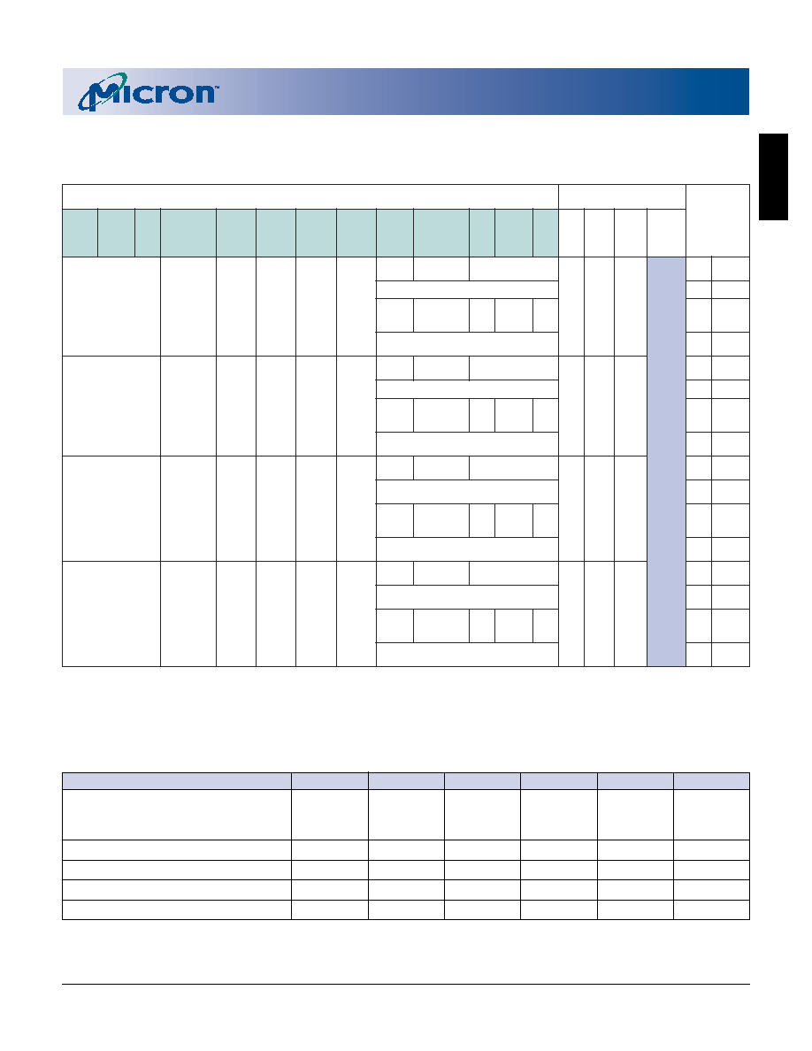
FLASH
18
4 Meg x 16 Asynchronous/Page Flash 512K x 16 SRAM Combo Memory
Micron Technology, Inc., reserves the right to change products or specifications without notice.
MT28C6428P20_3.p65 ≠ Rev. 3, Pub. 7/02
©2002, Micron Technology, Inc.
4 MEG x 16 ASYNCHRONOUS/PAGE FLASH
512K x 16 SRAM COMBO MEMORY
ADVANCE
Table 6
Command State Machine Transition Table (continued)
)
n
o
i
t
i
t
r
a
p
t
n
e
s
e
r
p
e
h
t
f
o
e
t
a
t
s
t
x
e
n
d
n
a
(
n
o
i
t
i
t
r
a
p
t
n
e
s
e
r
p
e
h
t
o
t
t
u
p
n
i
d
n
a
m
m
o
C
t
n
e
s
e
r
p
e
h
t
f
o
e
t
a
t
s
t
n
e
s
e
r
P
n
o
i
t
i
t
r
a
p
e
t
a
t
s
t
n
e
s
e
r
P
r
e
h
t
o
e
h
t
f
o
n
o
i
t
i
t
r
a
p
h
F
2
k
c
o
L
n
w
o
d
m
r
i
f
n
o
c
h
1
0
`
k
c
o
L
m
r
i
f
n
o
c
h
0
C
P
T
O
p
u
t
e
s
h
0
6
k
c
o
l
n
U
/
k
c
o
L
n
w
o
d
k
c
o
L
/
h
8
9
d
a
e
R
y
r
e
u
q
h
0
9
d
a
e
R
D
I
e
c
i
v
e
d
h
0
5
r
a
e
l
C
s
u
t
a
t
s
r
e
t
s
i
g
e
r
h
0
7
d
a
e
R
s
u
t
a
t
s
h
0
B
m
a
r
g
o
r
P
e
s
a
r
E
/
d
n
e
p
s
u
s
h
0
D
,
m
r
i
f
n
o
c
E
B
,
e
m
u
s
e
r
E
/
P
m
r
i
f
n
o
c
B
L
U
h
0
2
e
s
a
r
E
p
u
t
e
s
h
0
4
/
h
0
1
/
A
P
A
m
a
r
g
o
r
P
p
u
t
e
s
h
F
F
d
a
e
R
y
a
r
r
a
7
R
S
a
t
a
D
n
e
h
w
d
a
e
r
e
t
a
t
S
e
d
o
M
y
a
r
r
a
d
a
e
r
d
n
e
p
s
u
s
e
s
a
r
E
k
c
o
L
e
s
a
r
E
d
n
e
p
s
u
s
d
a
e
r
y
r
e
u
q
e
s
a
r
E
d
n
e
p
s
u
s
D
I
d
a
e
r
e
s
a
r
E
d
n
e
p
s
u
s
d
a
e
r
y
a
r
r
a
e
s
a
r
E
d
n
e
p
s
u
s
d
a
e
r
s
u
t
a
t
s
d
a
e
r
S
E
y
a
r
r
a
y
s
u
b
e
s
a
r
E
d
n
e
p
s
u
s
e
s
a
r
E
y
a
r
r
a
d
a
e
r
1
s
u
t
a
t
S
d
a
e
R
s
u
t
a
t
s
e
s
a
r
E
d
n
e
p
s
u
s
0
7
p
u
t
e
S
y
a
r
r
a
d
a
e
r
d
n
e
p
s
u
s
e
s
a
r
E
1
7
y
s
u
B
d
a
e
r
S
E
y
a
r
r
a
y
s
u
b
e
s
a
r
E
S
E
d
a
e
r
y
a
r
r
a
.
g
o
r
P
p
u
t
e
s
S
E
d
a
e
r
y
a
r
r
a
2
7
e
l
d
I
y
a
r
r
a
d
a
e
r
d
n
e
p
s
u
s
e
s
a
r
E
3
7
.
g
o
r
P
d
n
e
p
s
u
s
y
a
r
r
a
d
a
e
r
d
n
e
p
s
u
s
e
s
a
r
E
k
c
o
L
e
s
a
r
E
d
n
e
p
s
u
s
d
a
e
r
y
r
e
u
q
e
s
a
r
E
d
n
e
p
s
u
s
D
I
d
a
e
r
e
s
a
r
E
d
n
e
p
s
u
s
d
a
e
r
y
a
r
r
a
e
s
a
r
E
d
n
e
p
s
u
s
d
a
e
r
s
u
t
a
t
s
d
a
e
r
S
E
y
a
r
r
a
y
s
u
b
e
s
a
r
E
d
a
e
r
d
n
e
p
s
u
s
e
s
a
r
E
y
a
r
r
a
1
y
a
r
r
A
d
a
e
R
a
r
r
a
y
4
7
p
u
t
e
S
y
a
r
r
a
d
a
e
r
d
n
e
p
s
u
s
e
s
a
r
E
5
7
y
s
u
B
d
a
e
r
S
E
y
a
r
r
a
y
s
u
b
e
s
a
r
E
S
E
d
a
e
r
y
a
r
r
a
.
g
o
r
P
p
u
t
e
s
S
E
d
a
e
r
y
a
r
r
a
6
7
e
l
d
I
y
a
r
r
a
d
a
e
r
d
n
e
p
s
u
s
e
s
a
r
E
7
7
.
g
o
r
P
d
n
e
p
s
u
s
y
a
r
r
a
d
a
e
r
d
n
e
p
s
u
s
e
s
a
r
E
k
c
o
L
e
s
a
r
E
d
n
e
p
s
u
s
d
a
e
r
y
r
e
u
q
e
s
a
r
E
d
n
e
p
s
u
s
D
I
d
a
e
r
e
s
a
r
E
d
n
e
p
s
u
s
d
a
e
r
y
a
r
r
a
e
s
a
r
E
d
n
e
p
s
u
s
d
a
e
r
s
u
t
a
t
s
d
a
e
r
S
E
y
a
r
r
a
y
s
u
b
e
s
a
r
E
d
n
e
p
s
u
s
e
s
a
r
E
y
a
r
r
a
d
a
e
r
1
D
I
d
a
e
R
D
I
8
7
p
u
t
e
S
y
a
r
r
a
d
a
e
r
d
n
e
p
s
u
s
e
s
a
r
E
9
7
y
s
u
B
d
a
e
r
S
E
y
a
r
r
a
y
s
u
b
e
s
a
r
E
S
E
d
a
e
r
y
a
r
r
a
.
g
o
r
P
p
u
t
e
s
S
E
d
a
e
r
y
a
r
r
a
0
8
e
l
d
I
y
a
r
r
a
d
a
e
r
d
n
e
p
s
u
s
e
s
a
r
E
1
8
.
g
o
r
P
d
n
e
p
s
u
s
y
a
r
r
a
d
a
e
r
d
n
e
p
s
u
s
e
s
a
r
E
k
c
o
L
e
s
a
r
E
d
n
e
p
s
u
s
d
a
e
r
y
r
e
u
q
e
s
a
r
E
d
n
e
p
s
u
s
D
I
d
a
e
r
e
s
a
r
E
d
n
e
p
s
u
s
d
a
e
r
y
a
r
r
a
e
s
a
r
E
d
n
e
p
s
u
s
d
a
e
r
s
u
t
a
t
s
d
a
e
r
S
E
y
a
r
r
a
y
s
u
b
e
s
a
r
E
d
n
e
p
s
u
s
e
s
a
r
E
y
a
r
r
a
d
a
e
r
1
I
F
C
d
a
e
R
y
r
e
u
q
2
8
p
u
t
e
S
y
a
r
r
a
d
a
e
r
d
n
e
p
s
u
s
e
s
a
r
E
3
8
y
s
u
B
d
a
e
r
S
E
y
a
r
r
a
y
s
u
b
e
s
a
r
E
S
E
d
a
e
r
y
a
r
r
a
.
g
o
r
P
p
u
t
e
s
S
E
d
a
e
r
y
a
r
r
a
4
8
e
l
d
I
y
a
r
r
a
d
a
e
r
d
n
e
p
s
u
s
e
s
a
r
E
5
8
.
g
o
r
P
d
n
e
p
s
u
s
Table 7
Bus Operations
MODE
F_RP#
F_CE#
F_OE#
F_WE#
ADDRESS DQ0≠DQ15
Read (array, status registers,
V
IH
V
IL
V
IL
V
IH
X
D
OUT
device identification register, or
query)
Standby
V
IH
V
IH
X
X
X
High-Z
Output Disable
V
IL
V
IH
V
IH
V
IH
X
High-Z
Reset
V
IL
X
X
X
X
High-Z
Write
V
IH
V
IL
V
IH
V
IL
X
D
IN

FLASH
19
4 Meg x 16 Asynchronous/Page Flash 512K x 16 SRAM Combo Memory
Micron Technology, Inc., reserves the right to change products or specifications without notice.
MT28C6428P20_3.p65 ≠ Rev. 3, Pub. 7/02
©2002, Micron Technology, Inc.
4 MEG x 16 ASYNCHRONOUS/PAGE FLASH
512K x 16 SRAM COMBO MEMORY
ADVANCE
For in-system programming, when 0.9V
F_V
PP
2.2V, the APA and the 32 single-word buffer signifi-
cantly improve both the system throughput and the
average programming time when compared with stan-
dard programming practices. The accelerated pro-
gramming functionality executes and verifies the APA
without microprocessor intervention. This relieves the
microprocessor from constantly monitoring the
progress of the programming and erase activity, free-
ing up valuable memory bus bandwidth. This increases
the system throughput.
ERASE OPERATIONS
An ERASE operation must be used to initialize all
bits in an array block to "1s." After BLOCK ERASE con-
firm is issued, the CSM responds only to an ERASE
SUSPEND command until the WSM completes its task.
Block erasure inside the memory array sets all bits
within the address block to logic 1s. Erase is accom-
plished only by blocks; data at single address locations
within the array cannot be erased individually. The
block to be erased is selected by using any valid ad-
dress within that block. Block erasure is initiated by a
command sequence to the CSM: BLOCK ERASE SETUP
(20h) followed by BLOCK ERASE CONFIRM (D0h) (see
Table 5). A two-command erase sequence protects
against accidental erasure of memory contents.
When the BLOCK ERASE CONFIRM command is
complete, the WSM automatically executes a sequence
of events to complete the block erasure. During this
sequence, the block is programmed with logic 0s, data
is verified, all bits in the block are erased, and finally
verification is performed to ensure that all bits are cor-
rectly erased. Monitoring of the ERASE operation is
possible through the status register (see the Status
Register section).
During the execution of an ERASE operation, the
ERASE SUSPEND command (B0h) can be entered to
direct the WSM to suspend the ERASE operation. Once
the WSM has reached the suspend state, it allows the
CSM to respond only to the READ ARRAY, READ
STATUS REGISTER, READ QUERY, READ CHIP PRO-
TECTION CONFIGURATION, PROGRAM SETUP, PRO-
GRAM RESUME, ERASE RESUME and LOCK SETUP
(see the Block Locking section). During the ERASE SUS-
PEND operation, array data must be read from a block
other than the one being erased. To resume the ERASE
operation, an ERASE RESUME command (D0h) must
be issued to cause the CSM to clear the suspend state
previously set (see Figure 8). It is also possible that an
ERASE in any bank can be suspended and a WRITE to
another block in the same bank can be initiated. After
PROGRAMMING OPERATIONS
There are two CSM commands for programming:
PROGRAM SETUP and ACCELERATED PROGRAM-
MING ALGORITHM (see Table 3).
PROGRAM SETUP COMMAND
After the 40h command code is entered on DQ0≠
DQ7, the WSM takes over and correctly sequences the
device to complete the PROGRAM operation. The
WRITE operation may be monitored through the sta-
tus register (see the Status Register section). During
this time, the CSM will only respond to a PROGRAM
SUSPEND command until the PROGRAM operation
has been completed, after which time, all commands
to the CSM become valid again. The PROGRAM opera-
tion can be suspended by issuing a PROGRAM SUS-
PEND command (B0h).
Once the WSM reaches the suspend state, it allows
the CSM to respond only to READ ARRAY, READ STA-
TUS REGISTER, READ PROTECTION CONFIGURA-
TION, READ QUERY, PROGRAM SETUP, or PROGRAM
RESUME. During the PROGRAM SUSPEND operation,
array data should be read from an address other than
the one being programmed. To resume the PROGRAM
operation, a PROGRAM RESUME command (D0h) must
be issued to cause the CSM to clear the suspend state
previously set (see Figure 4 for programming operation
and Figure 5 for program suspend and program re-
sume).
Taking RP# to V
IL
during programming aborts the
PROGRAM operation.
ACCELERATED PROGRAMMING ALGORITHM
The accelerated programming algorithm (APA) is
intended for in-system and in-factory use. Its 32
single-word internal buffer enables fast data stream
programming.
The APA is activated when the WSM executes com-
mand code 10h. Upon activation, the word address
and the data sequences must be provided to the WSM,
without polling SR7. The same starting address must
be provided for each data word. After all 32 sequences
are issued, the status register reports a busy condition.
Figure 6 shows the APA flowchart.
If the data stream is shorter than 32 words, use
FFFFh to fill in the missing data. Also, be sure the start-
ing address is aligned with a 32-word boundary.
The APA is fully concurrent. For example, it can be
interrupted and resumed during programming. When
loading the programming buffer, only a read access in
the other bank is allowed.
For in-factory programming, the APA, along with an
optimized set of programming parameters, minimizes
chip programming time when 11.4V
F_V
PP
12.6V.
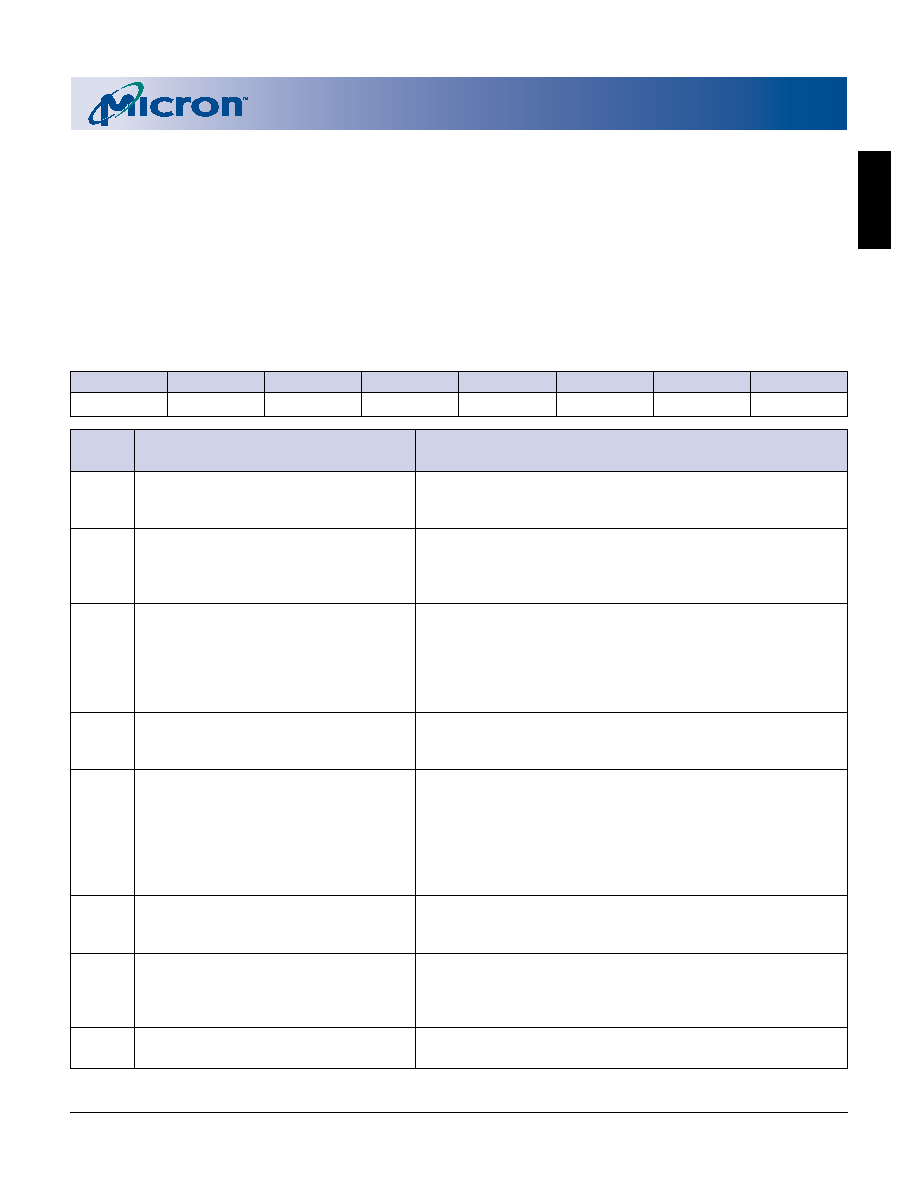
FLASH
20
4 Meg x 16 Asynchronous/Page Flash 512K x 16 SRAM Combo Memory
Micron Technology, Inc., reserves the right to change products or specifications without notice.
MT28C6428P20_3.p65 ≠ Rev. 3, Pub. 7/02
©2002, Micron Technology, Inc.
4 MEG x 16 ASYNCHRONOUS/PAGE FLASH
512K x 16 SRAM COMBO MEMORY
ADVANCE
STATUS
BIT #
STATUS REGISTER BIT
DESCRIPTION
SR7
WRITE STATE MACHINE STATUS (WSMS) Check write state machine bit first to determine word
1 = Ready
program or block erase completion, before checking
0 = Busy
program or erase status bits.
SR6
ERASE SUSPEND STATUS (ESS)
When ERASE SUSPEND is issued, WSM halts execution and
1 = BLOCK ERASE Suspended
sets both WSMS and ESS bits to "1." ESS bit remains set to
0 = BLOCK ERASE in
"1" until an ERASE RESUME command is issued.
Progress/Completed
SR5
ERASE/CHECK BLOCK ERASE
When this bit is set to "1" and ERASE CONFIRM is issued, WSM
STATUS (ES)
has applied the maximum number of erase pulses to the
1 = Error in BLOCK ERASE/
block and is still unable to verify successful block erasure.
CHECK BLOCK ERASE
When this bit is set to "1" and CHECK BLOCK ERASE CONFIRM
0 = Successful BLOCK ERASE
is issued, WSM has checked the block for its erase state, and
the block is not erased.
SR4
PROGRAM STATUS (PS)
When this bit is set to "1," WSM has attempted but failed to
1 = Error in PROGRAM
program a word.
0 = Successful PROGRAM
SR3
F_V
PP
STATUS (V
PP
S)
The F_V
PP
status bit does not provide continuous indication
1 = F_V
PP
Low Detect, Operation Abort of the F_V
PP
level. The WSM interrogates the F_V
PP
level only
0 = F_V
PP
= OK
after the program or erase command sequences have been
entered and informs the system if F_V
PP
< 0.9V. The F_V
PP
level is also checked before the PROGRAM/ERASE operation
is verified by the WSM. A factory option allows PROGRAM or
ERASE at 0V, in which case SR3 is held at "0."
SR2
PROGRAM SUSPEND STATUS (PSS)
When PROGRAM SUSPEND is issued, WSM halts execution
1 = PROGRAM Suspended
and sets both WSM and PSS bits to "1." PSS bit remains set to
0 = PROGRAM in Progress/Completed
"1" until a PROGRAM RESUME command is issued.
SR1
BLOCK LOCK STATUS (BLS)
If a PROGRAM or ERASE operation is attempted to one of
1 = PROGRAM/ERASE Attempted on a
the locked blocks, this is set by the WSM. The operation
Locked Block; Operation Aborted
specified is aborted, and the device is returned to read status
0 = No Operation to Locked Blocks
mode.
SR0
RESERVED FOR FUTURE
This bit is reserved for future use.
ENHANCEMENT
Table 8
Status Register Bit Definition
WSMS
ESS
ES
PS
V
PP
S
PSS
BLS
R
7
6
5
4
3
2
1
0
the completion of a WRITE, an ERASE can be resumed
by writing an ERASE RESUME command.
After an ERASE command completion, it is possible
to check if the block has been erased successfully, us-
ing the CHECK BLOCK ERASE command. Two bus
cycles are required for this operation: one to set up the
CHECK BLOCK ERASE and the second one to start the
execution of the command. If after the operation the
bit SR5 is set to 0 the operation has been completed
succesfully, if it is set to 1, there has been an error
during the BLOCK ERASE operation.
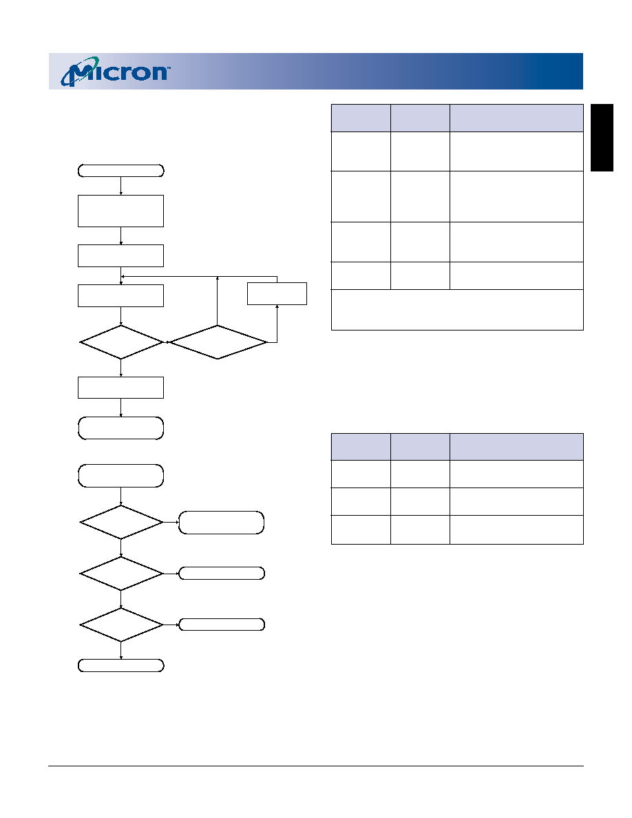
FLASH
21
4 Meg x 16 Asynchronous/Page Flash 512K x 16 SRAM Combo Memory
Micron Technology, Inc., reserves the right to change products or specifications without notice.
MT28C6428P20_3.p65 ≠ Rev. 3, Pub. 7/02
©2002, Micron Technology, Inc.
4 MEG x 16 ASYNCHRONOUS/PAGE FLASH
512K x 16 SRAM COMBO MEMORY
ADVANCE
Figure 4
Automated Word Programming
Flowchart
NOTE: 1. Full status register check can be done after each word or after a sequence of words.
2. SR3 must be cleared before attempting additional PROGRAM/ERASE operations.
3. SR4 is cleared only by the CLEAR STATUS REGISTER command, but it does not prevent additional program operation
attempts.
BUS
OPERATION COMMAND COMMENTS
WRITE
WRITE
Data =
40h
PROGRAM
Addr =
Address of word to be
SETUP
programmed
WRITE
WRITE
Data =
Word to be
DATA
programmed
Addr =
Address of word to be
programmed
READ
Status register data;
toggle OE# or CE# to update
status register.
Standby
Check SR7
1 = Ready, 0 = Busy
Repeat for subsequent words.
Write FFh after the last word programming operation
to reset the device to read array mode.
BUS
OPERATION COMMAND COMMENTS
Standby
Check SR1
1 = Detect locked block
Standby
Check SR3
2
1 = Detect F_V
PP
low
Standby
Check SR4
3
1 = Word program error
YES
NO
Full Status Register
Check (optional)
NO
YES
PROGRAM
SUSPEND?
SR7 = 1?
Issue PROGRAM SETUP
Command and
Word Address
Start
Word Program Passed
V
PP
Range Error
Word Program Failed
FULL STATUS REGISTER CHECK FLOW
Read Status Register
Bits
Issue Word Address
and Word Data
PROGRAM
SUSPEND Loop
1
YES
NO
SR1 = 0?
YES
NO
SR3 = 0?
YES
NO
SR4 = 0?
Word Program
Completed
Read Status Register
Bits
PROGRAM Attempted
on a Locked Block
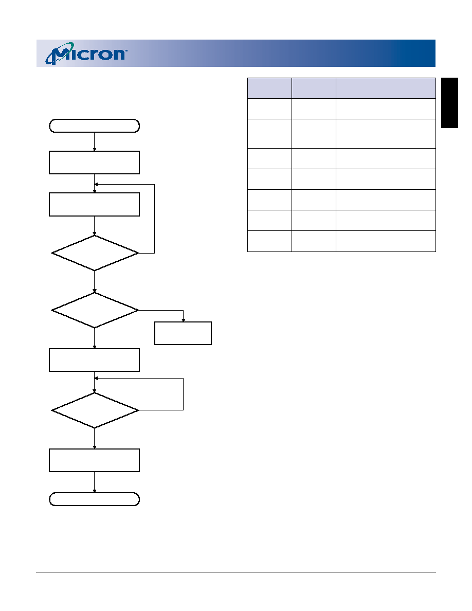
FLASH
22
4 Meg x 16 Asynchronous/Page Flash 512K x 16 SRAM Combo Memory
Micron Technology, Inc., reserves the right to change products or specifications without notice.
MT28C6428P20_3.p65 ≠ Rev. 3, Pub. 7/02
©2002, Micron Technology, Inc.
4 MEG x 16 ASYNCHRONOUS/PAGE FLASH
512K x 16 SRAM COMBO MEMORY
ADVANCE
Issue READ ARRAY
Command
PROGRAM
Complete
Finished
Reading
?
Issue PROGRAM
RESUME Command
YES
YES
NO
NO
SR2 = 1?
Start
PROGRAM Resumed
Read Status Register
Bits
Issue PROGRAM
SUSPEND Command
YES
NO
SR7 = 1?
Figure 5
PROGRAM SUSPEND/
PROGRAM RESUME Flowchart
BUS
OPERATION COMMAND COMMENTS
WRITE
PROGRAM
Data = B0h
SUSPEND
READ
Status register data;
toggle OE# or CE# to update
status register.
Standby
Check SR7
1 = Ready
Standby
Check SR2
1 = Suspended
WRITE
READ
Data = FFh
MEMORY
READ
Read data from block other
than that being programmed.
WRITE
PROGRAM
Data = D0h
RESUME

FLASH
23
4 Meg x 16 Asynchronous/Page Flash 512K x 16 SRAM Combo Memory
Micron Technology, Inc., reserves the right to change products or specifications without notice.
MT28C6428P20_3.p65 ≠ Rev. 3, Pub. 7/02
©2002, Micron Technology, Inc.
4 MEG x 16 ASYNCHRONOUS/PAGE FLASH
512K x 16 SRAM COMBO MEMORY
ADVANCE
BUS
OPERATION COMMAND
COMMENTS
WRITE
WRITE
Data = 10h
ACCELERATED Addr = Start address
PROGRAM
ALGORITHM
SETUP
WRITE
WRITE
Data = Word to be
DATA
programmed
Addr = Start address
READ
Status register data
Toggle OE# or CE# to
update status register.
Standby
Check SR7
1 = Ready, 0 = Busy
Figure 6
Accelerated Program
Algorithm Flowchart
Issue the ALTERNATE
PROGRAM SETUP
Command (10h)
and Word Address
Issue 32 sequences of
Word Address and
Word Data
YES
Start
PROGRAM Complete
YES
NO
SR3 = 0?
NO
SR7 = 0?
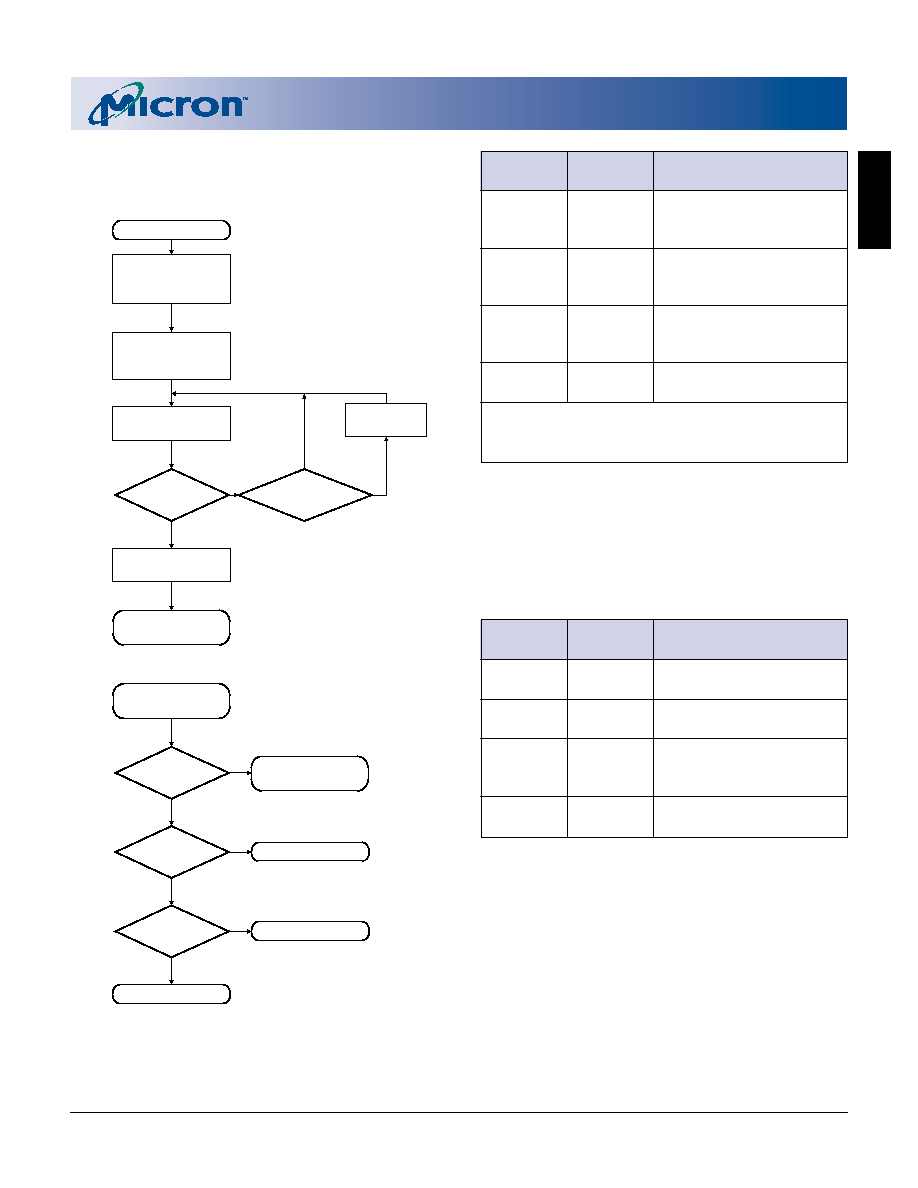
FLASH
24
4 Meg x 16 Asynchronous/Page Flash 512K x 16 SRAM Combo Memory
Micron Technology, Inc., reserves the right to change products or specifications without notice.
MT28C6428P20_3.p65 ≠ Rev. 3, Pub. 7/02
©2002, Micron Technology, Inc.
4 MEG x 16 ASYNCHRONOUS/PAGE FLASH
512K x 16 SRAM COMBO MEMORY
ADVANCE
YES
NO
Full Status Register
Check (optional)
NO
YES
ERASE
SUSPEND?
SR 7 = 1?
Start
BLOCK ERASE Passed
V
PP
Range Error
BLOCK ERASE Failed
FULL STATUS REGISTER CHECK FLOW
Read Status Register
Bits
ERASE
SUSPEND Loop
1
YES
NO
SR1 = 0?
YES
NO
YES
NO
BLOCK ERASE
Completed
Read Status Register
Bits
ERASE Attempted
on a Locked Block
SR3 = 0?
SR5 = 0?
Issue ERASE SETUP
Command and
Block Address
Issue BLOCK ERASE
CONFIRM Command
and Block Address
Figure 7
BLOCK ERASE Flowchart
NOTE: 1. Full status register check can be done after each block or after a sequence of blocks.
2. SR3 must be cleared before attempting additional PROGRAM/ERASE operations.
3. SR5 is cleared only by the CLEAR STATUS REGISTER command in cases where multiple blocks are erased before full
status is checked.
BUS
OPERATION COMMAND COMMENTS
WRITE
WRITE
Data = 20h
ERASE
Block Addr = Address
SETUP
within block to be erased
WRITE
ERASE
Data = D0h
Block Addr = Address
within block to be erased
READ
Status register data;
toggle OE# or CE# to
update status register.
Standby
Check SR7
1 = Ready, 0 = Busy
Repeat for subsequent blocks.
Write FFh after the last BLOCK ERASE operation to
reset the device to read array mode.
BUS
OPERATION COMMAND COMMENTS
Standby
Check SR1
1 = Detect locked block
Standby
Check SR3
2
1 = Detect F_V
PP
block
Standby
Check SR4 and SR5
1 = BLOCK ERASE
command error
Standby
Check SR5
3
1 = BLOCK ERASE error
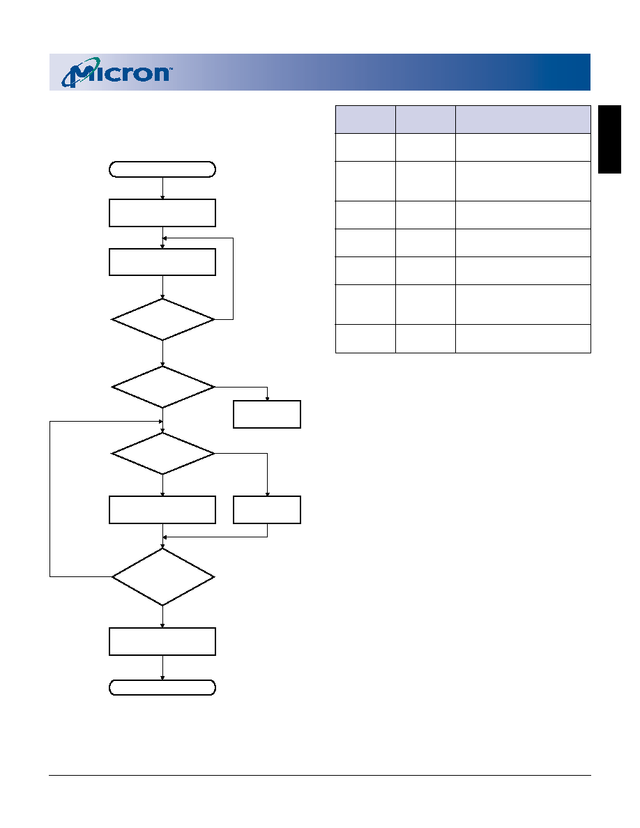
FLASH
25
4 Meg x 16 Asynchronous/Page Flash 512K x 16 SRAM Combo Memory
Micron Technology, Inc., reserves the right to change products or specifications without notice.
MT28C6428P20_3.p65 ≠ Rev. 3, Pub. 7/02
©2002, Micron Technology, Inc.
4 MEG x 16 ASYNCHRONOUS/PAGE FLASH
512K x 16 SRAM COMBO MEMORY
ADVANCE
READ
PROGRAM
Issue READ ARRAY
Command
PROGRAM
Loop
ERASE
Complete
READ or
PROGRAM?
YES
NO
Issue ERASE
RESUME Command
READ or
PROGRAM
Complete?
YES
NO
SR6 = 1?
Start
ERASE Continued
Read Status Register
Bits
Issue ERASE
SUSPEND Command
2
(Note 1)
YES
NO
SR7 = 1?
Figure 8
ERASE SUSPEND/ERASE RESUME
Flowchart
NOTE: 1. See Word Programming Flowchart for complete programming procedure.
2. See BLOCK ERASE Flowchart for complete erasure procedure.
BUS
OPERATION COMMAND COMMENTS
WRITE
ERASE
Data = B0h
SUSPEND
READ
Status register data;
toggle OE# or CE# to
update status register.
Standby
Check SR7
1 = Ready
Standby
Check SR6
1 = Suspended
WRITE
READ
Data = FFh
MEMORY
READ
Read data from block
other than that being
erased.
WRITE
ERASE
Data = D0h
RESUME

FLASH
26
4 Meg x 16 Asynchronous/Page Flash 512K x 16 SRAM Combo Memory
Micron Technology, Inc., reserves the right to change products or specifications without notice.
MT28C6428P20_3.p65 ≠ Rev. 3, Pub. 7/02
©2002, Micron Technology, Inc.
4 MEG x 16 ASYNCHRONOUS/PAGE FLASH
512K x 16 SRAM COMBO MEMORY
ADVANCE
Figure 9
CHECK BLOCK ERASE Flowchart
BUS
OPERATION COMMAND COMMENTS
WRITE
ERASE
Data = 20h
SETUP
Block Addr = Address
within block to be
checked
WRITE
CHECK
Data = D1
BLOCK
Block Addr = Address
ERASE
within block to be
CONFIRM
checked
READ
Status register data
Toggle OE# or CE# to
update status register
Standby
Check SR7 and SR5
Issue ERASE SETUP
Command and
Block Address
Error
Issue CHECK BLOCK
ERASE CONFIRM
Command
and Block Address
YES
Start
BLOCK ERASE
Complete
YES
NO
SR7 = 1?
NO
SR5 = 0?

FLASH
27
4 Meg x 16 Asynchronous/Page Flash 512K x 16 SRAM Combo Memory
Micron Technology, Inc., reserves the right to change products or specifications without notice.
MT28C6428P20_3.p65 ≠ Rev. 3, Pub. 7/02
©2002, Micron Technology, Inc.
4 MEG x 16 ASYNCHRONOUS/PAGE FLASH
512K x 16 SRAM COMBO MEMORY
ADVANCE
READ-WHILE-WRITE/ERASE
CONCURRENCY
It is possible for the device to read from one bank
while erasing/writing to another bank. Once a bank
enters the WRITE/ERASE operation, the other bank
automatically enters read array mode. For example,
during a READ CONCURRENCY operation, if a PRO-
GRAM/ERASE command is issued in bank a, then bank
a changes to the read status mode and bank b defaults
to the read array mode. The device reads from bank b if
the latched address resides in bank b (see Figure 10).
Similarly, if a PROGRAM/ERASE command is issued in
bank b, then bank b changes to read status mode and
bank a defaults to read array mode. When returning to
bank a, the device reads program/erase status if the
latched address resides in bank a.
A correct bank address must be specified to read
status register after returning from concurrent read in
the other bank.
When reading the CFI or the chip protection regis-
ter, concurrent operation is not allowed on the top boot
device. Concurrent READ of the CFI or the chip protec-
tion register is only allowed when a PROGRAM or ERASE
operation is performed on bank b on the bottom boot
device. For a bottom boot device, reading of the CFI
table or the chip protection register is only allowed if
bank b is in read array mode. For a top boot device,
reading of the CFI table or the chip protection register
is only allowed if bank a is in read array mode.
BLOCK LOCKING
The Flash memory of the MT28C6428P20 and
MT28C6428P18 devices provide a flexible locking
scheme which allows each block to be individually
locked or unlocked with no latency.
The devices offer two-level protection for the blocks.
The first level allows software-only control of block lock-
ing (for data which needs to be changed frequently),
while the second level requires hardware interaction
before locking can be changed (code which does not
require frequent updates).
Control signals F_WP#, DQ0, and DQ1 define the
state of a block; for example, state [001] means
F_WP# = 0, DQ0 = 0 and DQ1 = 1.
Table 9 defines all of the possible locking states.
NOTE: All blocks are software-locked upon comple-
tion of the power-up sequence.
Figure 10
READ-While-WRITE Concurrency
Bank a
1 - Erasing/writing to bank a
2 - Erasing in bank a can be
suspended, and a WRITE to
another block in bank a
can be initiated.
3 - After the WRITE in that block
is complete, an ERASE can
be resumed by writing an
ERASE RESUME command.
1 - Reading bank a
Bank b
1 - Reading from bank b
1 - Erasing/writing to bank b
2 - Erasing in bank b can be
suspended, and a WRITE to
another block in bank b
can be initiated.
3 - After the WRITE in that block
is complete, an ERASE can
be resumed by writing an
ERASE RESUME command.
LOCKED STATE
After a power-up sequence completion, or after a
reset sequence, all blocks are locked (states [001] or
[101]). This means full protection from alteration. Any
PROGRAM or ERASE operations attempted on a locked
block will return an error on bit SR1 of the status regis-
ter. The status of a locked block can be changed to
unlocked or lock down using the appropriate software
commands. Writing the lock command sequence, 60h
followed by 01h, can lock an unlocked block.
UNLOCKED STATE
Unlocked blocks (states [000], [100], [110]) can be
programmed or erased. All unlocked blocks return to
the locked state when the device is reset or powered
down. An unlocked block can be locked or locked down
using the appropriate software command sequence,
60h followed by D0h. (See Table 4.)
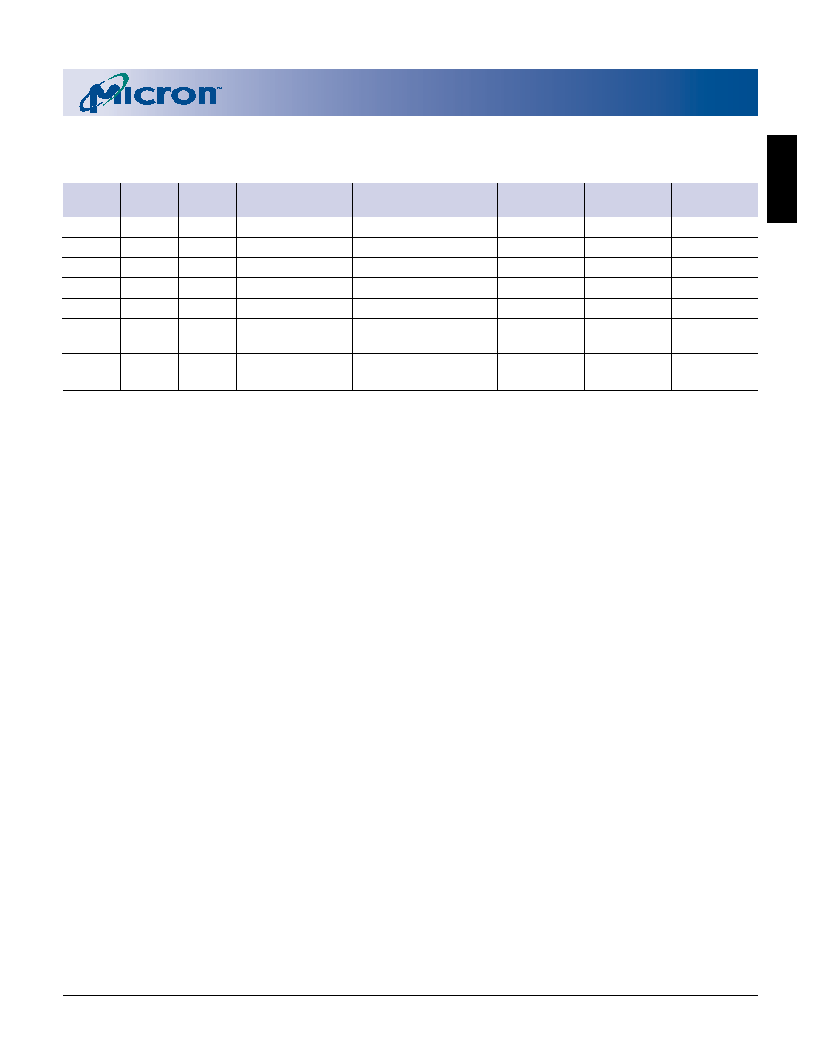
FLASH
28
4 Meg x 16 Asynchronous/Page Flash 512K x 16 SRAM Combo Memory
Micron Technology, Inc., reserves the right to change products or specifications without notice.
MT28C6428P20_3.p65 ≠ Rev. 3, Pub. 7/02
©2002, Micron Technology, Inc.
4 MEG x 16 ASYNCHRONOUS/PAGE FLASH
512K x 16 SRAM COMBO MEMORY
ADVANCE
LOCKED DOWN STATE
Blocks locked down (state [011]) are protected from
PROGRAM and ERASE operations, but their protection
status cannot be changed using software commands
alone. A locked or unlocked block can be locked down
by writing the lock down command sequence, 60h fol-
lowed by 2Fh. Locked down blocks revert to the locked
state when the device is reset or powered down.
The LOCK DOWN function is dependent on the
F_WP# input. When F_WP# = 0, blocks in lock down
[011] are protected from program, erase, and lock sta-
tus changes. When F_WP# = 1, the LOCK DOWN func-
tion is disabled ([111]) and locked down blocks can be
individually unlocked by a software command to the
[110] state, where they can be erased and programmed.
These blocks can then be relocked [111] and unlocked
[110], as desired, as long as F_WP# remains HIGH.
When F_WP# goes LOW, blocks that were previously
locked down return to the lock down state [011] regard-
less of any changes made while F_WP# was HIGH. De-
vice reset or power-down resets all locks, including
those in lock down, to the locked state (see Table 10).
READING A BLOCK'S LOCK STATUS
The lock status of every block can be read in the
read device identification mode. To enter this mode,
write 90h to the bank containing address 00h. Subse-
quent READs at block address +00002h will output the
lock status of that block. The lowest two outputs, DQ0
and DQ1, represent the lock status. DQ0 indicates the
block lock/unlock status and is set by the LOCK com-
mand and cleared by the UNLOCK command. It is also
automatically set when entering lock down. DQ1 indi-
cates lock down status and is set by the LOCK DOWN
command. It can only be cleared by reset or power-
down, not by software. Table 9 shows the block locking
state transition scheme. The READ ARRAY command,
FFh, must be issued to the bank containing address
00h prior to issuing other commands.
LOCKING OPERATIONS DURING ERASE
SUSPEND
Changes to block lock status can be performed dur-
ing an ERASE SUSPEND by using the standard locking
command sequences to unlock, lock, or lock down. This
is useful in the case when another block needs to be
updated while an ERASE operation is in progress.
To change block locking during an ERASE opera-
tion, first write the ERASE SUSPEND command (B0h),
then check the status register until it indicates that the
ERASE operation has been suspended. Next, write the
desired lock command sequence to block lock, and the
lock status will be changed. After completing any de-
sired LOCK, READ, or PROGRAM operations, resume
the ERASE operation with the ERASE RESUME com-
mand (D0h).
If a block is locked or locked down during an ERASE
SUSPEND on the same block, the locking status bits
are changed immediately. When the ERASE is resumed,
the ERASE operation completes.
A locking operation cannot be performed during a
PROGRAM SUSPEND.
STATUS REGISTER ERROR CHECKING
Using nested locking or program command se-
quences during ERASE SUSPEND can introduce ambi-
guity into status register results.
Following protection configuration setup (60h), an
invalid command produces a lock command error (SR4
and SR5 are set to "1") in the status register. If a lock
command error occurs during an ERASE SUSPEND,
SR4 and SR5 are set to "1" and remain at "1" after the
ERASE SUSPEND command is issued. When the ERASE
Table 9
Block Locking State Transition
ERASE/PROGRAM
LOCK
F_WP#
DQ1
DQ0
NAME
ALLOWED
LOCK
UNLOCK
DOWN
0
0
0
Unlocked
Yes
To [001]
≠
To [011]
0
0
1
Locked (Default)
No
≠
To [000]
To [011]
0
1
1
Lock Down
No
≠
≠
≠
1
0
0
Unlocked
Yes
To [101]
≠
To [111]
1
0
1
Locked
No
≠
To [100]
To [111]
1
1
0
Lock Down
Yes
To [111]
≠
To [111]
Disabled
1
1
1
Lock Down
No
≠
To [110]
≠
Disabled

FLASH
29
4 Meg x 16 Asynchronous/Page Flash 512K x 16 SRAM Combo Memory
Micron Technology, Inc., reserves the right to change products or specifications without notice.
MT28C6428P20_3.p65 ≠ Rev. 3, Pub. 7/02
©2002, Micron Technology, Inc.
4 MEG x 16 ASYNCHRONOUS/PAGE FLASH
512K x 16 SRAM COMBO MEMORY
ADVANCE
is complete, any possible error during the ERASE can-
not be detected via the status register because of the
previous locking command error.
A similar situation happens if an error occurs during
a program operation error nested within an ERASE
SUSPEND.
CHIP PROTECTION REGISTER
A 128-bit chip protection register can be used to
fullfill the security considerations in the system (pre-
venting device substitution).
The 128-bit security area is divided into two 64-bit
segments. The first 64 bits are programmed at the
manufacturing site with a unique 64-bit number. The
other segment is left blank for customers to program as
desired. (See Figure 12).
READING THE CHIP PROTECTION REGISTER
The chip protection register is read in the device
identification mode. To enter this mode, load the 90h
command the bank containing address 00h. Once in
this mode, READ cycles from addresses shown in Table
10 retrieve the specified information. To return to the
read array mode, write the READ ARRAY command
(FFh). The READ ARRAY command, FFh, must be is-
sued to the bank containing address 00h prior to issu-
ing other commands.
PAGE READ MODE
The initial portion of the page mode cycle is the
same as the asynchronous access cycle. Holding CE#
LOW and toggling addresses A0≠A2 allows random ac-
cess of other words in the page.
The page size can be customized at the factory to
four or eight words as required; but if no specification is
made, the normal size is four words.
ASYNCHRONOUS READ CYCLE
When accessing addresses in a random order or
when switching between pages, the access time is given
by
t
AA.
When F_CE# and F_OE# are LOW, the data is placed
on the data bus and the processor can read the data.
Figure 12
Protection Register Memory Map
4 Words
Factory-Programmed
4 Words
User-Programmed
PR Lock
0
88h
85h
84h
81h
80h
ITEM
ADDRESS
2
DATA
Manufacturer Code (x16)
00000h
002Ch
Device Code
00001h
∑
Top boot configuration
44B6h
∑
Bottom boot configuration
44B7h
Block Lock Configuration
XX002h
Lock
∑
Block is unlocked
DQ0 = 0
∑
Block is locked
DQ0 = 1
∑
Block is locked down
DQ1 = 1
Chip Protection Register Lock
80h
PR Lock
Chip Protection Register 1
81h≠84h
Factory Data
Chip Protection Register 2
85h≠88h
User Data
NOTE: 1. Other locations within the configuration address space are reserved by
Micron for future use.
2. "XX" specifies the block address of lock configuration.
Table 10
Chip Configuration Addressing
1
FLASH
30
4 Meg x 16 Asynchronous/Page Flash 512K x 16 SRAM Combo Memory
Micron Technology, Inc., reserves the right to change products or specifications without notice.
MT28C6428P20_3.p65 ≠ Rev. 3, Pub. 7/02
©2002, Micron Technology, Inc.
4 MEG x 16 ASYNCHRONOUS/PAGE FLASH
512K x 16 SRAM COMBO MEMORY
ADVANCE
STANDBY MODE
I
CC
supply current is reduced by applying a logic
HIGH level on F_CE# and F_RP# to enter the standby
mode. In the standby mode, the outputs are placed in
High-Z. Applying a CMOS logic HIGH level on F_CE#
and F_RP# reduces the current to I
CC
3
(MAX). If the
device is deselected during an ERASE operation or dur-
ing programming, the device continues to draw cur-
rent until the operation is complete.
AUTOMATIC POWER SAVE (APS) MODE
Substantial power savings are realized during peri-
ods when the Flash array is not being read and the
device is in the active mode. During this time the de-
vice switches to the automatic power save (APS) mode.
When the device switches to this mode, I
CC
is reduced
to a level comparable to I
CC
3
. Further power savings can
be realized by applying a logic HIGH level on CE# to
place the device in standby mode. The low level of
power is maintained until another operation is initi-
ated. In this mode, the I/Os retain the data from the
last memory address read until a new address is read.
This mode is entered automatically if no addresses or
control signals toggle.
DEEP POWER-DOWN MODE
By issuing an ENABLE DEEP POWER-DOWN com-
mand (see Table 3) it is possible to enable the DEEP
POWER-DOWN function. In this configuration, apply-
ing a logic LOW to RST# reduces the current to I
CC
10
, and
resets all the internal registers with the exception of the
individual block protection status. To exit this mode, a
wait time of 100µs (
t
RWHDP) must elapse after a logic
HIGH is applied to RST#. During the wait time, the
device performs a full power-up sequence, and the
power consumption may exceed the standby current
limits.
F_V
PP
/F_V
CC
PROGRAM AND ERASE
VOLTAGES
The Flash memory devices provide in-system
programming and erase with F_V
PP
in the 0.9V≠2.2V
range. In addition to the flexible block locking, the F_V
PP
programming voltage can be held LOW for absolute
hardware write protection of all blocks in the Flash de-
vice. When F_V
PP
is below V
PPLK
, any PROGRAM or ERASE
operation results in an error, prompting the corre-
sponding status register bit (SR3) to be set.
A factory option provides in-system programming
and erase with F_V
PP
in the 0.0V≠2.2V range.
F_V
PP
at 12V ±5% (F_V
PP
2
) is supported for a maxi-
mum of 100 cycles and 10 cumulative hours. The de-
vice can withstand 100,000 WRITE/ERASE operations
when F_V
PP
= F_V
CC
.
During WRITE and ERASE operations, the WSM
monitors the F_V
PP
voltage level. WRITE/ERASE opera-
tions are allowed only when F_V
PP
is within the ranges
specified in Table 11.
When F_V
CC
is below V
LKO
or F_V
PP
is below
VPPLK
, any
WRITE/ERASE operation is prevented.
DEVICE RESET
To correctly reset the device, the RST# signal must
be asserted (RST# = V
IL
) for a minimum of
t
RP. After
reset, the device can be accessed for a READ operation
with a delayed access time of
t
RWH from the rising edge
of RST#. The circuitry used for generating the RST#
signal needs to be common with the rest of the system
reset to ensure that correct system initialization occurs.
Please refer to the timing diagram for further details.
POWER-UP SEQUENCE
The following power-up sequence is recommended
to properly initialize internal chip operations:
∑ At power-up, RST# should be kept at V
IL
for 2µs
after F_V
CC
reaches F_V
CC
(MIN).
∑ V
CC
Q should not come up before F_V
CC
.
∑ F_V
PP
should be kept at V
IL
to maximize data
integrity.
When the power-up sequence is completed, RST#
should be brought to V
IH
. To ensure proper power-up,
the rise time of RST# (10%≠90%) should be < 10µs.
Table 11
F_V
PP
Ranges (V)
DEVICE
MIN
MAX
In-System
0.9
2.2
In-Factory
11.4
12.6

FLASH
31
4 Meg x 16 Asynchronous/Page Flash 512K x 16 SRAM Combo Memory
Micron Technology, Inc., reserves the right to change products or specifications without notice.
MT28C6428P20_3.p65 ≠ Rev. 3, Pub. 7/02
©2002, Micron Technology, Inc.
4 MEG x 16 ASYNCHRONOUS/PAGE FLASH
512K x 16 SRAM COMBO MEMORY
ADVANCE
ABSOLUTE MAXIMUM RATINGS*
Voltage to Any Ball Except F_V
CC
and F_V
PP
with Respect to V
SS
............................ -0.5V to +2.45V
F_V
PP
Voltage (for BLOCK ERASE and PROGRAM
with Respect to V
SS
) ....................... -0.5V to +13.5V**
F_V
CC
and V
CC
Q Supply Voltage
with Respect to V
SS
............................ -0.3V to +2.45V
Output Short Circuit Current ............................... 100mA
Operating Temperature Range .............. -40
o
C to +85
o
C
Storage Temperature Range ................. -55
o
C to +125
o
C
Soldering Cycle ........................................... 260
o
C for 10s
*Stresses greater than those listed under "Absolute
Maximum Ratings" may cause permanent damage to
the device. This is a stress rating only and functional
operation of the device at these or any other conditions
above those indicated in the operational sections of
this specification is not implied. Exposure to absolute
maximum rating conditions for extended periods may
affect reliability.
**Maximum DC voltage on F_V
PP
may overshoot to
+13.5V for periods <20ns.
RECOMMENDED OPERATING CONDITIONS
(-40∫C
T
A
+85∫C)
PARAMETER
SYMBOL
MIN
MAX
UNITS
NOTES
V
CC
supply voltage (MT28C6428P18)
F_V
CC
, S_V
CC
1.70
1.90
V
V
CC
supply voltage (MT28C6428P20)
F_V
CC
, S_V
CC
1.80
2.20
V
I/O supply voltage (MT28C6428P18)
V
CC
Q
1.70
1.90
V
I/O supply voltage (MT28C6428P20)
V
CC
Q
1.80
2.20
V
F_V
PP
voltage (when used as logic control)
F_V
PP
1
0.9
2.2
V
F_V
PP
in-factory programming voltage
F_V
PP
2
11.4
12.6
V
Data retention supply voltage
S_V
DR
1.0
≠
V
Block erase cycling (F_V
PP
1
)
F_V
PP
=
F_V
PP
1
F_V
PP
1
≠
100,000
Cycles
F_V
PP
=
F_V
PP
2
F_V
PP
2
≠
100
Cycles
1
FLASH ELECTRICAL SPECIFICATIONS
NOTE: 1. F_V
PP
= F_V
PP
2
is a maximum of 10 cumulative hours.
Figure 14
Output Load Circuit
I/O
14.5K
30pF
V
CC
V
SS
14.5K
Output
Test Points
Input
V
CC
V
SS
AC test inputs are driven at V
CC
for a logic 1 and V
SS
for a logic 0. Input timing begins at V
CC
/2,
and output timing ends
at V
CC
Q/2. Input rise and fall times (10% to 90%) < 5ns.
V
CC
Q/2
V
CC
/2
Figure 13
AC Input/Output Reference Waveform
FLASH
32
4 Meg x 16 Asynchronous/Page Flash 512K x 16 SRAM Combo Memory
Micron Technology, Inc., reserves the right to change products or specifications without notice.
MT28C6428P20_3.p65 ≠ Rev. 3, Pub. 7/02
©2002, Micron Technology, Inc.
4 MEG x 16 ASYNCHRONOUS/PAGE FLASH
512K x 16 SRAM COMBO MEMORY
ADVANCE
COMBINED DC CHARACTERISTICS
1
F_V
CC
/V
CC
Q = 1.70V≠1.90V
or 1.80V≠2.20V
DESCRIPTION
CONDITIONS
SYMBOL
MIN
TYP
MAX
UNITS NOTES
Input Low Voltage
V
IL
0.0
≠
0.4
V
2
Input High Voltage
V
IH
V
CC
Q - 0.4
≠
V
CC
Q
V
2
Output Low Voltage
V
OL
≠
≠
0.10
V
I
OL
= 100µA (Flash)
Output Low Voltage
V
OL
≠
≠
0.3
V
I
OL
= 100µA (SRAM)
Output High Voltage
V
OH
V
CC
Q - 0.1
≠
≠
V
I
OH
= -100µA (Flash)
Output High Voltage
V
OH
V
CC
Q - 0.3
≠
≠
V
I
OH
= -100µA (SRAM)
F_V
PP
Lockout Voltage
V
PPLK
≠
≠
0.4
V
F_V
PP
During PROGRAM/ERASE
F_V
PP
1
0.9
≠
2.2
V
Operations
F_V
PP
2
11.4
≠
12.6
V
3
F_V
CC
Program/Erase Lock Voltage
V
LKO
1.0
≠
≠
V
Input Leakage Current
I
L
≠
≠
1.0
µA
Output Leakage Current
I
OZ
≠
≠
1.0
µA
F_V
CC
Read Current
I
CC
1
4, 5
Asynchronous Random Read,
≠
≠
15
mA
100ns cycle
Asynchronous Page Read,
I
CC
2
≠
≠
5
mA
4, 5
100ns/35ns cycle
F_V
CC
plus S_V
CC
Standby Current
I
CC
3
≠
25
70
µA
F_V
CC
Program Current
I
CC
4
≠
≠
55
mA
F_V
CC
Erase Current
I
CC
5
≠
18
45
mA
F_V
CC
Erase Suspend Current
I
CC
6
≠
6
70
µA
6
F_V
CC
Program Suspend Current
I
CC
7
≠
6
70
µA
6
Read-While-Write Current
I
CC
8
≠
≠
80
mA
NOTE: 1. All currents are in RMS unless otherwise noted.
2. V
IL
may decrease to -0.4V and V
IH
may increase to V
CC
Q + 0.3V for durations not to exceed 20ns.
3. 12V F_V
PP
is supported for a maximum of 100 cycles and may be connected for up to 10 cumulative hours.
4. APS mode reduces I
CC
to approximately I
CC
3
levels.
5. Test conditions: Vcc = V
CC
(MAX), CE# = V
IL
, OE# = V
IH
. All other inputs = V
IH
or V
IL
.
6. I
CC
6
and I
CC
7
values are valid when the device is deselected. Any read operation performed while in suspend mode will
add a current draw of I
CC
1
or I
CC
2
.
(continued on next page)
FLASH
33
4 Meg x 16 Asynchronous/Page Flash 512K x 16 SRAM Combo Memory
Micron Technology, Inc., reserves the right to change products or specifications without notice.
MT28C6428P20_3.p65 ≠ Rev. 3, Pub. 7/02
©2002, Micron Technology, Inc.
4 MEG x 16 ASYNCHRONOUS/PAGE FLASH
512K x 16 SRAM COMBO MEMORY
ADVANCE
COMBINED DC CHARACTERISTICS
1
(continued)
F_V
CC
/V
CC
Q = 1.70V≠1.90V
or 1.80V≠2.20V
DESCRIPTION
CONDITIONS
SYMBOL
MIN
TYP
MAX
UNITS NOTES
S_V
CC
Read/Write Operating
V
IN
= V
IH
or V
IL
I
CC
9
≠
12
15
mA
Supply Current ≠ Random
chip enabled,
Access Mode
I
OL
= 0
S_V
CC
Read/Write Operating
V
IN
= V
IH
or V
IL
I
CC
10
≠
2
3
mA
Supply Current ≠ Page Access
chip enabled,
Mode
I
OL
= 0
Deep Power-Down Current
I
CC
11
≠
35
45
µA
F_V
PP
Current
F_V
PP
F_V
CC
I
PP
1
0.5
≠
1
µA
(Read, Standby Erase Suspend,
F_V
PP
F_V
CC
50
≠
200
µA
Program Suspend)
NOTE: 1. All currents are in RMS unless otherwise noted.
2. V
IL
may decrease to -0.4V and V
IH
may increase to V
CC
Q + 0.3V for durations not to exceed 20ns.
3. 12V F_V
PP
is supported for a maximum of 100 cycles and may be connected for up to 10 cumulative hours.
4. APS mode reduces I
CC
to approximately I
CC
3
levels.
5. Test conditions: Vcc = V
CC
(MAX), CE# = V
IL
, OE# = V
IH
. All other inputs = V
IH
or V
IL
.
6. I
CC
6
and I
CC
7
values are valid when the device is deselected. Any read operation performed while in suspend mode will
add a current draw of I
CC
1
or I
CC
2
.

FLASH
34
4 Meg x 16 Asynchronous/Page Flash 512K x 16 SRAM Combo Memory
Micron Technology, Inc., reserves the right to change products or specifications without notice.
MT28C6428P20_3.p65 ≠ Rev. 3, Pub. 7/02
©2002, Micron Technology, Inc.
4 MEG x 16 ASYNCHRONOUS/PAGE FLASH
512K x 16 SRAM COMBO MEMORY
ADVANCE
CAPACITANCE
(T
A
= +25∫C; f = 1 MHz)
PARAMETER/CONDITION
SYMBOL
TYP
MAX
UNITS
Input Capacitance
C
7
12
p F
Output Capacitance
C
OUT
13
15
p F
FLASH READ CYCLE TIMING REQUIREMENTS
-80
-85
F_V
CC
= 1.80V
≠
2.20V
F_V
CC
= 1.70V
≠
1.90V
PARAMETER
SYMBOL
MIN
MAX
MIN
MAX
UNITS
Address to output delay
t
AA
80
85
ns
F_CE# LOW to output delay
t
ACE
80
85
ns
Page address access
t
APA
30
35
ns
F_OE# LOW to output delay
t
AOE
25
30
ns
F_RP# HIGH to output delay
t
RWH
200
250
ns
CE# or OE# HIGH to output High-Z
t
OD
20
25
ns
Output hold from address, CE# or OE# change
t
OH
0
0
ns
READ cycle time
t
RC
80
85
ns
RST# deep power-down
t
RWHOP
100
100
µs
FLASH
35
4 Meg x 16 Asynchronous/Page Flash 512K x 16 SRAM Combo Memory
Micron Technology, Inc., reserves the right to change products or specifications without notice.
MT28C6428P20_3.p65 ≠ Rev. 3, Pub. 7/02
©2002, Micron Technology, Inc.
4 MEG x 16 ASYNCHRONOUS/PAGE FLASH
512K x 16 SRAM COMBO MEMORY
ADVANCE
FLASH WRITE CYCLE TIMING REQUIREMENTS
-80
-85
F_V
CC
= 1.80V
≠
2.20V
F_V
CC
= 1.70V
≠
1.90V
PARAMETER
SYMBOL
MIN
MAX
MIN
MAX
UNITS
Reset HIGH recovery to F_WE# going LOW
t
RS
150
150
ns
F_CE# setup to F_WE# going LOW
t
CS
0
0
ns
Write pulse width
t
WP
50
70
ns
Data setup to F_WE# going HIGH
t
DS
50
70
ns
Address setup to F_WE# going HIGH
t
AS
50
70
ns
F_CE# hold from F_WE# HIGH
t
CH
0
0
ns
Data hold from F_WE# HIGH
t
DH
0
0
ns
Address hold from F_WE# HIGH
t
AH
0
0
ns
Write pulse width HIGH
t
WPH
30
30
ns
F_WP# setup to F_WE# going HIGH
t
RHS
0
0
ns
F_V
PP
setup to F_WE# going HIGH
t
VPS
200
200
ns
Write recovery before READ
t
WOS
50
50
ns
Write recovery before READ in opposite bank
t
WOA
0
0
ns
F_WP# hold from valid SRD
t
RHH
0
0
ns
F_V
PP
hold from valid SRD
t
VPPH
0
0
ns
F_WE# HIGH to data valid
t
WB
t
AA + 50
t
AA + 50
ns
FLASH ERASE AND PROGRAM CYCLE TIMING REQUIREMENTS
-80/-85
PARAMETER
TYP
MAX
UNITS
4KW parameter block program time
40
800
ms
32KW parameter block program time
320
6,400
ms
Word program time
8
10,000
µs
4KW parameter block erase time
0.3
6
s
32KW parameter block erase time
0.5
6
s
Program suspend latency
5
10
µs
Erase suspend latency
5
20
µs
Chip programming time
20
S

FLASH
36
4 Meg x 16 Asynchronous/Page Flash 512K x 16 SRAM Combo Memory
Micron Technology, Inc., reserves the right to change products or specifications without notice.
MT28C6428P20_3.p65 ≠ Rev. 3, Pub. 7/02
©2002, Micron Technology, Inc.
4 MEG x 16 ASYNCHRONOUS/PAGE FLASH
512K x 16 SRAM COMBO MEMORY
ADVANCE
TWO-CYCLE PROGRAMMING/ERASE OPERATION
VALID ADDRESS
VALID ADDRESS
VALID ADDRESS
UNDEFINED
t
CH
t
DH
t
RHS
t
DS
A0≠A21
F_OE#
F_CE#
F_WE#
F_V
PP
F_RP#
F_WP#
V
IH
V
IH
V
IL
V
IL
V
IH
V
IL
V
IH
V
IL
V
IH
V
I L
V
IH
V
IL
V
IPPLK
V
IL
V
IPPH
t
AS
t
AH
t
WPH
t
RS
t
WP
t
WOS
t
CS
t
WB
CMD
CMD/
DATA
DQ0≠DQ15
V
OH
V
OL
t
RHH
t
VPS
t
VPPH
STATUS
High-Z
NOTE: 1. The WRITE cycles for the WORD PROGRAMMING command are followed by a READ ARRAY DATA cycle.
-80
-85
F_V
CC
= 1.80V≠2.20V
F_V
CC
= 1.70V≠1.90V
SYMBOL
MIN
MAX
MIN
MAX
UNITS
WRITE TIMING PARAMETERS
-80
-85
F_V
CC
= 1.80V≠2.20V
F_V
CC
= 1.70V≠1.90V
SYMBOL
MIN
MAX
MIN
MAX
UNITS
t
RS
150
150
ns
t
CS
0
0
ns
t
WP
50
70
ns
t
DS
50
70
ns
t
AS
50
70
ns
t
CH
0
0
ns
t
DH
0
0
ns
t
AH
0
0
ns
t
RHS
0
0
ns
t
VPS
200
200
ns
t
WOS
50
50
ns
t
RHH
0
0
ns
t
VPPH
0
0
ns
t
WB
t
AA + 50
t
AA + 50
ns
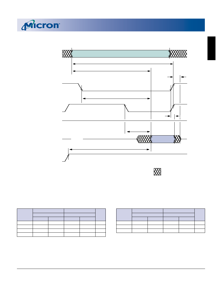
FLASH
37
4 Meg x 16 Asynchronous/Page Flash 512K x 16 SRAM Combo Memory
Micron Technology, Inc., reserves the right to change products or specifications without notice.
MT28C6428P20_3.p65 ≠ Rev. 3, Pub. 7/02
©2002, Micron Technology, Inc.
4 MEG x 16 ASYNCHRONOUS/PAGE FLASH
512K x 16 SRAM COMBO MEMORY
ADVANCE
SINGLE ASYNCHRONOUS READ OPERATION
VALID ADDRESS
UNDEFINED
t
OD
t
AA
t
ACE
t
OH
A0≠A21
F_OE#
F_CE#
F_WE#
V
IH
V
IL
V
IH
V
IL
V
IH
V
IL
V
IH
V
IL
V
IH
V
IL
t
RC
t
RWH
DQ0≠DQ15
F_RP#
V
OH
V
OL
VALID OUTPUT
High-Z
t
AOE
-80
-85
F_V
CC
= 1.80V≠2.20V
F_V
CC
= 1.70V≠1.90V
SYMBOL
MIN
MAX
MIN
MAX
UNITS
READ TIMING PARAMETERS
-80
-85
F_V
CC
= 1.80V≠2.20V
F_V
CC
= 1.70V≠1.90V
SYMBOL
MIN
MAX
MIN
MAX
UNITS
t
AA
80
85
ns
t
ACE
80
85
ns
t
AOE
25
30
ns
t
RWH
200
250
ns
t
OD
20
25
ns
t
OH
0
0
ns
t
RC
80
85
ns
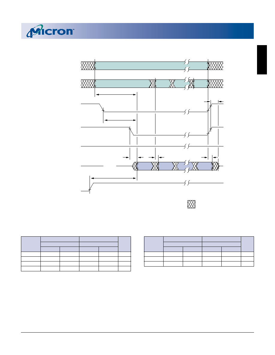
FLASH
38
4 Meg x 16 Asynchronous/Page Flash 512K x 16 SRAM Combo Memory
Micron Technology, Inc., reserves the right to change products or specifications without notice.
MT28C6428P20_3.p65 ≠ Rev. 3, Pub. 7/02
©2002, Micron Technology, Inc.
4 MEG x 16 ASYNCHRONOUS/PAGE FLASH
512K x 16 SRAM COMBO MEMORY
ADVANCE
ASYNCHRONOUS PAGE MODE READ OPERATION
VALID ADDRESS
VALID
ADDRESS
VALID
ADDRESS
VALID
ADDRESS
VALID
OUTPUT
VALID
OUTPUT
VALID
OUTPUT
VALID
OUTPUT
UNDEFINED
t
OD
t
AA
t
ACE
t
OH
t
A
PA
t
AOE
t
RMH
A0≠A2
F_OE#
F_CE#
F_WE#
V
IH
V
IL
V
IH
V
IL
V
IH
V
IL
V
IH
V
IL
VALID ADDRESS
A3≠A21
V
IH
V
IL
F_RP#
V
IH
V
IL
DQ0≠DQ15
V
OH
V
OL
High-Z
-80
-85
F_V
CC
= 1.80V≠2.20V
F_V
CC
= 1.70V≠1.90V
SYMBOL
MIN
MAX
MIN
MAX
UNITS
READ TIMING PARAMETERS
-80
-85
F_V
CC
= 1.80V≠2.20V
F_V
CC
= 1.70V≠1.90V
SYMBOL
MIN
MAX
MIN
MAX
UNITS
t
AA
80
85
ns
t
ACE
80
85
ns
t
APA
30
35
ns
t
AOE
25
30
ns
t
RWH
200
250
ns
t
OD
20
25
ns
t
OH
0
0
ns
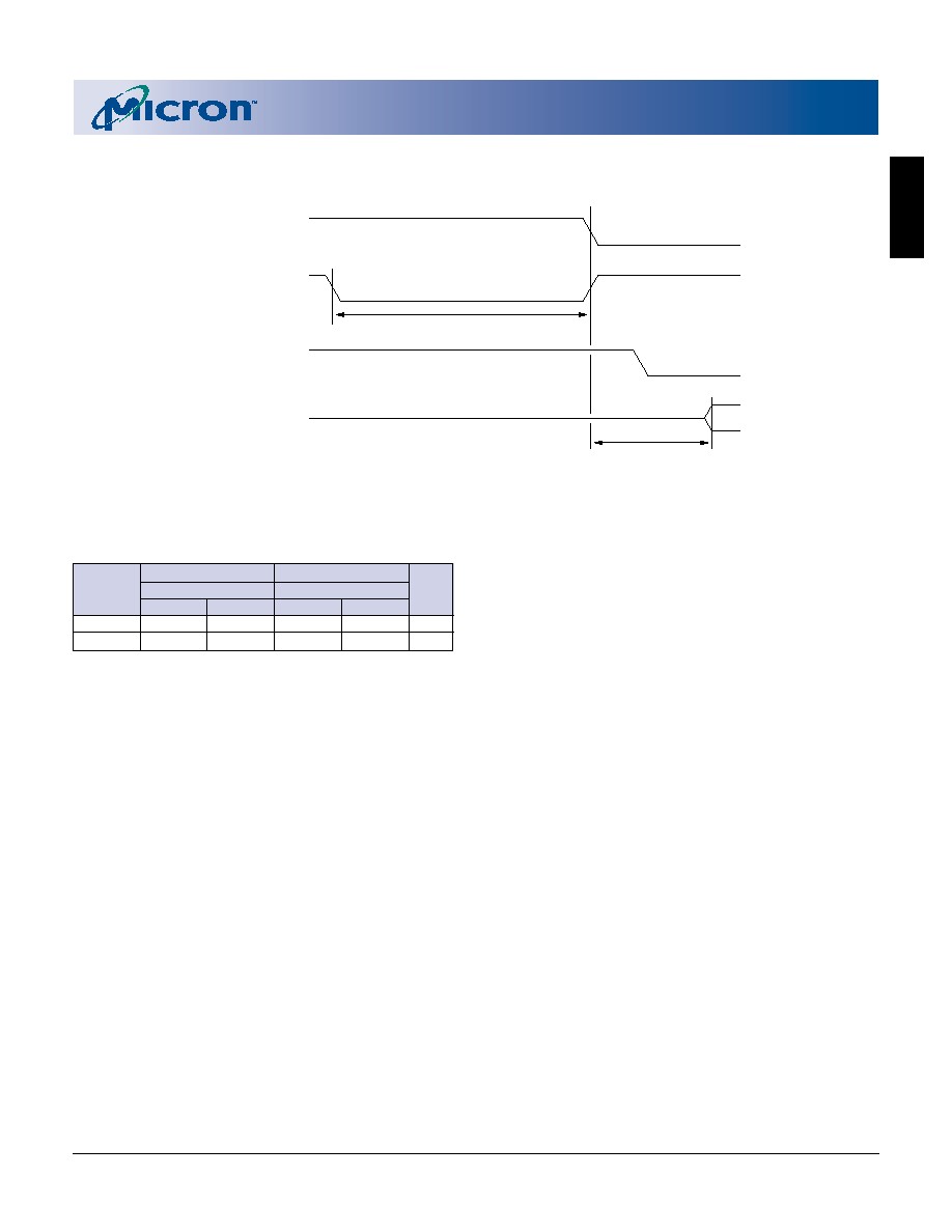
FLASH
39
4 Meg x 16 Asynchronous/Page Flash 512K x 16 SRAM Combo Memory
Micron Technology, Inc., reserves the right to change products or specifications without notice.
MT28C6428P20_3.p65 ≠ Rev. 3, Pub. 7/02
©2002, Micron Technology, Inc.
4 MEG x 16 ASYNCHRONOUS/PAGE FLASH
512K x 16 SRAM COMBO MEMORY
ADVANCE
RESET OPERATION
F_OE#
DQ0≠DQ15
V
IH
V
IL
F_RST#
V
IH
V
IL
F_CE#
V
IH
V
IL
V
OH
V
OL
t
RWH
t
RP
READ TIMING PARAMETERS
-80
-85
F_V
CC
= 1.80V≠2.20V
F_V
CC
= 1.70V≠1.90V
SYMBOL
MIN
MAX
MIN
MAX
UNITS
t
RWH
200
250
ns
t
RP
100
100
ns
FLASH
40
4 Meg x 16 Asynchronous/Page Flash 512K x 16 SRAM Combo Memory
Micron Technology, Inc., reserves the right to change products or specifications without notice.
MT28C6428P20_3.p65 ≠ Rev. 3, Pub. 7/02
©2002, Micron Technology, Inc.
4 MEG x 16 ASYNCHRONOUS/PAGE FLASH
512K x 16 SRAM COMBO MEMORY
ADVANCE
Table 12
CFI
OFFSET
DATA
DESCRIPTION
00
2Ch
Manufacturer code
01
B6h
Top boot block device code
B7h
Bottom boot block device code
02≠0F
reserved
Reserved
10, 11
0051,0052
"QR"
12
0059
"Y"
13, 14
0003, 0000
Primary OEM command set
15, 16
0039, 0000
Address for primary extended table
17, 18
0000, 0000
Alternate OEM command set
19, 1A
0000, 0000
Address for OEM extended table
1B
0017
F_V
CC
MIN for Erase/Write; Bit7≠Bit4 Volts in BCD; Bit3≠Bit0 100mV in BCD
1C
0022
F_V
CC
MAX for Erase/Write; Bit7≠Bit4 Volts in BCD; Bit3≠Bit0 100mV in BCD
1D
00B4
F_V
PP
MIN for Erase/Write; Bit7≠Bit4 Volts in Hex; Bit3≠Bit0 100mV in BCD
1E
00C6
F_V
PP
MAX for Erase/Write; Bit7≠Bit4 Volts in Hex; Bit3≠Bit0 100mV in BCD, 0000 = F_V
PP
ball
1F
0003
Typical timeout for single byte/word program, 2
n
µs, 0000 = not supported
20
0000
Typical timeout for maximum size multiple byte/word program, 2
n
µs, 0000 = not
supported
21
0009
Typical timeout for individual block erase, 2
n
ms, 0000 = not supported
22
0000
Typical timeout for full chip erase, 2
n
ms, 0000 = not supported
23
000C
Maximum timeout for single byte/word program, 2
n
µs, 0000 = not supported
24
0000
Maximum timeout for maximum size multiple byte/word program, 2
n
µs, 0000 = not
supported
25
0003
Maximum timeout for individual block erase, 2
n
ms, 0000 = not supported
26
0000
Maximum timeout for full chip erase, 2
n
ms, 0000 = not supported
27
0017
Device size, 2
n
bytes
28
0001
Bus interface x8 = 0, x16 = 1, x8/x16 = 2
29
0000
Flash device interface description 0000 = async
2A, 2B
0000, 0000
Maximum number of bytes in multibyte program or page, 2
n
2C
0003
Number of erase block regions within device (4K words and 32K words)
2D, 2E
5F00, 0001
Top boot block device erase block region information 1, 8 blocks ...
0007, 0000
Bottom boot block device erase block region information 1, 8 blocks ...
2F, 30
0000, 0001
Erase block region information 1, 8 blocks ...
0020, 0000
...of 8KB
31, 32
000E, 0000
15 blocks of ....
33, 34
0000, 0001
......64KB
35, 36
0007, 0000
Top boot block device ......96KB blocks of
5F00, 0001
Bottom boot block device ......96KB blocks of
(continued on the next page)
FLASH
41
4 Meg x 16 Asynchronous/Page Flash 512K x 16 SRAM Combo Memory
Micron Technology, Inc., reserves the right to change products or specifications without notice.
MT28C6428P20_3.p65 ≠ Rev. 3, Pub. 7/02
©2002, Micron Technology, Inc.
4 MEG x 16 ASYNCHRONOUS/PAGE FLASH
512K x 16 SRAM COMBO MEMORY
ADVANCE
Table 12
CFI (continued)
OFFSET
DATA
DESCRIPTION
37, 38
0020, 0000
Top boot block device......64KB
0000, 0001
Bottom boot block device......64KB
39, 3A
0050, 0052
"PR"
3B
0049
"I"
3C
0030
Major version number, ASCII
3D
0031
Minor version number, ASCII
3E
00E6
Optional Feature and Command Support
3F
0002
Bit 0 Chip erase supported no = 0
40
0000
Bit 1 Suspend erase supported = yes = 1
41
0000
Bit 2 Suspend program supported = yes = 1
Bit 3 Chip lock/unlock supported = no = 0
Bit 4 Queued erase supported = no = 0
Bit 5 Instant individual block locking supported = yes = 1
Bit 6 Protection bits supported = yes = 1
Bit 7 Page mode read supported = yes = 1
Bit 8 Synchronous read supported = yes = 1
Bit 9 Simultaneous operation supported = yes = 1
42
0001
Program supported after erase suspend = yes
43, 44
0003,0000
Bit 0 block lock status active = yes; Bit 1 block lock down active = yes
45
0018
F_V
CC
supply optimum; Bit7≠Bit4 Volts in BCD; Bit3≠Bit0 100mV in BCD
46
00C0
F_V
PP
supply optimum; Bit7≠Bit4 Volts in Hex; Bit3≠Bit0 100mV in BCD
47
0001
Number of protection register fields in JEDEC ID space
48, 49
0080, 0000
Lock bytes LOW address, lock bytes HIGH address
4A, 4B
0003, 0003
2
n
factory programmed bytes, 2
n
user programmable bytes
4C
0003
Background Operation
0000 = Not used
0001 = 4% block split
0002 = 12% block split
0003 = 25% block split
0004 = 50% block split
4D
0000
Burst Mode Type
0000 = No burst mode
00x1 = 4 words MAX
00x2 = 8 words MAX
00x3 = 16 words MAX
001x = Linear burst, and/or
002x = Interleaved burst, and/or
004x = Continuous burst
4E
0002
Page Mode Type
0000 = No page mode
0001 = 4-word page
0002 = 8-word page
0003 = 16-word page
0004 = 32-word page
4F
0008
SRAM density, 8Mb (512K x 16)
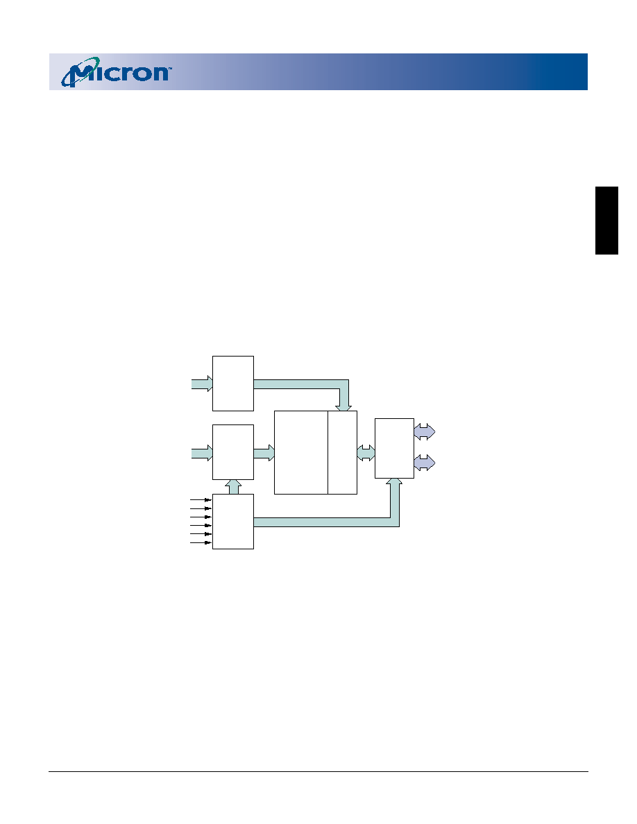
SRAM
42
4 Meg x 16 Asynchronous/Page Flash 512K x 16 SRAM Combo Memory
Micron Technology, Inc., reserves the right to change products or specifications without notice.
MT28C6428P20_3.p65 ≠ Rev. 3, Pub. 7/02
©2002, Micron Technology, Inc.
4 MEG x 16 ASYNCHRONOUS/PAGE FLASH
512K x 16 SRAM COMBO MEMORY
ADVANCE
SRAM OPERATING MODES
SRAM READ ARRAY
The operational state of the SRAM is determined by
S_CE1#, S_CE2, S_WE#, S_OE#, S_UB#, and S_LB#, as
indicated in the Truth Table. To perform an SRAM
READ operation, S_CE1#, and S_OE#, must be at V
IL
,
and S_CE2 and S_WE# must be at V
IH
. When in this
state, S_UB# and S_LB# control whether the lower byte
is read (S_UB# V
IH
, S_LB# V
IL
), the upper byte is read
(S_UB# V
IL
, S_LB# V
IH
), both upper and lower bytes are
read (S_UB# V
IL
, S_LB# V
IL
), or neither are read (S_UB#
V
IH
, S_LB# V
IH
) and the device is in a standby state.
While performing an SRAM READ operation, cur-
rent consumption may be reduced by reading within a
16-word page. This is done by holding S_CE1# and
SRAM FUNCTIONAL BLOCK DIAGRAM
DQ0≠DQ7
WORD
ADDRESS
DECODE
LOGIC
PAGE
ADDRESS
DECODE
LOGIC
CONTROL
LOGIC
16K-PAGE
x16 WORD
x16 BIT
RAM ARRAY
WORD
MUX
DQ8≠DQ15
INPUT/
OUTPUT
MUX
AND
BUFFERS
S_CE1#
A4≠A18
A0≠A3
S_OE#
S_UB#
S_LB#
S_CE2
S_WE#
S_OE# at V
IL
, S_WE# and S_CE2 at V
IH
, and toggling
addresses A0≠A3. S_UB# and S_LB# control the data
width as described above.
SRAM WRITE ARRAY
In order to perform an SRAM WRITE operation,
S_CE1# and S_WE# must be at V
IL
, and S_CE2 and
S_OE# must be at V
IH
. When in this state, S_UB# and
S_LB# control whether the lower byte is written (S_UB#
V
IH
, S_LB# V
IL
), the upper byte is written (S_UB# V
IL
,
S_LB# V
IH
), both upper and lower bytes are written
(S_UB# V
IL
, S_LB# V
IL
), or neither are written (S_UB#
V
IH
, S_LB# V
IH
) and the device is in a standby state.

SRAM
43
4 Meg x 16 Asynchronous/Page Flash 512K x 16 SRAM Combo Memory
Micron Technology, Inc., reserves the right to change products or specifications without notice.
MT28C6428P20_3.p65 ≠ Rev. 3, Pub. 7/02
©2002, Micron Technology, Inc.
4 MEG x 16 ASYNCHRONOUS/PAGE FLASH
512K x 16 SRAM COMBO MEMORY
ADVANCE
TIMING TEST CONDITIONS
Input pulse levels ........... 0.1V S_V
CC
to 0.9V S_V
CC
Input rise and fall times .................................... 5ns
Input timing reference levels ......................... 0.5V
Output timing reference levels ..................... 0.5V
Operating Temperature ............... -40
o
C to +85
o
C
SRAM WRITE CYCLE TIMING
-80
-85
S_V
CC
= 1.80V≠2.20V
S_V
CC
= 1.70V≠1.90V
DESCRIPTION
SYMBOL
MIN
MAX
MIN
MAX
UNITS
WRITE cycle time
t
WC
80
85
ns
Chip enable to end of write
t
CW
80
85
ns
Address valid to end of write
t
AW
80
85
ns
Byte select to end of write
t
LBW,
t
UBW
80
85
ns
Address setup time
t
AS
0
0
ns
Write pulse width
t
WP
50
50
ns
Write recovery time
t
WR
0
0
ns
Write to High-Z output
t
WHZ
0
15
0
15
ns
Data to write time overlap
t
DW
30
30
ns
Data hold from write time
t
DH
0
0
ns
End write to Low-Z output
t
O W
0
0
ns
NOTE: For input/output contacts, refer to the Capacitance Table.
SRAM READ CYCLE TIMING
-80
-85
S_V
CC
= 1.80V≠2.20V
S_V
CC
= 1.70V≠1.90V
DESCRIPTION
SYMBOL
MIN
MAX
MIN
MAX
UNITS
READ cycle time
t
RC
80
85
ns
Address access time
t
AA
80
85
ns
Address access time (word mode)
t
AAW
25
25
ns
Chip enable to valid output
t
C O
80
85
ns
Output enable to valid output
t
OE
20
20
ns
Byte select to valid output
t
LB,
t
UB
80
85
ns
Chip enable to Low-Z output
t
LZ
0
0
ns
Output enable to Low-Z output
t
OLZ
0
0
ns
Byte select to Low-Z output
t
LBZ,
t
UBZ
0
0
ns
Chip enable to High-Z output
t
HZ
0
15
0
15
ns
Output disable to High-Z output
t
OHZ
0
15
0
15
ns
Byte select disable to High-Z output
t
LBHZ,
t
UBHZ
0
15
0
15
ns
Output hold from address change
t
OH
5
5
ns
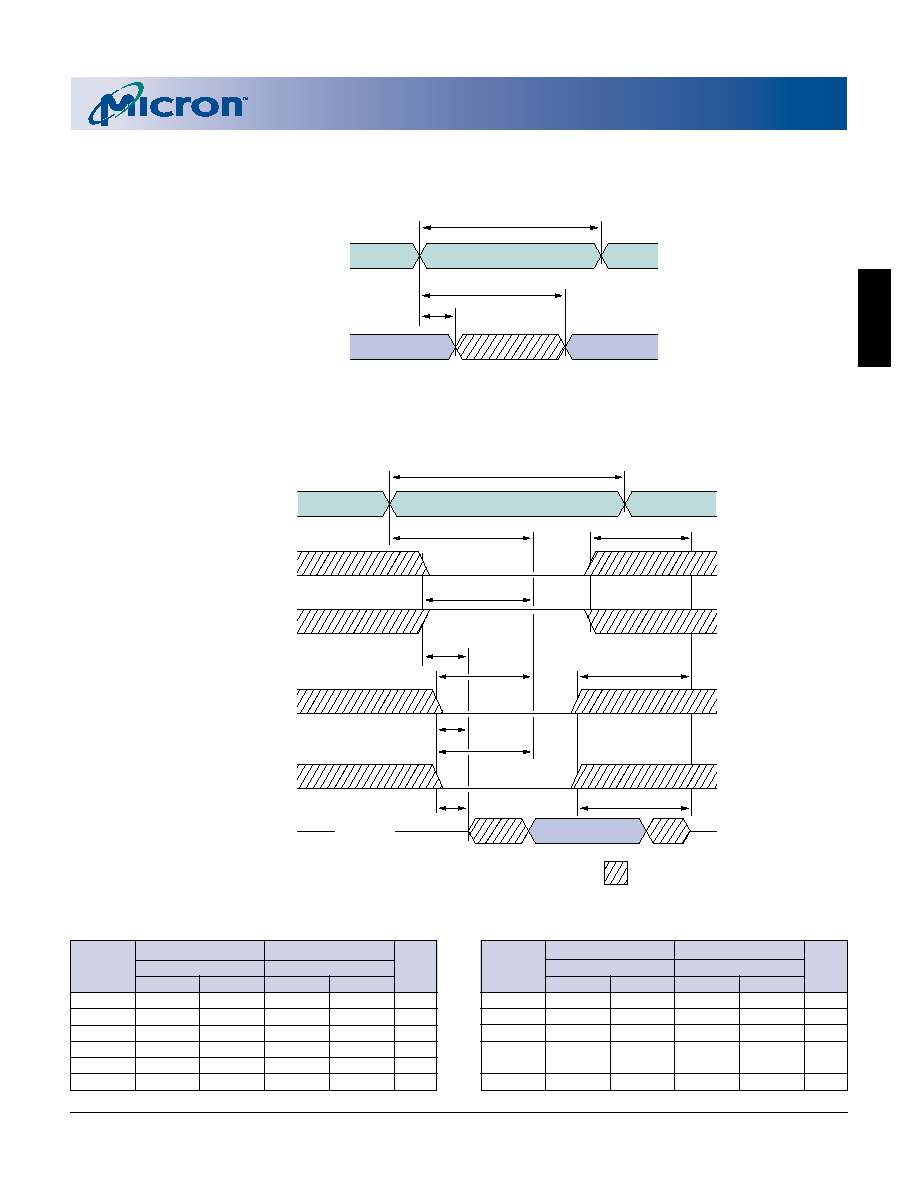
SRAM
44
4 Meg x 16 Asynchronous/Page Flash 512K x 16 SRAM Combo Memory
Micron Technology, Inc., reserves the right to change products or specifications without notice.
MT28C6428P20_3.p65 ≠ Rev. 3, Pub. 7/02
©2002, Micron Technology, Inc.
4 MEG x 16 ASYNCHRONOUS/PAGE FLASH
512K x 16 SRAM COMBO MEMORY
ADVANCE
DON'T CARE
ADDRESS
S_CE1#
S_CE2
S_OE#
S_LB#, S_UB#
DATA-OUT
tRC
tAA
tHZ (1, 2)
tCO
tLBLZ, tUBLZ
tLBHZ, tUBHZ
DATA VALID
High-Z
tOE
tLZ(2)
tOLZ
tOHZ (1)
tLB, tUB
READ CYCLE
1
(S_CE1# = S_OE# = V
IL
; S_CE2, S_WE# = V
IH
)
ADDRESS
DATA-OUT
tRC
tAA
tOH
PREVIOUS
DATA VALID
DATA VALID
READ CYCLE
2
(S_WE# = V
IH
)
t
OLZ
0
0
ns
t
HZ
0
15
0
15
ns
t
OHZ
0
15
0
15
ns
t
LBHZ,
0
15
0
15
ns
t
UBHZ
t
OH
5
5
ns
-80
-85
S_V
CC
= 1.80V≠2.20V
S_V
CC
= 1.70V≠1.90V
SYMBOL
MIN
MAX
MIN
MAX
UNITS
READ TIMING PARAMETERS
-80
-85
S_V
CC
= 1.80V≠2.20V
S_V
CC
= 1.70V≠1.90V
SYMBOL
MIN
MAX
MIN
MAX
UNITS
t
RC
80
85
ns
t
AA
80
85
ns
t
CO
80
85
ns
t
OE
20
20
ns
t
LB,
t
UB
80
85
ns
t
LZ
0
0
ns
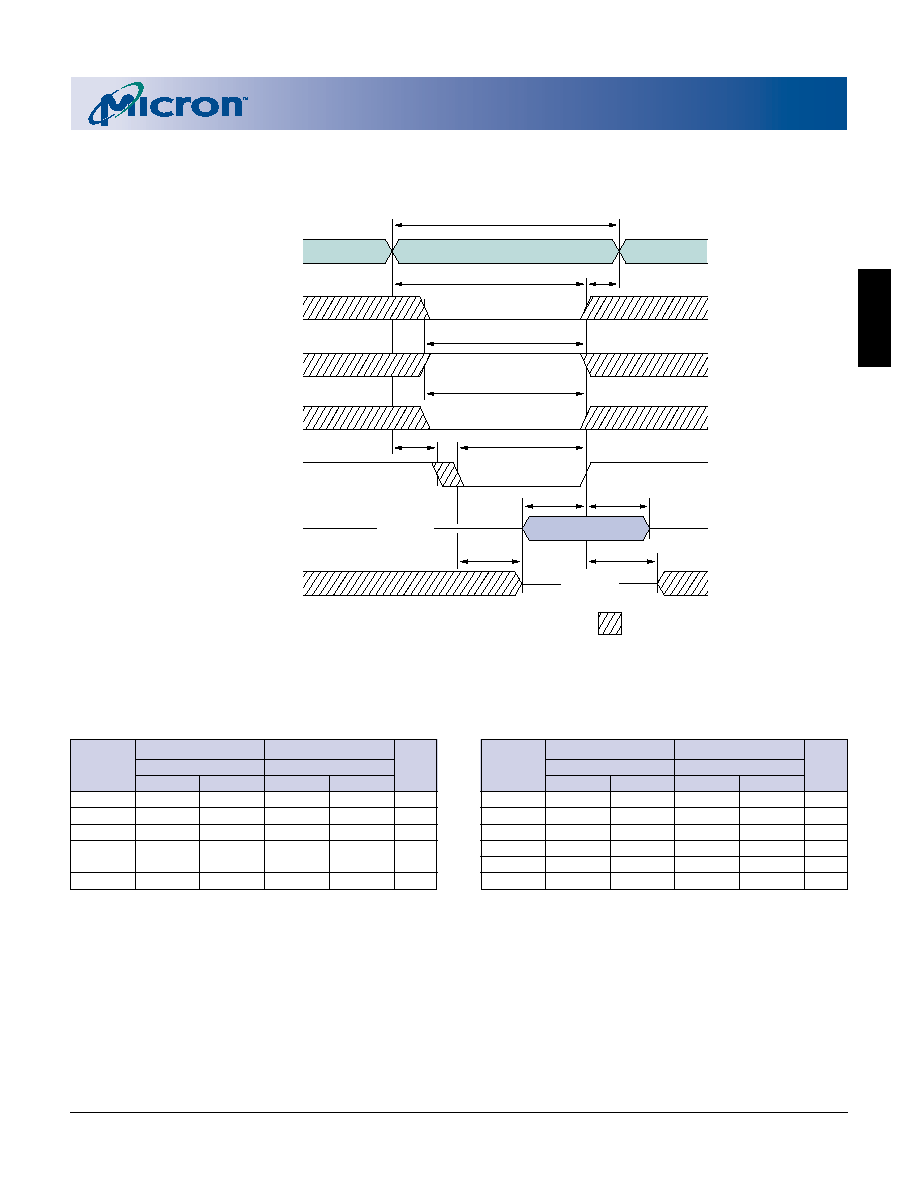
SRAM
45
4 Meg x 16 Asynchronous/Page Flash 512K x 16 SRAM Combo Memory
Micron Technology, Inc., reserves the right to change products or specifications without notice.
MT28C6428P20_3.p65 ≠ Rev. 3, Pub. 7/02
©2002, Micron Technology, Inc.
4 MEG x 16 ASYNCHRONOUS/PAGE FLASH
512K x 16 SRAM COMBO MEMORY
ADVANCE
WRITE CYCLE
(S_WE# CONTROL)
DON'T CARE
ADDRESS
S_CE1#
S_CE2
DATA-OUT
tWC
tAW
tWR
tCW
tWHZ
tOW
High-Z
S_LB#, S_UB#
tLBW, tUBW
S_WE#
DATA-IN
tAS
tWP
tDH
tDW
DATA VALID
High-Z
t
WP
50
50
ns
t
WR
0
0
ns
t
WHZ
0
15
0
15
ns
t
DW
30
30
ns
t
DH
0
0
ns
t
OW
0
0
ns
-80
-85
S_V
CC
= 1.80V≠2.20V
S_V
CC
= 1.70V≠1.90V
SYMBOL
MIN
MAX
MIN
MAX
UNITS
WRITE TIMING PARAMETERS
-80
-85
S_V
CC
= 1.80V≠2.20V
S_V
CC
= 1.70V≠1.90V
SYMBOL
MIN
MAX
MIN
MAX
UNITS
t
WC
80
85
ns
t
CW
80
85
ns
t
AW
80
85
ns
t
LBW,
80
85
ns
t
UBW
t
AS
0
0
ns

SRAM
46
4 Meg x 16 Asynchronous/Page Flash 512K x 16 SRAM Combo Memory
Micron Technology, Inc., reserves the right to change products or specifications without notice.
MT28C6428P20_3.p65 ≠ Rev. 3, Pub. 7/02
©2002, Micron Technology, Inc.
4 MEG x 16 ASYNCHRONOUS/PAGE FLASH
512K x 16 SRAM COMBO MEMORY
ADVANCE
WRITE CYCLE
2
(S_CE1# CONTROL)
DON'T CARE
ADDRESS
S_CE1#
DATA-OUT
tWC
tAW
tWR
tCW
tWHZ
tLZ
High-Z
S_LB#, S_UB#
S_WE#
DATA-IN
tAS
tWP
tLBW, tUBW
tDH
tDW
DATA VALID
t
WP
50
50
ns
t
WR
0
0
ns
t
WHZ
0
15
0
15
ns
t
DW
30
30
ns
t
DH
0
0
ns
t
OW
0
0
ns
-80
-85
S_V
CC
= 1.80V≠2.20V
S_V
CC
= 1.70V≠1.90V
SYMBOL
MIN
MAX
MIN
MAX
UNITS
WRITE TIMING PARAMETERS
-80
-85
S_V
CC
= 1.80V≠2.20V
S_V
CC
= 1.70V≠1.90V
SYMBOL
MIN
MAX
MIN
MAX
UNITS
t
WC
80
85
ns
t
CW
80
85
ns
t
AW
80
85
ns
t
LBW,
80
85
ns
t
UBW
t
AS
0
0
ns
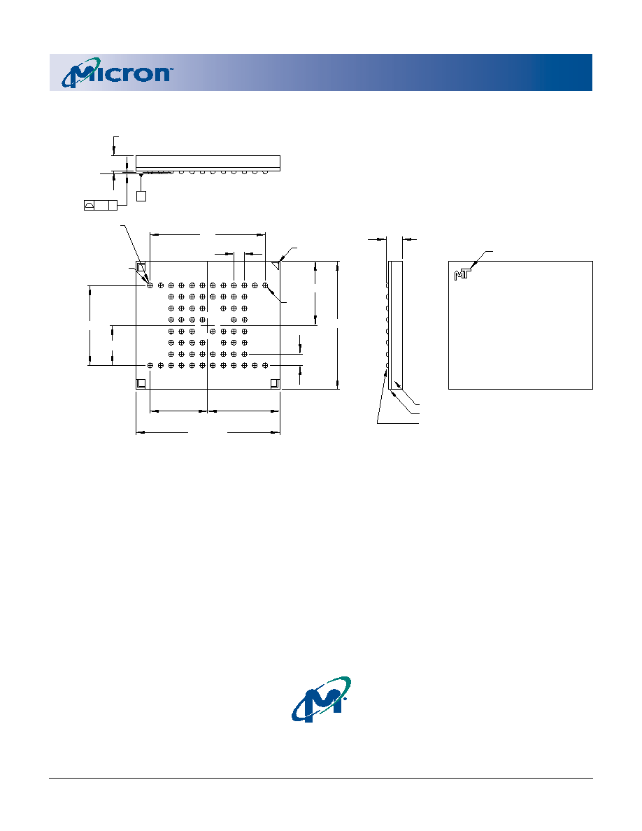
47
4 Meg x 16 Asynchronous/Page Flash 512K x 16 SRAM Combo Memory
Micron Technology, Inc., reserves the right to change products or specifications without notice.
MT28C6428P20_3.p65 ≠ Rev. 3, Pub. 7/02
©2002, Micron Technology, Inc.
4 MEG x 16 ASYNCHRONOUS/PAGE FLASH
512K x 16 SRAM COMBO MEMORY
ADVANCE
67-BALL FBGA
8000 S. Federal Way, P.O. Box 6, Boise, ID 83707-0006, Tel: 208-368-3900
E-mail: prodmktg@micron.com, Internet: http://www.micron.com, Customer Comment Line: 800-932-4992
Micron and the M logo are registered trademarks and the Micron logo is a trademark of Micron Technology, Inc.
0.12 C
SEATING PLANE
C
1.05 ±0.075
67X
0.35
BALL A12
5.60
2.80 ±0.05
4.40 ±0.05
5.75 ±0.05
9.00 ±0.10
4.50 ±0.05
BALL A1 ID
BALL A1 ID
1.40 MAX
BALL A1
0.80 (TYP)
0.80 (TYP)
8.80
11.50 ±0.10
MOLD COMPOUND: EPOXY NOVOLAC
SUBSTRATE: PLASTIC LAMINATE
SOLDER BALL MATERIAL: EUTECTIC 63% Sn, 37% Pb or
62% Sn, 36% Pb, 2%Ag
SOLDER BALL PAD: ÿ .27mm
SOLDER BALL DIAMETER
REFERS TO POST REFLOW
CONDITION. THE PRE-
REFLOW DIAMETER IS ÿ 0.33
C
L
C
L
NOTE: 1. All dimensions in millimeters.
2. Package width and length do not include mold protrusion; allowable mold protrusion is 0.27mm per side.
DATA SHEET DESIGNATION
Advance: This data sheet contains initial descriptions of products still under development.

48
4 Meg x 16 Asynchronous/Page Flash 512K x 16 SRAM Combo Memory
Micron Technology, Inc., reserves the right to change products or specifications without notice.
MT28C6428P20_3.p65 ≠ Rev. 3, Pub. 7/02
©2002, Micron Technology, Inc.
4 MEG x 16 ASYNCHRONOUS/PAGE FLASH
512K x 16 SRAM COMBO MEMORY
ADVANCE
REVISION HISTORY
Rev. 3, ADVANCE .............................................................................................................................................................. 7/02
∑ Corrected bottom boot block device address ranges
∑ Updated command descriptions
∑ Updated SR5 status register bit description
∑ Updated flowcharts
∑ Updated DC Characteristics
∑ Corrected Status Register section
∑ Updated the Read-While-Write/Erase Concurrency section
∑ Changed
t
RHS from 200ns (MIN) to 0ns (MIN)
∑ Changed C
OUT
from 9 (TYP) and 12 (MAX) to 13 (TYP) and 15 (MAX)
Rev. 2, ADVANCE .............................................................................................................................................................. 4/02
∑ Updated the Combined DC Characteristics table
∑ Updated
t
AH and
t
RWH
∑ Updated the chip protection mode register information
∑ Updated the block locking information
Initial published release, ADVANCE, Rev. 1 ............................................................................................................... 1/02