Document Outline
- Features/Options
- General Description
- Pin Assignments
- Functional Block Diagram
- Pin Descriptions
- Truth Table (MT28F200B5)
- Truth Table (MT28F002B5)
- Functional Description
- Overview
- Smart 5 Technology (B5)
- Five Independently Erasable Memory Blocks
- Hardware-Protected Boot Block
- Selectable Bus Size (MT28F200B5 Only)
- Internal State Machine (ISM)
- ISM Status Register
- Command Execution Logic
- Deep Power-Down Mode
- Memory Architecture
- Boot Block
- Figure 1, Memory Address Maps
- Parameter Blocks
- Main Memory Blocks
- Output (READ) Operations
- Memory Array
- Status Register
- Identification Register
- Input Operations
- Cimmands
- Memory Array
- Table 1, Command Set
- Command Set
- ISM Status Register
- Table 2, Status Register
- Command Execution
- READ ARRAY
- Identify Device
- WRITE Sequence
- Table 3, Command Sequence
- ERASE Sequence
- ERASE Suspension
- Error Handling
- Table 4, Status Register Decode
- WRITE/ERASE Cycle Endurance
- Power Usage
- Power-Up
- Figure 2, Power-Up/Reset Timing Diagram
- Self-Timed WRITE Sequence (WORD or BYTE WRITE)
- Complete WRITE Status-Check Sequence
- Self-Timed BLOCK ERASE Sequence
- Complete BLOCK ERASE Status-Check Sequence
- ERASE Suspend/Resume Sequence
- Absolute Maximum Ratings
- Electrical Characteristics and Recommended DC READ Operating Conditions
- DC Operating Characteristics
- Capacitance
- READ and Standby Current Drain
- READ Timing Parameters, Electrical Characteristics and Recommended AC Operating Conditions
- Test Condition 1
- Test Condition 2
- AC Test Condition 1
- AC Test Condition 2
- WORD-WIDE READ Cycle
- BYTE-WIDE READ Cycle
- Recommended DC WRITE/ERASE Conditions
- WRITE/ERASE Current Drain
- Speed-Dependent WRITE/ERASE AC Timing Characteristics and Recommended AC Operating Conditions
- Test Condition 1
- Test Condition 2
- WE#-Controlled WRITEs
- CE#-Controlled WRITEs
- WORD/BYTE WRITE and ERASE Duration Characteristics
- WRITE/ERASE Cycle, WE#-Controlled WRITE/ERASE
- WRITE/ERASE Cycle, CE#-Controlled WRITE/ERASE
- Package Drawings
- 40-Pin Plastic TSOP I (10mm x 20mm)
- 44-Pin Plastic SOP I (600 mil)
- 48-Pin Plastic TSOP I (12mm x 20mm)
1
2Mb Smart 5 Boot Block Flash Memory Micron Technology, Inc., reserves the right to change products or specifications without notice.
F50.p65 ≠ Rev. 1/00 ©2000, Micron Technology, Inc.
2Mb
SMART 5 BOOT BLOCK FLASH MEMORY
FLASH MEMORY MT28F002B5
MT28F200B5
5V Only, Dual Supply (Smart 5)
FEATURES
∑ Five erase blocks:
16KB/8K-word boot block (protected)
Two 8KB/4K-word parameter blocks
Two main memory blocks
∑ Smart 5 technology (B5):
5V
±
10% V
CC
5V
±
10% V
PP
application/production
programming
12V
±
5% V
PP
compatibility production
programming
∑ Address access times: 60ns, 80ns
∑ 100,000 ERASE cycles
∑ Industry-standard pinouts
∑ Inputs and outputs are fully TTL-compatible
∑ Automated write and erase algorithm
∑ Two-cycle WRITE/ERASE sequence
∑ Byte- or word-wide READ and WRITE
(MT28F200B5, 128K x 16/256K x 8)
∑ Byte-wide READ and WRITE only
(MT28F002B5, 256K x 8)
∑ TSOP and SOP packaging options
OPTIONS MARKING
∑ Timing
60ns access -6
80ns access -8
80ns access -8 ET
∑ Configurations
256K x 8 MT28F002B5
128K x 16/256K x 8 MT28F200B5
∑ Boot Block Starting Word Address
Top (1FFFFH) T
Bottom (00000H) B
∑ Operating Temperature Range
Commercial (0
∞
C to +70
∞
C) None
Extended (-40
∞
C to +85
∞
C) ET
∑ Packages
Plastic 44-pin SOP (600 mil) SG
Plastic 48-pin TSOP Type 1 WG
(12mm x 20mm)
Plastic 40-pin TSOP VG
(10mm x 20mm)
Part Number Example:
MT28F200B5SG-8 T
GENERAL DESCRIPTION
The MT28F002B5 (x8) and MT28F200B5 (x16/x8)
are nonvolatile, electrically block-erasable (flash), pro-
grammable, read-only memories containing 2,097,152
bits organized as 262,144 bytes (8 bits) or 131,072
words (16 bits). Writing or erasing the device is done
with a 5V V
PP
voltage, while all operations are per-
formed with a 5V V
CC
. Due to process technology
advances, 5V V
PP
is optimal for application and produc-
tion programming. For backward compatibility with
SmartVoltage technology, 12V V
PP
is supported for a
maximum of 100 cycles and may be connected for up
to 100 cumulative hours. These devices are fabricated
with Micron's advanced CMOS floating-gate process.
The MT28F002B5 and MT28F200B5 are organized
into five separately erasable blocks. To ensure that
critical firmware is protected from accidental erasure or
overwrite, the devices feature a hardware-protected
boot block. Writing or erasing the boot block requires
either applying a super-voltage to the RP# pin or driv-
ing WP# HIGH in addition to executing the normal
write or erase sequences. This block may be used to store
code implemented in low-level system recovery. The
remaining blocks vary in density and are written and
erased with no additional security measures.
Please refer to Micron's Web site
(www.micron.com/
flash/htmls/datasheets.html)
for the latest data sheet.
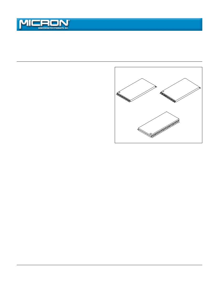
40-Pin TSOP Type I 48-Pin TSOP Type I
44-Pin SOP
2
2Mb Smart 5 Boot Block Flash Memory
Micron Technology, Inc., reserves the right to change products or specifications without notice.
F50.p65 ≠ Rev. 1/00
©2000, Micron Technology, Inc.
2Mb
SMART 5 BOOT BLOCK FLASH MEMORY
A15
A14
A13
A12
A11
A10
A9
A8
NC
NC
WE#
RP#
V
PP
WP#
NC
NC
NC
A7
A6
A5
A4
A3
A2
A1
A16
BYTE#
V
SS
DQ15/(A - 1)
DQ7
DQ14
DQ6
DQ13
DQ5
DQ12
DQ4
V
CC
DQ11
DQ3
DQ10
DQ2
DQ9
DQ1
DQ8
DQ0
OE#
V
SS
CE#
A0
1
2
3
4
5
6
7
8
9
10
11
12
13
14
15
16
17
18
19
20
21
22
23
24
48
47
46
45
44
43
42
41
40
39
38
37
36
35
34
33
32
31
30
29
28
27
26
25
V
PP
WP#
NC
A7
A6
A5
A4
A3
A2
A1
A0
CE#
V
SS
OE#
DQ0
DQ8
DQ1
DQ9
DQ2
DQ10
DQ3
DQ11
RP#
WE#
A8
A9
A10
A11
A12
A13
A14
A15
A16
BYTE#
V
SS
DQ15/(A - 1)
DQ7
DQ14
DQ6
DQ13
DQ5
DQ12
DQ4
V
CC
1
2
3
4
5
6
7
8
9
10
11
12
13
14
15
16
17
18
19
20
21
22
44
43
42
41
40
39
38
37
36
35
34
33
32
31
30
29
28
27
26
25
24
23
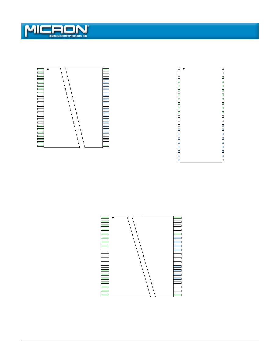
PIN ASSIGNMENT (Top View)
40-Pin TSOP Type I
48-Pin TSOP Type I
44-Pin SOP
ORDER NUMBER AND PART MARKING
MT28F200B5SG-6 B
MT28F200B5SG-6 T
MT28F200B5SG-8 B
MT28F200B5SG-8 T
MT28F200B5SG-8 BET
MT28F200B5SG-8 TET
ORDER NUMBER AND PART MARKING
MT28F200B5WG-6 B
MT28F200B5WG-6 T
MT28F200B5WG-8 B
MT28F200B5WG-8 T
MT28F200B5WG-8 BET
MT28F200B5WG-8 TET
ORDER NUMBER AND PART MARKING
MT28F002B5VG-6 B
MT28F002B5VG-6 T
MT28F002B5VG-8 B
MT28F002B5VG-8 T
MT28F002B5VG-8 BET
MT28F002B5VG-8 TET
A16
A15
A14
A13
A12
A11
A9
A8
WE#
RP#
V
PP
WP#
NC
A7
A6
A5
A4
A3
A2
A1
A17
V
SS
NC
NC
A10
DQ7
DQ6
DQ5
DQ4
V
CC
V
CC
NC
DQ3
DQ2
DQ1
DQ0
OE#
V
SS
CE#
A0
1
2
3
4
5
6
7
8
9
10
11
12
13
14
15
16
17
18
19
20
40
39
38
37
36
35
34
33
32
31
30
29
28
27
26
25
24
23
22
21
3
2Mb Smart 5 Boot Block Flash Memory
Micron Technology, Inc., reserves the right to change products or specifications without notice.
F50.p65 ≠ Rev. 1/00
©2000, Micron Technology, Inc.
2Mb
SMART 5 BOOT BLOCK FLASH MEMORY
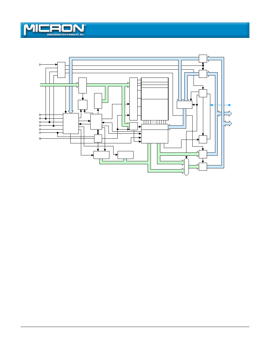
FUNCTIONAL BLOCK DIAGRAM
16KB Boot Block
8KB Parameter Block
8KB Parameter Block
96KB Main Block
Y - Select Gates
Sense Amplifiers
Write/Erase-Bit
Compare and Verify
Addr.
Buffer/
Latch
Power
(Current)
Control
Addr.
Counter
Command
Execution
Logic
I/O
Control
Logic
V
PP
Switch/
Pump
Status
Register
Identification
Register
Y -
Decoder
128KB Main Block
X - Decoder/Block Erase Control
Output
Buffer
Input
Buffer
State
Machine
BYTE#
1
A0-A16/(A17)
CE#
OE#
WE#
RP#
V
PP
DQ15/(A - 1)
1
MUX
DQ15
8
8
7
DQ8-DQ14
1
DQ0-DQ7
16
8
18 (19)
7
(A - 1)
9
(10)
9
8
Output
Buffer
Output
Buffer
Input
Buffer
Input
Buffer
Input Data
Latch/Mux
7
A9
V
CC
WP#
NOTE
1. Does not apply to MT28F002B5.
4
2Mb Smart 5 Boot Block Flash Memory
Micron Technology, Inc., reserves the right to change products or specifications without notice.
F50.p65 ≠ Rev. 1/00
©2000, Micron Technology, Inc.
2Mb
SMART 5 BOOT BLOCK FLASH MEMORY
PIN DESCRIPTIONS
44-PIN SOP 40-PIN TSOP 48-PIN TSOP
NUMBERS
NUMBERS
NUMBERS
SYMBOL
TYPE
DESCRIPTION
43
9
11
WE#
Input
Write Enable: Determines if a given cycle is a WRITE cycle. If
WE# is LOW, the cycle is either a WRITE to the command
execution logic (CEL) or to the memory array.
2
12
14
WP#
Input
Write Protect: Unlocks the boot block when HIGH if V
PP
=
V
PPH
1
(5V) or V
PPH
2
(12V)
1
and RP# = V
IH
during a WRITE or
ERASE. Does not affect WRITE or ERASE operation on other
blocks.
12
22
26
CE#
Input
Chip Enable: Activates the device when LOW. When CE# is
HIGH, the device is disabled and goes into standby power
mode.
44
10
12
RP#
Input
Reset/Power-Down: When LOW, RP# clears the status register,
sets the internal state machine (ISM) to the array read mode
and places the device in deep power-down mode. All inputs,
including CE#, are "Don't Care," and all outputs are High-Z.
RP# unlocks the boot block and overrides the condition of
WP# when at V
HH
(12V), and must be held at V
IH
during all
other modes of operation.
14
24
28
OE#
Input
Output Enable: Enables data output buffers when LOW.
When OE# is HIGH, the output buffers are disabled.
33
≠
47
BYTE#
Input
Byte Enable: If BYTE# = HIGH, the upper byte is active through
DQ8-DQ15. If BYTE# = LOW, DQ8-DQ14 are High-Z, and all
data is accessed through DQ0-DQ7. DQ15/(A - 1) becomes the
least significant address input.
11, 10, 9, 8,
21, 20, 19,
25, 24, 23,
A0-A16/
Input
Address Inputs: Select a unique, 16-bit word or 8-bit byte. The
7, 6, 5, 4,
18, 17, 16,
22, 21, 20,
(A17)
DQ15/(A - 1) input becomes the lowest order address when
42, 41, 40,
15, 14, 8, 7,
19, 18, 8, 7,
BYTE# = LOW (MT28F200B5) to allow for a selection of an
39, 38, 37,
36, 6, 5, 4, 3,
6, 5, 4, 3, 2,
8-bit byte from the 262,144 available.
36, 35, 34
2, 1, 40
1, 48
31
≠
45
DQ15
Input/
Data I/O: MSB of data when BYTE# = HIGH. Address Input: LSB
(A - 1)
Output of address input when BYTE# = LOW during READ or WRITE
operation.
15, 17, 19,
25-28, 32-35
29, 31, 33,
DQ0-DQ7
Input/
Data I/Os: Data output pins during any READ operation or
21, 24, 26,
35, 38, 40,
Output data input pins during a WRITE. These pins are used to input
28, 30
42, 44
commands to the CEL.
16, 18, 20,
≠
30, 32, 34,
DQ8-DQ14
Input/
Data I/Os: Data output pins during any READ operation or
22, 25, 27,
36, 39, 41,
Output data input pins during a WRITE when BYTE# = HIGH. These
29
43
pins are High-Z when BYTE# is LOW.
1
11
13
V
PP
Supply Write/Erase Supply Voltage: From a WRITE or ERASE CONFIRM
until completion of the WRITE or ERASE, V
PP
must be at V
PPH
1
(5V) or V
PPH
2
(12V)
1
. V
PP
= "Don't Care" during all other
operations.
23
30, 31
37
V
CC
Supply Power Supply: +5V
±
10%.
13, 32
23, 39
27, 46
V
SS
Supply Ground.
3
13, 29, 37, 38 9, 10, 15-17
NC
≠
No Connect: These pins may be driven or left unconnected.
NOTE: 1. For SmartVoltage-compatible production programming, 12V V
PP
is supported for a maximum of 100 cycles and may
be connected for up to 100 cumulative hours.
5
2Mb Smart 5 Boot Block Flash Memory
Micron Technology, Inc., reserves the right to change products or specifications without notice.
F50.p65 ≠ Rev. 1/00
©2000, Micron Technology, Inc.
2Mb
SMART 5 BOOT BLOCK FLASH MEMORY
NOTE: 1. L = V
IL
(LOW), H = V
IH
(HIGH), X = V
IL
or V
IH
("Don't Care").
2. V
PPH
= V
PPH
1
= 5V.
3. Operation must be preceded by ERASE SETUP command.
4. Operation must be preceded by WRITE SETUP command.
5. The READ ARRAY command must be issued before reading the array after writing or erasing.
6. When WP# = V
IH
, RP# may be at V
IH
or V
HH
.
7. V
HH
= 12V.
8. V
ID
= 12V; may also be read by issuing the IDENTIFY DEVICE command.
9. A1-A8, A10-A16 = V
IL
.
10. Value reflects DQ8-DQ15.
TRUTH TABLE (MT28F200B5)
1
FUNCTION
RP#
CE#
OE#
WE# WP# BYTE# A0
A9
V
PP
DQ0-DQ7 DQ8-DQ14 DQ15/A - 1
Standby
H
H
X
X
X
X
X
X
X
High-Z
High-Z
High-Z
RESET
L
X
X
X
X
X
X
X
X
High-Z
High-Z
High-Z
READ
READ (word mode)
H
L
L
H
X
H
X
X
X
Data-Out
Data-Out
Data-Out
READ (byte mode)
H
L
L
H
X
L
X
X
X
Data-Out
High-Z
A - 1
Output Disable
H
L
H
H
X
X
X
X
X
High-Z
High-Z
High-Z
WRITE/ERASE (EXCEPT BOOT BLOCK)
2
ERASE SETUP
H
L
H
L
X
X
X
X
X
20H
X
X
ERASE CONFIRM
3
H
L
H
L
X
X
X
X
V
PPH
D0H
X
X
WRITE SETUP
H
L
H
L
X
X
X
X
X
10H/40H
X
X
WRITE (word mode)
4
H
L
H
L
X
H
X
X
V
PPH
Data-In
Data-In
Data-In
WRITE (byte mode)
4
H
L
H
L
X
L
X
X
V
PPH
Data-In
X
A - 1
READ ARRAY
5
H
L
H
L
X
X
X
X
X
FFH
X
X
WRITE/ERASE (BOOT BLOCK)
2, 7
ERASE SETUP
H
L
H
L
X
X
X
X
X
20H
X
X
ERASE CONFIRM
3
V
HH
L
H
L
X
X
X
X
V
PPH
D0H
X
X
ERASE CONFIRM
3, 6
H
L
H
L
H
X
X
X
V
PPH
D0H
X
X
WRITE SETUP
H
L
H
L
X
X
X
X
X
10H/40H
X
X
WRITE (word mode)
4
V
HH
L
H
L
X
H
X
X
V
PPH
Data-In
Data-In
Data-In
WRITE (word mode)
4, 6
H
L
H
L
H
H
X
X
V
PPH
Data-In
Data-In
Data-In
WRITE (byte mode)
4
V
HH
L
H
L
X
L
X
X
V
PPH
Data-In
X
A - 1
WRITE (byte mode)
4, 6
H
L
H
L
H
L
X
X
V
PPH
Data-In
X
A - 1
READ ARRAY
5
H
L
H
L
X
X
X
X
X
FFH
X
X
DEVICE IDENTIFICATION
8, 9
Manufacturer Compatibility
H
L
L
H
X
H
L
V
ID
X
89H
00H
≠
(word mode)
10
Manufacturer Compatibility
H
L
L
H
X
L
L
V
ID
X
89H
High-Z
X
(byte mode)
Device (word mode, top boot)
10
H
L
L
H
X
H
H
V
ID
X
74H
22H
≠
Device (byte mode, top boot)
H
L
L
H
X
L
H
V
ID
X
74H
High-Z
X
Device (word mode, bottom boot)
10
H
L
L
H
X
H
H
V
ID
X
75H
22H
≠
Device (byte mode, bottom boot)
H
L
L
H
X
L
H
V
ID
X
75H
High-Z
X
6
2Mb Smart 5 Boot Block Flash Memory
Micron Technology, Inc., reserves the right to change products or specifications without notice.
F50.p65 ≠ Rev. 1/00
©2000, Micron Technology, Inc.
2Mb
SMART 5 BOOT BLOCK FLASH MEMORY
NOTE: 1. L = V
IL
, H = V
IH
, X = V
IL
or V
IH
.
2. V
PPH
= V
PPH
1
= 5V.
3. Operation must be preceded by ERASE SETUP command.
4. Operation must be preceded by WRITE SETUP command.
5. The READ ARRAY command must be issued before reading the array after writing or erasing.
6. When WP# = V
IH
, RP# may be at V
IH
or V
HH
.
7. V
HH
= 12V.
8. V
ID
= 12V; may also be read by issuing the IDENTIFY DEVICE command.
9. A1-A8, A10-A17 = V
IL
.
TRUTH TABLE (MT28F002B5)
1
FUNCTION
RP#
CE#
OE#
WE#
WP#
A0
A9
V
PP
DQ0-DQ7
Standby
H
H
X
X
X
X
X
X
High-Z
RESET
L
X
X
X
X
X
X
X
High-Z
READ
READ
H
L
L
H
X
X
X
X
Data-Out
Output Disable
H
L
H
H
X
X
X
X
High-Z
WRITE/ERASE (EXCEPT BOOT BLOCK)
2
ERASE SETUP
H
L
H
L
X
X
X
X
20H
ERASE CONFIRM
3
H
L
H
L
X
X
X
V
PPH
D0H
WRITE SETUP
H
L
H
L
X
X
X
X
10H/40H
WRITE
4
H
L
H
L
X
X
X
V
PPH
Data-In
READ ARRAY
5
H
L
H
L
X
X
X
X
FFH
WRITE/ERASE (BOOT BLOCK)
2, 7
ERASE SETUP
H
L
H
L
X
X
X
X
20H
ERASE CONFIRM
3
V
HH
L
H
L
X
X
X
V
PPH
D0H
ERASE CONFIRM
3, 6
H
L
H
L
H
X
X
V
PPH
D0H
WRITE SETUP
H
L
H
L
X
X
X
X
10H/40H
WRITE
4
V
HH
L
H
L
X
X
X
V
PPH
Data-In
WRITE
4, 6
H
L
H
L
H
X
X
V
PPH
Data-In
READ ARRAY
5
H
L
H
L
X
X
X
X
FFH
DEVICE IDENTIFICATION
8, 9
Manufacturer Compatibility
H
L
L
H
X
L
V
ID
X
89H
Device (top boot)
H
L
L
H
X
H
V
ID
X
7CH
Device (bottom boot)
H
L
L
H
X
H
V
ID
X
7DH

7
2Mb Smart 5 Boot Block Flash Memory
Micron Technology, Inc., reserves the right to change products or specifications without notice.
F50.p65 ≠ Rev. 1/00
©2000, Micron Technology, Inc.
2Mb
SMART 5 BOOT BLOCK FLASH MEMORY
FUNCTIONAL DESCRIPTION
The MT28F002B5 and MT28F200B5 flash memory
incorporate a number of features ideally suited for
system firmware. The memory array is segmented into
individual erase blocks. Each block may be erased
without affecting data stored in other blocks. These
memory blocks are read, written and erased with com-
mands to the command execution logic (CEL). The CEL
controls the operation of the internal state machine
(ISM), which completely controls all WRITE, BLOCK
ERASE and VERIFY operations. The ISM protects each
memory location from over-erasure and optimizes each
memory location for maximum data retention. In addi-
tion, the ISM greatly simplifies the control necessary
for writing the device in-system or in an external
programmer.
The Functional Description provides detailed infor-
mation on the operation of the MT28F002B5 and
MT28F200B5 and is organized into these sections:
∑
Overview
∑
Memory Architecture
∑
Output (READ) Operations
∑
Input Operations
∑
Command Set
∑
ISM Status Register
∑
Command Execution
∑
Error Handling
∑
WRITE/ERASE Cycle Endurance
∑
Power Usage
∑
Power-Up
OVERVIEW
SMART 5 TECHNOLOGY (B5)
Smart 5 technology allows maximum flexibility for
in-system READ, WRITE and ERASE operations. For 5V-
only systems, WRITE and ERASE operations may be
executed with a V
PP
voltage of 5V. Due to process
technology advances, 5V V
PP
is optimal for application
and production programming. For backward compat-
ibility with SmartVoltage technology, 12V V
PP
is sup-
ported for a maximum of 100 cycles and may be
connected for up to 100 cumulative hours. However,
no performance increase will be realized. For any opera-
tion, V
CC
may be at 5V.
FIVE INDEPENDENTLY ERASABLE MEMORY
BLOCKS
The MT28F002B5 and MT28F200B5 are organized
into five independently erasable memory blocks that
allow portions of the memory to be erased without
affecting the rest of the memory data. A special boot
block is hardware-protected against inadvertent era-
sure or writing by requiring either a super-voltage on
the RP# pin or driving the WP# pin HIGH. One of these
two conditions must exist along with the V
PP
voltage
(5V or 12V) on the V
PP
pin before a WRITE or ERASE will
be performed on the boot block. The remaining blocks
require that only the V
PP
voltage be present on the V
PP
pin before writing or erasing.
HARDWARE-PROTECTED BOOT BLOCK
This block of the memory array can be erased or
written only when the RP# pin is taken to V
HH
or when
the WP# pin is brought HIGH. This provides additional
security for the core firmware during in-system firm-
ware updates should an unintentional power fluctua-
tion or system reset occur. The MT28F002B5 and
MT28F200B5 are available with the boot block starting
at the bottom of the address space ("B" suffix) or the top
of the address space ("T" suffix).
SELECTABLE BUS SIZE (MT28F200B5 ONLY)
The MT28F200B5 allows selection of an 8-bit (256K
x 8) or 16-bit (128K x 16) data bus for reading and
writing the memory. The BYTE# pin is used to select the
bus width. In the x16 configuration, control data is read
or written only on the lower eight bits (DQ0-DQ7).
Data written to the memory array utilizes all active
data pins for the selected configuration. When the x8
configuration is selected, data is written in byte form;
when the x16 configuration is selected, data is written
in word form.
INTERNAL STATE MACHINE (ISM)
BLOCK ERASE and BYTE/WORD WRITE timing are
simplified with an ISM that controls all erase and write
algorithms in the memory array. The ISM ensures
protection against overerasure and optimizes write
margin to each cell.
During WRITE operations, the ISM automatically
increments and monitors WRITE attempts, verifies write
margin on each memory cell and updates the ISM status
register. When BLOCK ERASE is performed, the ISM
automatically overwrites the entire addressed block
(eliminates overerasure), increments and monitors
ERASE attempts, and sets bits in the ISM status register.
ISM STATUS REGISTER
The ISM status register allows an external processor
to monitor the status of the ISM during WRITE and
ERASE operations. Two bits of the 8-bit status register
are set and cleared entirely by the ISM. These bits
indicate whether the ISM is busy with a WRITE or
ERASE task and when an ERASE has been suspended.
Additional error information is set in three other bits:
V
PP
status, write status and erase status.
8
2Mb Smart 5 Boot Block Flash Memory
Micron Technology, Inc., reserves the right to change products or specifications without notice.
F50.p65 ≠ Rev. 1/00
©2000, Micron Technology, Inc.
2Mb
SMART 5 BOOT BLOCK FLASH MEMORY
Figure 1
Memory Address Maps
Top Boot
MT28F002B5/200B5xx-xxT
Bottom Boot
MT28F002B5/200B5xx-xxB
1FFFFH
1E000H
1DFFFH
1D000H
1CFFFH
1C000H
1BFFFH
10000H
0FFFFH
00000H
16KB Boot Block
8KB Parameter Block
8KB Parameter Block
96KB Main Block
128KB Main Block
WORD ADDRESS
3FFFFH
3C000H
3BFFFH
3A000H
39FFFH
38000H
37FFFH
20000H
1FFFFH
00000H
BYTE ADDRESS
1FFFFH
10000H
0FFFFH
04000H
03FFFH
03000H
02FFFH
02000H
01FFFH
00000H
128KB Main Block
96KB Main Block
8KB Parameter Block
8KB Parameter Block
16KB Boot Block
WORD ADDRESS
3FFFFH
20000H
1FFFFH
08000H
07FFFH
06000H
05FFFH
04000H
03FFFH
00000H
BYTE ADDRESS
COMMAND EXECUTION LOGIC (CEL)
The CEL receives and interprets commands to the
device. These commands control the operation of the
ISM and the read path (i.e., memory array, ID register or
status register). Commands may be issued to the CEL
while the ISM is active. However, there are restrictions
on what commands are allowed in this condition. See
the Command Execution section for more detail.
DEEP POWER-DOWN MODE
To allow for maximum power conservation, the
MT28F002B5 and MT28F200B5 feature a very low cur-
rent, deep power-down mode. To enter this mode, the
RP# pin is taken to V
SS
±
0.2V. In this mode, the current
draw is a maximum of 20
µ
A at 5V V
CC
. Entering deep
power-down also clears the status register and sets the
ISM to the read array mode.
MEMORY ARCHITECTURE
The MT28F002B5 and MT28F200B5 memory array
architecture is designed to allow sections to be erased
without disturbing the rest of the array. The array is
divided into five addressable blocks that vary in size
and are independently erasable. When blocks rather
than the entire array are erased, total device endurance
is enhanced, as is system flexibility. Only the ERASE
function is block-oriented. All READ and WRITE opera-
tions are done on a random-access basis.
The boot block is protected from unintentional
ERASE or WRITE with a hardware protection circuit
which requires that a super-voltage be applied to RP# or
that the WP# pin be driven HIGH before erasure is
commenced. The boot block is intended for the core
firmware required for basic system functionality. The
remaining four blocks do not require that either of
these two conditions be met before WRITE or ERASE
operations.
BOOT BLOCK
The hardware-protected boot block provides extra
security for the most sensitive portions of the firmware.
This 16KB block may only be erased or written when the
RP# pin is at the specified boot block unlock voltage
(V
HH
) of 12V or when the WP# pin is V
IH
. During a
WRITE or ERASE of the boot block, the RP# pin must be

9
2Mb Smart 5 Boot Block Flash Memory
Micron Technology, Inc., reserves the right to change products or specifications without notice.
F50.p65 ≠ Rev. 1/00
©2000, Micron Technology, Inc.
2Mb
SMART 5 BOOT BLOCK FLASH MEMORY
After power-up or RESET, the device will automati-
cally be in the array read mode. All commands and their
operations are covered in the Command Set and Com-
mand Execution sections.
STATUS REGISTER
Performing a READ of the status register requires the
same input sequencing as a READ of the array except
that the address inputs are "Don't Care." The status
register contents are always output on DQ0-DQ7, re-
gardless of the condition of BYTE# on the MT28F200B5.
DQ8-DQ15 are LOW when BYTE# is HIGH, and DQ8-
DQ14 are High-Z when BYTE# is LOW. Data from the
status register is latched on the falling edge of OE# or
CE#, whichever occurs last. If the contents of the status
register change during a READ of the status register,
either OE# or CE# may be toggled while the other is
held LOW to update the output.
Following a WRITE or ERASE, the device automati-
cally enters the status register read mode. In addition,
a READ during a WRITE or ERASE will produce the
status register contents on DQ0-DQ7. When the device
is in the erase suspend mode, a READ operation will
produce the status register contents until another com-
mand is issued. In certain other modes, READ STATUS
REGISTER may be given to return to the status register
read mode. All commands and their operations are
covered in the Command Set and Command Execution
sections.
IDENTIFICATION REGISTER
A READ of the two 8-bit device identification regis-
ters requires the same input sequencing as a READ of
the array. WE# must be HIGH, and OE# and CE# must
be LOW. However, ID register data is output only on
DQ0-DQ7, regardless of the condition of BYTE# on the
MT28F200B5. A0 is used to decode between the two
bytes of the device ID register; all other address inputs
are "Don't Care." When A0 is LOW, the manufacturer
compatibility ID is output, and when A0 is HIGH, the
device ID is output. DQ8-DQ15 are High-Z when BYTE#
is LOW. When BYTE# is HIGH, DQ8-DQ15 are 00H
when the manufacturer compatibility ID is read and
22H when the device ID is read.
To get to the identification register read mode,
READ IDENTIFICATION may be issued while the device
is in certain other modes. In addition, the identifica-
tion register read mode can be reached by applying a
super-voltage (V
ID
) to the A9 pin. Using this method,
the ID register can be read while the device is in any
mode. Once A9 is returned to V
IL
or V
IH
, the device will
return to the previous mode.
held at V
HH
or the WP# pin held HIGH until the ERASE
or WRITE is completed. The V
PP
pin must be at V
PPH
(5V
or 12V) when the boot block is written to or erased.
The MT28F002B5 and MT28F200B5 are available in
two configurations and top or bottom boot block. The
top boot block version supports processors of the x86
variety. The bottom boot block version is intended for
680X0 and RISC applications. Figure 1 illustrates the
memory address maps associated with these two
versions.
PARAMETER BLOCKS
The two 8KB parameter blocks store less sensitive
and more frequently changing system parameters and
also may store configuration or diagnostic coding.
These blocks are enabled for erasure when the V
PP
pin
is at V
PPH
. No super-voltage unlock or WP# control is
required.
MAIN MEMORY BLOCKS
The two remaining blocks are general-purpose
memory blocks and do not require a super-voltage on
RP# or WP# control to be erased or written. These
blocks are intended for code storage, ROM-resident
applications or operating systems that require in-
system update capability.
OUTPUT (READ) OPERATIONS
The MT28F002B5 and MT28F200B5 feature three
different types of READs. Depending on the current
mode of the device, a READ operation will produce data
from the memory array, status register or device iden-
tification register. In each of these three cases, the WE#,
CE# and OE# inputs are controlled in a similar manner.
Moving between modes to perform a specific READ is
covered in the Command Execution section.
MEMORY ARRAY
To read the memory array, WE# must be HIGH, and
OE# and CE# must be LOW. Valid data will be output
on the DQ pins once these conditions have been met
and a valid address is given. Valid data will remain on
the DQ pins until the address changes, or until OE# or
CE# goes HIGH, whichever occurs first. The DQ pins
will continue to output new data after each address
transition as long as OE# and CE# remain LOW.
The MT28F200B5 features selectable bus widths.
When the memory array is accessed as a 128K x 16,
BYTE# is HIGH, and data will be output on DQ0-DQ15.
To access the memory array as a 256K x 8, BYTE# must
be LOW, DQ8-DQ14 are High-Z, and all data is output
on DQ0-DQ7. The DQ15/(A - 1) pin becomes the lowest
order address input so that 262,144 locations can be
read.
10
2Mb Smart 5 Boot Block Flash Memory
Micron Technology, Inc., reserves the right to change products or specifications without notice.
F50.p65 ≠ Rev. 1/00
©2000, Micron Technology, Inc.
2Mb
SMART 5 BOOT BLOCK FLASH MEMORY
INPUT OPERATIONS
The DQ pins are used either to input data to the
array or to input a command to the CEL. A command
input issues an 8-bit command to the CEL to control the
mode of operation of the device. A WRITE is used to
input data to the memory array. The following section
describes both types of inputs. More information de-
scribing how to use the two types of inputs to write or
erase the device is provided in the Command Execution
section.
COMMANDS
To perform a command input, OE# must be HIGH,
and CE# and WE# must be LOW. Addresses are "Don't
Care" but must be held stable, except during an ERASE
CONFIRM (described in a later section). The 8-bit com-
mand is input on DQ0-DQ7, while DQ8-DQ15 are
"Don't Care" on the MT28F200B5. The command is
latched on the rising edge of CE# (CE#-controlled) or
WE# (WE#-controlled), whichever occurs first. The
condition of BYTE# on the MT28F200B5 has no effect
on a command input.
MEMORY ARRAY
A WRITE to the memory array sets the desired bits to
logic 0s but cannot change a given bit to a logic 1 from
a logic 0. Setting any bits to a logic 1 requires that the
entire block be erased. To perform a WRITE, OE# must
be HIGH, CE# and WE# must be LOW, and V
PP
must be
set to V
PPH
1
or V
PPH
2
. Writing to the boot block also
requires that the RP# pin be at V
HH
or WP# be HIGH. A0-
A16/(A17) provide the address to be written, while the
data to be written to the array is input on the DQ pins.
The data and addresses are latched on the rising edge of
CE# (CE#-controlled) or WE# (WE#-controlled), which-
ever occurs first. A WRITE must be preceded by a WRITE
SETUP command. Details on how to input data to the
array will be covered in the Write Sequence section.
Selectable bus sizing applies to WRITEs as it does to
READs on the MT28F200B5. When BYTE# is LOW (byte
mode), data is input on DQ0-DQ7, DQ8-DQ14 are
High-Z and DQ15 becomes the lowest order address
input. When BYTE# is HIGH (word mode), data is input
on DQ0-DQ15.
Table 1
Command Set
COMMAND
HEX CODE
DESCRIPTION
RESERVED
00H
This command and all unlisted commands are invalid and should not
be called. These commands are reserved to allow for future feature
enhancements.
READ ARRAY
FFH
Must be issued after any other command cycle before the array can be
read. It is not necessary to issue this command after power-up or RESET.
IDENTIFY DEVICE
90H
Allows the device ID and manufacturer compatibility ID to be read. A0 is
used to decode between the manufacturer compatibility ID (A0 = LOW)
and device ID (A0 = HIGH).
READ STATUS REGISTER
70H
Allows the status register to be read. Please refer to Table 2 for more
information on the status register bits.
CLEAR STATUS REGISTER
50H
Clears status register bits 3-5, which cannot be cleared by the ISM.
ERASE SETUP
20H
The first command given in the two-cycle ERASE sequence. The ERASE will
not be completed unless followed by ERASE CONFIRM.
ERASE CONFIRM/RESUME
D0H
The second command given in the two-cycle ERASE sequence. Must follow
an ERASE SETUP command to be valid. Also used during an ERASE
SUSPEND to resume the ERASE.
WRITE SETUP
40H or
The first command given in the two-cycle WRITE sequence. The write
10H
data and address are given in the following cycle to complete the WRITE.
ERASE SUSPEND
B0H
Requests a halt of the ERASE and puts the device into the erase suspend
mode. When the device is in this mode, only READ STATUS REGISTER,
READ ARRAY and ERASE RESUME commands may be executed.
11
2Mb Smart 5 Boot Block Flash Memory
Micron Technology, Inc., reserves the right to change products or specifications without notice.
F50.p65 ≠ Rev. 1/00
©2000, Micron Technology, Inc.
2Mb
SMART 5 BOOT BLOCK FLASH MEMORY
COMMAND SET
To simplify writing of the memory blocks, the
MT28F002B5 and MT28F200B5 incorporate an ISM
that controls all internal algorithms for the WRITE and
ERASE cycles. An 8-bit command set is used to control
the device. Details on how to sequence commands are
provided in the Command Execution section. Table 1
lists the valid commands.
ISM STATUS REGISTER
The 8-bit ISM status register (see Table 2) is polled to
check for WRITE or ERASE completion or any related
errors. During or following a WRITE, ERASE or ERASE
SUSPEND, a READ operation will output the status
register contents on DQ0-DQ7 without prior com-
mand. While the status register contents are read, the
outputs will not be updated if there is a change in the
ISM status unless OE# or CE# is toggled. If the device is
not in the write, erase, erase suspend or status register
read mode, READ STATUS REGISTER (70H) can be
issued to view the status register contents.
All of the defined bits are set by the ISM, but only the
ISM and erase suspend status bits are reset by the ISM.
The erase, write and V
PP
status bits must be cleared
using CLEAR STATUS REGISTER. If the V
PP
status bit
(SR3) is set, the CEL will not allow further WRITE or
ERASE operations until the status register is cleared.
This allows the user to choose when to poll and clear
the status register. For example, the host system may
perform multiple BYTE WRITE operations before check-
ing the status register instead of checking after each
individual WRITE. Asserting the RP# signal or powering
down the device will also clear the status register.
Table 2
Status Register
STATUS
BIT #
STATUS REGISTER BIT
DESCRIPTION
SR7
ISM STATUS
The ISMS bit displays the active status of the state machine during
1 = Ready
WRITE or BLOCK ERASE operations. The controlling logic polls this
0 = Busy
bit to determine when the erase and write status bits are valid.
SR6
ERASE SUSPEND STATUS
Issuing an ERASE SUSPEND places the ISM in the suspend mode
1 = ERASE suspended
and sets this and the ISMS bit to "1." The ESS bit will remain "1" until
0 = ERASE in progress/completed
an ERASE RESUME is issued.
SR5
ERASE STATUS
ES is set to "1" after the maximum number of ERASE cycles is
1 = BLOCK ERASE error
executed by the ISM without a successful verify. ES is only cleared
0 = Successful BLOCK ERASE
by a CLEAR STATUS REGISTER command or after a RESET.
SR4
WRITE STATUS
WS is set to "1" after the maximum number of WRITE cycles is
1 = WORD/BYTE WRITE error
executed by the ISM without a successful verify. WS is only cleared
0 = Successful WORD/
by a CLEAR STATUS REGISTER command or after a RESET.
BYTE WRITE
SR3
V
PP
STATUS
V
PP
S detects the presence of a V
PP
voltage. It does not monitor V
PP
1 = No V
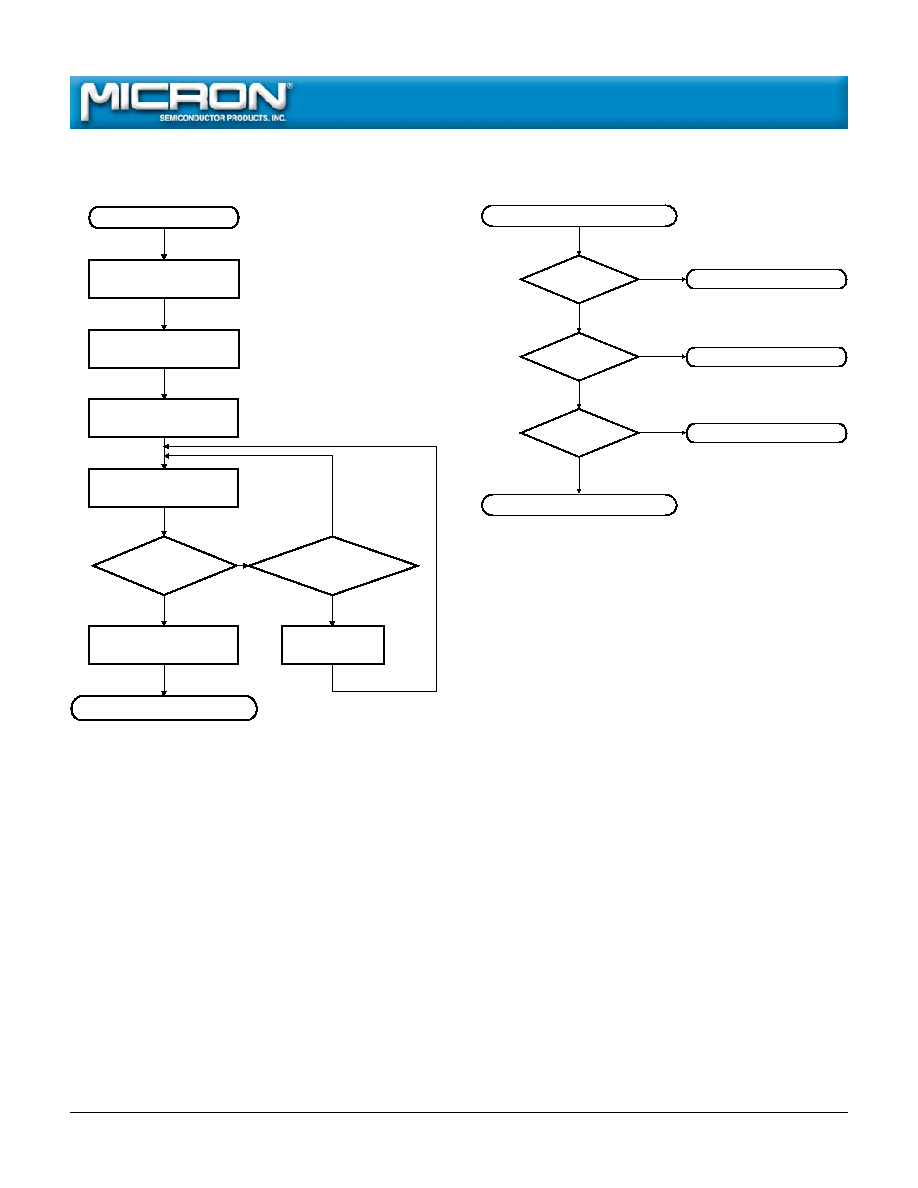
PP
voltage detected
continuously, nor does it indicate a valid V
PP
voltage. The V
PP
pin is
0 = V
PP
present
sampled for 5V after WRITE or ERASE CONFIRM is given. V
PP
S must be
cleared by CLEAR STATUS REGISTER or by a RESET.
SR0-2
RESERVED
Reserved for future use.
12
2Mb Smart 5 Boot Block Flash Memory
Micron Technology, Inc., reserves the right to change products or specifications without notice.
F50.p65 ≠ Rev. 1/00
©2000, Micron Technology, Inc.
2Mb
SMART 5 BOOT BLOCK FLASH MEMORY
COMMAND EXECUTION
Commands are issued to bring the device into differ-
ent operational modes. Each mode allows specific op-
erations to be performed. Several modes require a
sequence of commands to be written before they are
reached. The following section describes the properties
of each mode, and Table 3 lists all command sequences
required to perform the desired operation.
READ ARRAY
The array read mode is the initial state of the device
upon power-up and after a RESET. If the device is in any
other mode, READ ARRAY (FFH) must be given to
return to the array read mode. Unlike the WRITE SETUP
command (40H), READ ARRAY does not need to be
given before each individual read access.
IDENTIFY DEVICE
IDENTIFY DEVICE (90H) may be written to the CEL
to enter the identify device mode. While the device is
in this mode, any READ will produce the device ID
when A0 is HIGH and manufacturer compatibility ID
when A0 is LOW. The device will remain in this mode
until another command is given.
Table 3
Command Sequences
BUS
1ST
2ND
CYCLES
CYCLE
CYCLE
COMMANDS
REQ'D OPERATION ADDRESS DATA OPERATION ADDRESS DATA
NOTES
READ ARRAY
1
WRITE
X
FFH
1
IDENTIFY DEVICE
3
WRITE
X
90H
READ
IA
ID
2, 3
READ STATUS REGISTER
2
WRITE
X
70H
READ
X
SRD
4
CLEAR STATUS REGISTER
1
WRITE
X
50H
ERASE SETUP/CONFIRM
2
WRITE
X
20H
WRITE
BA
D0H
5, 6
ERASE SUSPEND/RESUME
2
WRITE
X
B0H
WRITE
X
D0H
WRITE SETUP/WRITE
2
WRITE
X
40H
WRITE
WA
WD
6, 7
ALTERNATE WORD/BYTE
2
WRITE
X
10H
WRITE
WA
WD
6, 7
WRITE
NOTE: 1. Must follow WRITE or ERASE CONFIRM commands to the CEL in order to enable flash array READ cycles.
2. IA = Identify Address: 00H for manufacturer compatibility ID; 01H for device ID.
3. ID = Identify Data.
4. SRD = Status Register Data.
5. On x16 (X00) devices BA = Block Address (A12-A16), on x8 (00X) devices BA = Block Address (A13-A17).
6. Addresses are "Don't Care" in first cycle but must be held stable.
7. WA = Address to be written; WD = Data to be written to WA.
WRITE SEQUENCE
Two consecutive cycles are needed to write data to
the array. WRITE SETUP (40H or 10H) is given in the
first cycle. The next cycle is the WRITE, during which
the write address and data are issued and V
PP
is brought
to V
PPH
. Writing to the boot block also requires that the
RP# pin be brought to V
HH
or that the WP# pin be
brought HIGH at the same time V
PP
is brought to V
PPH
.
The ISM will now begin to write the word or byte. V
PP
must be held at V
PPH
until the WRITE is completed
(SR7 = 1).
While the ISM executes the WRITE, the ISM status
bit (SR7) will be at "0," and the device will not respond
to any commands. Any READ operation will produce
the status register contents on DQ0-DQ7. When the
ISM status bit (SR7) is set to a logic 1, the WRITE has
been completed, and the device will go into the status
register read mode until another command is given.
After the ISM has initiated the WRITE, it cannot be
aborted except by a RESET or by powering down the
part. Doing either during a WRITE will corrupt the data
being written. If only the WRITE SETUP command has
been given, the WRITE may be nullified by performing
13
2Mb Smart 5 Boot Block Flash Memory
Micron Technology, Inc., reserves the right to change products or specifications without notice.
F50.p65 ≠ Rev. 1/00
©2000, Micron Technology, Inc.
2Mb
SMART 5 BOOT BLOCK FLASH MEMORY
a null WRITE. To execute a null WRITE, FFH must be
written when BYTE# is LOW, or FFFFH must be written
when BYTE# is HIGH. Once the ISM status bit (SR7) has
been set, the device will be in the status register read
mode until another command is issued.
ERASE SEQUENCE
Executing an ERASE sequence will set all bits within
a block to logic 1. The command sequence necessary to
execute an ERASE is similar to that of a WRITE. To
provide added security against accidental block era-
sure, two consecutive command cycles are required to
initiate an ERASE of a block. In the first cycle, addresses
are "Don't Care," and ERASE SETUP (20H) is given. In
the second cycle, V
PP
must be brought to V
PPH
, an
address within the block to be erased must be issued,
and ERASE CONFIRM (D0H) must be given. If a com-
mand other than ERASE CONFIRM is given, the write
and erase status bits (SR4 and SR5) will be set, and the
device will be in the status register read mode.
After the ERASE CONFIRM (D0H) is issued, the ISM
will start the ERASE of the addressed block. Any READ
operation will output the status register contents on
DQ0-DQ7. V
PP
must be held at V
PPH
until the ERASE is
completed (SR7 = 1). Once the ERASE is completed, the
device will be in the status register read mode until
another command is issued. Erasing the boot block also
requires that either the RP# pin be set to V
HH
or the WP#
pin be held HIGH at the same time V
PP
is set to V
PPH
.
ERASE SUSPENSION
The only command that may be issued while an
ERASE is in progress is ERASE SUSPEND. This command
allows other commands to be executed while pausing
the ERASE in progress. Once the device has reached the
erase suspend mode, the erase suspend status bit (SR6)
and ISM status bit (SR7) will be set. The device may now
be given a READ ARRAY, ERASE RESUME or READ
STATUS REGISTER command. After READ ARRAY has
been issued, any location not within the block being
erased may be read. If ERASE RESUME is issued before
SR6 has been set, the device will immediately proceed
with the ERASE in progress.
ERROR HANDLING
After the ISM status bit (SR7) has been set, the V
PP
(SR3), write (SR4) and erase (SR5) status bits may be
checked. If one or a combination of these three bits has
been set, an error has occurred. The ISM cannot reset
these three bits. To clear these bits, CLEAR STATUS
REGISTER (50H) must be given. If the V
PP
status bit
(SR3) is set, further WRITE or ERASE operations cannot
resume until the status register is cleared. Table 4 lists
the combination of errors.
Table 4
Status Register Error Decode
1
STATUS BITS
SR5
SR4
SR3
ERROR DESCRIPTION
0
0
0
No errors
0
0
1
V
PP
voltage error
0
1
0
WRITE error
0
1
1
WRITE error, V
PP
voltage not valid at time of WRITE
1
0
0
ERASE error
1
0
1
ERASE error, V
PP
voltage not valid at time of ERASE CONFIRM
1
1
0
Command sequencing error or WRITE/ERASE error
1
1
1
Command sequencing error, V
PP
voltage error, with WRITE and ERASE errors
NOTE: 1. SR3-SR5 must be cleared using CLEAR STATUS REGISTER.
14
2Mb Smart 5 Boot Block Flash Memory
Micron Technology, Inc., reserves the right to change products or specifications without notice.
F50.p65 ≠ Rev. 1/00
©2000, Micron Technology, Inc.
2Mb
SMART 5 BOOT BLOCK FLASH MEMORY
WRITE/ERASE CYCLE ENDURANCE
The MT28F002B5 and MT28F200B5 are designed
and fabricated to meet advanced firmware storage re-
quirements. To ensure this level of reliability, V
PP
must
be at 5V
±
10% during WRITE or ERASE cycles. Due to
process technology advances, 5V V
PP
is optimal for
application and production programming. For back-
ward compatibility with SmartVoltage technology, 12V
V
PP
is supported for a maximum of 100 cycles and may
be connected for up to 100 cumulative hours. Opera-
tion outside these limits may reduce the number of
WRITE and ERASE cycles that can be performed on the
device.
POWER USAGE
The MT28F002B5 and MT28F200B5 offer several
power-saving features that may be utilized in the array
read mode to conserve power. Deep power-down mode
is enabled by bringing RP# LOW. Current draw (I
CC
) in
this mode is a maximum of 20
µ
A at 5V V
CC
. When CE#
is HIGH, the device will enter standby mode. In this
mode, maximum I
CC
current is 130
µ
A at 5V. If CE# is
brought HIGH during a WRITE or ERASE, the ISM will
continue to operate, and the device will consume the
respective active power until the WRITE or ERASE is
completed.
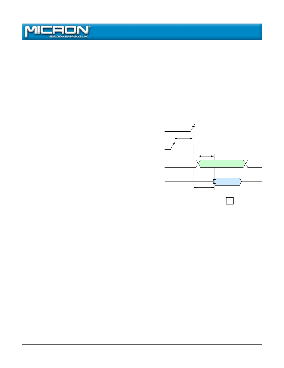
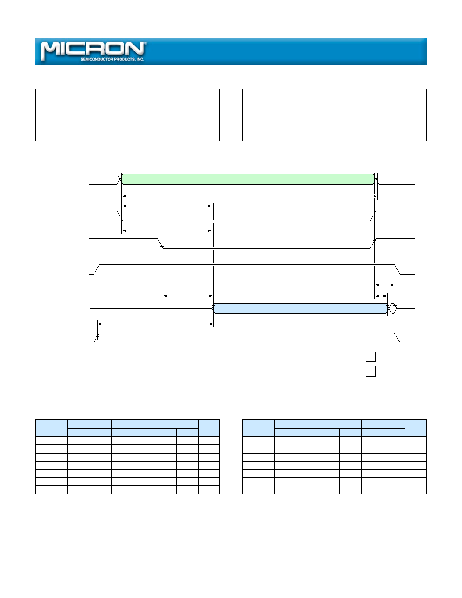
POWER-UP
The likelihood of unwanted WRITE or ERASE opera-
tions is minimized since two consecutive cycles are
required to execute either operation. However, to reset
the ISM and to provide additional protection while V
CC
is ramping, one of the following conditions must be
met:
∑ RP# must be held LOW until V
CC
is at valid
functional level; or
∑ CE# or WE# may be held HIGH and
RP# must be toggled from V
CC
-GND-V
CC
.
After a power-up or RESET, the status register is reset,
and the device will enter the array read mode.
Figure 2
Power-Up/Reset Timing Diagram
VALID
,,,
,,,
,,
VALID
V
CC
(5V)
Data
Address
UNDEFINED
,,
t
Note 1
RP#
RWH
t
AA
NOTE:
1. V
CC
must be within the valid operating range before RP#
goes HIGH.

15
2Mb Smart 5 Boot Block Flash Memory
Micron Technology, Inc., reserves the right to change products or specifications without notice.
F50.p65 ≠ Rev. 1/00
©2000, Micron Technology, Inc.
2Mb
SMART 5 BOOT BLOCK FLASH MEMORY
YES
NO
WRITE 40H or 10H
V
PP
= 5V
Start
WRITE Word or Byte
Address/Data
STATUS REGISTER
READ
SR7 = 1?
Complete Status
Check (optional)
WRITE Complete
3
2
NO
Start (WRITE completed)
YES
SR4 = 0?
SR3 = 0?
NO
YES
BYTE/WORD WRITE Error
5
WRITE Successful
V Error
PP
4, 5
COMPLETE WRITE STATUS-CHECK
SEQUENCE
SELF-TIMED WRITE SEQUENCE
(WORD or BYTE WRITE)
1
NOTE: 1. Sequence may be repeated for additional BYTE or WORD WRITEs.
2. Complete status check is not required. However, if SR3 = 1, further WRITEs are inhibited until the status register is
cleared.
3. Device will be in status register read mode. To return to the array read mode, the FFH command must be issued.
4. If SR3 is set during a WRITE or BLOCK ERASE attempt, CLEAR STATUS REGISTER must be issued before further WRITE
or ERASE operations are allowed by the CEL.
5. Status register bits 3-5 must be cleared using CLEAR STATUS REGISTER.
16
2Mb Smart 5 Boot Block Flash Memory
Micron Technology, Inc., reserves the right to change products or specifications without notice.
F50.p65 ≠ Rev. 1/00
©2000, Micron Technology, Inc.
2Mb
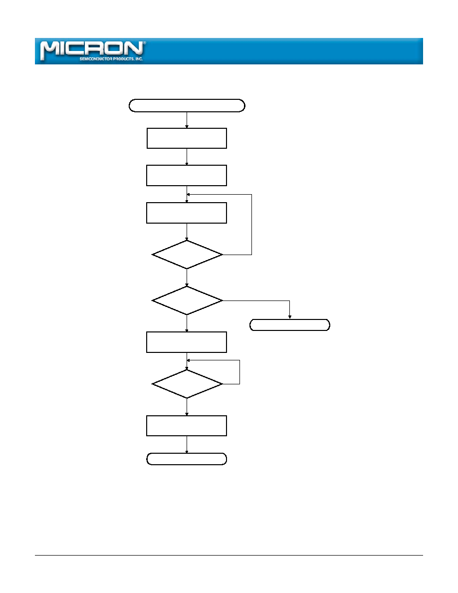
SMART 5 BOOT BLOCK FLASH MEMORY
NO
Start (ERASE completed)
YES
SR4, 5 = 1?
SR3 = 0?
YES
YES
Command Sequence Error
SR5 = 0?
NO
NO
6
V Error
PP
BLOCK ERASE Error
5, 6
6
ERASE Successful
YES
NO
V
PP
= 5V
Complete Status
Check (optional)
ERASE Complete
NO
YES
Suspend ERASE?
STATUS REGISTER
READ
SR7 = 1?
WRITE 20H
Start
WRITE D0H,
Block Address
Suspend
Sequence
ERASE Resumed
ERASE
Busy
3
4
2
SELF-TIMED BLOCK ERASE SEQUENCE
1
COMPLETE BLOCK ERASE
STATUS-CHECK SEQUENCE
NOTE: 1. Sequence may be repeated to erase additional blocks.
2. Complete status check is not required. However, if SR3 = 1, further ERASEs are inhibited until the status register is
cleared.
3. To return to the array read mode, the FFH command must be issued.
4. Refer to the ERASE SUSPEND flowchart for more information.
5. If SR3 is set during a WRITE or BLOCK ERASE attempt, CLEAR STATUS REGISTER must be issued before further WRITE
or ERASE operations are allowed by the CEL.
6. Status register bits 3-5 must be cleared using CLEAR STATUS REGISTER.
17
2Mb Smart 5 Boot Block Flash Memory
Micron Technology, Inc., reserves the right to change products or specifications without notice.
F50.p65 ≠ Rev. 1/00
©2000, Micron Technology, Inc.
2Mb
SMART 5 BOOT BLOCK FLASH MEMORY
ERASE SUSPEND/RESUME SEQUENCE
NO
WRITE B0H
(ERASE SUSPEND)
Start (ERASE in progress)
WRITE FFH
(READ ARRAY)
STATUS REGISTER
READ
YES
SR6 = 1?
SR7 = 1?
NO
YES
NO
YES
Done
Reading?
WRITE D0H
(ERASE RESUME)
Resume ERASE
ERASE Completed
V
PP
= 5V
18
2Mb Smart 5 Boot Block Flash Memory
Micron Technology, Inc., reserves the right to change products or specifications without notice.
F50.p65 ≠ Rev. 1/00
©2000, Micron Technology, Inc.
2Mb
SMART 5 BOOT BLOCK FLASH MEMORY
ABSOLUTE MAXIMUM RATINGS*
Voltage on V
CC
Supply
Relative to V
SS
................................ -0.5V to +6V**
Input Voltage Relative to V
SS
................ -0.5V to +6V**
V
PP
Voltage Relative to V
SS
............... -0.5V to +12.6V
RP# or A9 Pin Voltage
Relative to V
SS
............................ -0.5V to +12.6V
Temperature Under Bias ...................... -40
∞
C to +85
∞
C
Storage Temperature (plastic) ............ -55
∞
C to +125
∞
C
Power Dissipation ................................................... 1W
*Stresses greater than those listed under "Absolute
Maximum Ratings" may cause permanent damage to
the device. This is a stress rating only, and functional
operation of the device at these or any other conditions
above those indicated in the operational sections of
this specification is not implied. Exposure to absolute
maximum rating conditions for extended periods may
affect reliability.
**V
CC
, input and I/O pins may transition to -2V for
<20ns and V
CC
+ 2V for <20ns.
Voltage may pulse to -2V for <20ns and 14V for <20ns.
ELECTRICAL CHARACTERISTICS AND RECOMMENDED DC READ
OPERATING CONDITIONS
Commercial Temperature (0
∞
C
T
A
+70
∞
C) and Extended Temperature (-40
∞
C
T
A
+85
∞
C)
PARAMETER/CONDITION
SYMBOL
MIN
MAX
UNITS
NOTES
5V Supply Voltage
V
CC
4.5
5.5
V
1
Input High (Logic 1) Voltage, all inputs
V
IH
2
V
CC
+ 0.5
V
1
Input Low (Logic 0) Voltage, all inputs
V
IL
-0.5
0.8
V
1
Device Identification Voltage, A9
V
ID
11.4
12.6
V
1
V
PP
Supply Voltage
V
PP
-0.5
12.6
V
1
DC OPERATING CHARACTERISTICS
Commercial Temperature (0
∞
C
T
A
+70
∞
C) and Extended Temperature (-40
∞
C
T
A
+85
∞
C)
PARAMETER/CONDITION
SYMBOL
MIN
MAX
UNITS NOTES
OUTPUT VOLTAGE LEVELS (TTL)
V
OH
1
2.4
≠
V
Output High Voltage (I
OH
= -2.5mA)
1
Output Low Voltage (I
OL
= 5.8mA)
V
OL
≠
0.45
V
OUTPUT VOLTAGE LEVELS (CMOS)
V
OH
2
V
CC
- 0.4
≠
V
1
Output High Voltage (I
OH
= -100
µ
A)
INPUT LEAKAGE CURRENT
Any input (0V
V
IN
V
CC
);
I
L
-1
1
µ
A
All other pins not under test = 0V
INPUT LEAKAGE CURRENT: A9 INPUT
I
ID
≠
500
µ
A
(11.4V
A9
12.6 = V
ID
)
INPUT LEAKAGE CURRENT: RP# INPUT
I
HH
≠
500
µ
A
(11.4V
RP#
12.6 = V
HH
)
OUTPUT LEAKAGE CURRENT
I
OZ
-10
10
µ
A
(D
OUT
is disabled; 0V
V
OUT
V
CC
)
NOTE: 1. All voltages referenced to V
SS
.
19
2Mb Smart 5 Boot Block Flash Memory
Micron Technology, Inc., reserves the right to change products or specifications without notice.
F50.p65 ≠ Rev. 1/00
©2000, Micron Technology, Inc.
2Mb
SMART 5 BOOT BLOCK FLASH MEMORY
READ AND STANDBY CURRENT DRAIN
Commercial Temperature (0
∞
C
T
A
+70
∞
C) and Extended Temperature (-40
∞
C
T
A
+85
∞
C)
PARAMETER/CONDITION
SYMBOL
MAX
UNITS
NOTES
READ CURRENT: WORD-WIDE, TTL INPUT LEVELS
I
CC
1
55
mA
1, 2
(CE# = V
IL
; OE# = V
IH
; f =
10 MHz; Other inputs = V
IL
or V
IH
; RP# = V
IH
)
READ CURRENT: WORD-WIDE, CMOS INPUT LEVELS
(CE#
0.2V; OE#
V
CC
- 0.2V; f =
10 MHz; Other inputs
0.2V
I
CC
2
50
mA
1, 2
or
V
CC
- 0.2V; RP#
V
CC
- 0.2V)
READ CURRENT: BYTE-WIDE, TTL INPUT LEVELS
I
CC
3
55
mA
1, 2
(CE# = V
IL
; OE# = V
IH
; f =
10 MHz; Other inputs = V
IL
or V
IH
; RP# = V
IH
)
READ CURRENT: BYTE-WIDE, CMOS INPUT LEVELS
(CE#
0.2V; OE#
V
CC
- 0.2V; f =
10 MHz; Other inputs
0.2V
I
CC
4
50
mA
1, 2
or
V
CC
- 0.2V; RP# = V
CC
- 0.2V)
STANDBY CURRENT: TTL INPUT LEVELS
V
CC
power supply standby current
I
CC
5
2
mA
(CE# = RP# = V
IH
; Other inputs = V
IL
or V
IH
)
STANDBY CURRENT: CMOS INPUT LEVELS
V
CC
power supply standby current
I
CC
6
130
µ
A
(CE# = RP# = V
CC
- 0.2V)
DEEP POWER-DOWN CURRENT: V
CC
SUPPLY (RP# = V
SS
±
0.2V)
I
CC
8
20
µ
A
STANDBY OR READ CURRENT: V
PP
SUPPLY (V
PP
5.5V)
I
PP
1
±
15
µ
A
DEEP POWER-DOWN CURRENT: V
PP
SUPPLY (RP# = V
SS
±
0.2V)
I
PP
2
5
µ
A
CAPACITANCE
(T
A
= +25
∞
C; f = 1 MHz)
PARAMETER/CONDITION
SYMBOL
MAX
UNITS
NOTES
Input Capacitance
C
I
8
pF
Output Capacitance
C
O
12
pF
NOTE: 1. I
CC
is dependent on cycle rates.
2. I
CC
is dependent on output loading. Specified values are obtained with the outputs open.
20
2Mb Smart 5 Boot Block Flash Memory
Micron Technology, Inc., reserves the right to change products or specifications without notice.
F50.p65 ≠ Rev. 1/00
©2000, Micron Technology, Inc.
2Mb
SMART 5 BOOT BLOCK FLASH MEMORY
READ TIMING PARAMETERS
ELECTRICAL CHARACTERISTICS AND RECOMMENDED AC OPERATING CONDITIONS
TEST CONDITION 1
Commercial Temperature (0
∞
C
T
A
+70
∞
C) and Extended Temperature (-40
∞
C
T
A
+85
∞
C); V
CC
= +5V
±
10%
AC CHARACTERISTICS
-6
-8
-8 ET
PARAMETER
SYMBOL
MIN
MAX
MIN
MAX
MIN
MAX UNITS NOTES
READ cycle time
t
RC
70
80
80
ns
Access time from CE#
t
ACE
70
80
80
ns
1
Access time from OE#
t
AOE
35
40
40
ns
1
Access time from address
t
AA
70
80
80
ns
RP# HIGH to output valid delay
t
RWH
500
500
500
ns
OE# or CE# HIGH to output in High-Z
t
OD
20
20
20
ns
Output hold time from OE#, CE# or address change
t
OH
0
0
0
ns
RP# LOW pulse width
t
RP
60
60
60
ns
TEST CONDITION 2
(0
∞
C
T
A
+70
∞
C; V
CC
= +5V
±
5%)
AC CHARACTERISTICS
-6
PARAMETER
SYMBOL
MIN
MAX
UNITS NOTES
READ cycle time
t
RC
60
ns
Access time from CE#
t
ACE
60
ns
1
Access time from OE#
t
AOE
30
ns
1
Access time from address
t
AA
60
ns
RP# HIGH to output valid delay
t
RWH
500
ns
OE# or CE# HIGH to output in High-Z
t
OD
15
ns
Output hold time from OE#, CE# or address change
t
OH
0
ns
RP# LOW pulse width
t
RP
60
ns
NOTE: 1. OE# may be delayed by
t
ACE minus
t
AOE after CE# falls before
t
ACE is affected.
21
2Mb Smart 5 Boot Block Flash Memory
Micron Technology, Inc., reserves the right to change products or specifications without notice.
F50.p65 ≠ Rev. 1/00
©2000, Micron Technology, Inc.
2Mb
SMART 5 BOOT BLOCK FLASH MEMORY
TIMING PARAMETERS
Commercial Temperature (0
∞
C
T
A
+70
∞
C)
Extended Temperature (-40
∞
C
T
A
+85
∞
C)
-6
-8
-8 ET
SYMBOL
MIN
MAX
MIN
MAX
MIN
MAX
UNITS
t
RC
3
70
80
80
ns
t
RC
4
60
≠
≠
ns
t
ACE
3
70
80
80
ns
t
ACE
4
60
≠
≠
ns
t
AOE
3
35
40
40
ns
t
AOE
4
30
≠
≠
ns
t
AA
3
70
80
80
ns
AC TEST CONDITION 1
Input pulse levels ............................................... 0.4V to 2.4V
Input rise and fall times ................................................ <10ns
Input timing reference level ............................... 0.8V and 2V
Output timing reference level ........................... 0.8V and 2V
Output load ................................. 1 TTL gate and C
L
= 100pF
AC TEST CONDITION 2
Input pulse levels ..................................................... 0V to 3V
Input rise and fall times ................................................ <10ns
Input timing reference level ........................................... 1.5V
Output timing reference level ....................................... 1.5V
Output load ................................... 1 TTL gate and C
L
= 50pF
WORD-WIDE READ CYCLE
1, 2
,,
,,
,,
VALID DATA
VALID ADDRESS
CE#
A0-A16/(A17)
OE#
DQ0-DQ15
tRC
tACE
tAOE
tOD
tOH
tAA
,,
WE#
RP#
V
IH
V
IL
V
IH
V
IL
V
IH
V
IL
V
IH
V
IL
V
IH
V
IL
V
IH
V
IL
tRWH
DON'T CARE
UNDEFINED
,,
,
,
NOTE: 1. BYTE# = HIGH (MT28F200B5 only).
2. Applies to MT28F200B5 only.
3. Measurements tested under AC Test Condition 1, V
CC
= 5V
±
10%.
4. Measurements tested under AC Test Condition 2, V
CC
= 5V
±
5%.
-6
-8
-8 ET
SYMBOL
MIN
MAX
MIN
MAX
MIN
MAX
UNITS
t
AA
4
60
≠
≠
ns
t
RWH
3
500
500
500
ns
t
RWH
4
500
≠
≠
ns
t
OD
3
20
20
20
ns
t
OD
4
15
≠
≠
ns
t
OH
3
0
0
0
ns
t
OH
4
0
≠
≠
ns
22
2Mb Smart 5 Boot Block Flash Memory
Micron Technology, Inc., reserves the right to change products or specifications without notice.
F50.p65 ≠ Rev. 1/00
©2000, Micron Technology, Inc.
2Mb
SMART 5 BOOT BLOCK FLASH MEMORY
BYTE-WIDE READ CYCLE
1
,,,
,,
,,,
VALID DATA
VALID ADDRESS
CE#
(A - 1)-A16/(A17)
1
OE#
DQ0-DQ7
DON'T CARE
UNDEFINED
,,
,
,
tRC
tACE
tAOE
tOD
tOH
tAA
,
WE#
RP#
V
IH
V
IL
V
IH
V
IL
V
IH
V
IL
V
IH
V
IL
V
IH
V
IL
V
IH
V
IL
tRWH
DQ8-DQ14
2
V
IH
V
IL
HIGH-Z
NOTE: 1. BYTE# = LOW (MT28F200B5 only).
2. Applies to MT28F200B5 only.
3. Measurements tested under AC Test Condition 1, V
CC
= 5V
±
10%.
4. Measurements tested under AC Test Condition 2, V
CC
= 5V
±
5%.
TIMING PARAMETERS
Commercial Temperature (0
∞
C
T
A
+70
∞
C)
Extended Temperature (-40
∞
C
T
A
+85
∞
C)
-6
-8
-8 ET
SYMBOL
MIN
MAX
MIN
MAX
MIN
MAX
UNITS
t
RC
3
70
80
80
ns
t
RC
4
60
≠
≠
ns
t
ACE
3
70
80
80
ns
t
ACE
4
60
≠
≠
ns
t
AOE
3
35
40
40
ns
t
AOE
4
30
≠
≠
ns
t
AA
3
70
80
80
ns
-6
-8
-8 ET
SYMBOL
MIN
MAX
MIN
MAX
MIN
MAX
UNITS
t
AA
4
60
≠
≠
ns
t
RWH
3
500
500
500
ns
t
RWH
4
500
≠
≠
ns
t
OD
3
20
20
20
ns
t
OD
4
15
≠
≠
ns
t
OH
3
0
0
0
ns
t
OH
4
0
≠
≠
ns
23
2Mb Smart 5 Boot Block Flash Memory
Micron Technology, Inc., reserves the right to change products or specifications without notice.
F50.p65 ≠ Rev. 1/00
©2000, Micron Technology, Inc.
2Mb
SMART 5 BOOT BLOCK FLASH MEMORY
WRITE/ERASE CURRENT DRAIN
Commercial Temperature (0
∞
C
T
A
+70
∞
C) and Extended Temperature (-40
∞
C
T
A
+85
∞
C); V
CC
= +5V
±
10%
PARAMETER/CONDITION
SYMBOL
MIN
UNITS NOTES
WORD WRITE CURRENT: V
CC
SUPPLY
I
CC
9
25
mA
5
WORD WRITE CURRENT: V
PP
SUPPLY
I
PP
4
20
mA
5
BYTE WRITE CURRENT: V
CC
SUPPLY
I
CC
10
25
mA
6
BYTE WRITE CURRENT: V
PP
SUPPLY
I
PP
5
15
mA
6
ERASE CURRENT: V
CC
SUPPLY
I
CC
11
30
mA
ERASE CURRENT: V
PP
SUPPLY
I
PP
6
40
mA
ERASE SUSPEND CURRENT: V
CC
SUPPLY
I
CC
12
10
mA
7
(ERASE suspended)
ERASE SUSPEND CURRENT: V
PP
SUPPLY
I
PP
7
200
µ
A
(ERASE suspended)
RECOMMENDED DC WRITE/ERASE CONDITIONS
1
Commercial Temperature (0
∞
C
T
A
+70
∞
C) and Extended Temperature (-40
∞
C
T
A
+85
∞
C); V
CC
= +5V
±
10%
PARAMETER/CONDITION
SYMBOL
MIN
MAX
UNITS NOTES
V
PP
WRITE/ERASE lockout voltage
V
PPLK
≠
1.5
V
2
V
PP
voltage during WRITE/ERASE operation
V
PPH
1
4.5
5.5
V
3
V
PP
voltage during WRITE/ERASE operation
V
PPH
2
11.4
12.6
V
4
Boot block unlock voltage
V
HH
11.4
12.6
V
V
CC
WRITE/ERASE lockout voltage
V
LKO
2
≠
V
NOTE: 1. WRITE operations are tested at V
CC
/V
PP
voltages equal to or less than the previous ERASE, and READ operations are
tested at V
CC
voltages equal to or less than the previous WRITE.
2. Absolute WRITE/ERASE protection when V
PP
V
PPLK
.
3. When 5V V
CC
and V
PP
are used, V
CC
cannot exceed V
PP
by more than 500mV during WRITE and ERASE operations.
4. For SmartVoltage-compatible production programming, 12V V
PP
is supported for a maximum of 100 cycles and may
be connected for up to 100 cummulative hours.
5. Applies to MT28F200B5 only.
6. Applies to MT28F002B5 and MT28F200B5 with BYTE = LOW.
7. Parameter is specified when device is not accessed. Actual current draw will be I
CC
12
(5V V
CC
) plus read current if a
READ is executed while the device is in erase suspend mode.
24
2Mb Smart 5 Boot Block Flash Memory
Micron Technology, Inc., reserves the right to change products or specifications without notice.
F50.p65 ≠ Rev. 1/00
©2000, Micron Technology, Inc.
2Mb
SMART 5 BOOT BLOCK FLASH MEMORY
SPEED-DEPENDENT WRITE/ERASE AC TIMING CHARACTERISTICS AND
RECOMMENDED AC OPERATING CONDITIONS
TEST CONDITION 1
Commercial Temperature (0
∞
C
T
A
+70
∞
C) and Extended Temperature (-40
∞
C
T
A
+85
∞
C); V
CC
= +5V
±
10%
AC CHARACTERISTICS
-6
-8/-8 ET
PARAMETER
SYMBOL
MIN
MAX
MIN
MAX
UNITS
NOTES
WRITE cycle time
t
WC
70
80
ns
WE# HIGH pulse width
t
WPH
20
30
ns
CE# HIGH pulse width
t
CPH
20
30
ns
CE# pulse width
t
CP
50
50
ns
WE# pulse width
t
WP
50
50
ns
TEST CONDITION 2
(0
∞
C
T
A
+70
∞
C; V
CC
= +5V
±
5%)
AC CHARACTERISTICS
-6
PARAMETER
SYMBOL
MIN
MAX
UNITS
NOTES
WRITE cycle time
t
WC
60
ns
WE# HIGH pulse width
t
WPH
20
ns
CE# HIGH pulse width
t
CPH
20
ns
CE# pulse width
t
CP
50
ns
WE# pulse width
t
WP
50
ns

25
2Mb Smart 5 Boot Block Flash Memory
Micron Technology, Inc., reserves the right to change products or specifications without notice.
F50.p65 ≠ Rev. 1/00
©2000, Micron Technology, Inc.
2Mb
SMART 5 BOOT BLOCK FLASH MEMORY
SPEED-DEPENDENT WRITE/ERASE AC TIMING CHARACTERISTICS AND RECOM-
MENDED AC OPERATING CONDITIONS: WE#-CONTROLLED WRITES
Commercial Temperature (0
∞
C
T
A
+70
∞
C) and Extended Temperature (-40
∞
C
T
A
+85
∞
C); V
CC
= +5V
±
10% or
+5V
±
5%
AC CHARACTERISTICS
-6/-8/-8 ET
PARAMETER
SYMBOL
MIN
MAX
UNITS
NOTES
Address setup time to WE# HIGH
t
AS
50
ns
Address hold time from WE# HIGH
t
AH
0
ns
Data setup time to WE# HIGH
t
DS
50
ns
Data hold time from WE# HIGH
t
DH
0
ns
CE# setup time to WE# LOW
t
CS
0
ns
CE# hold time from WE# HIGH
t
CH
0
ns
V
PP
setup time to WE# HIGH
t
VPS1
200
ns
1
RP# HIGH to WE# LOW delay
t
RS
500
ns
RP# at V
HH
or WP# HIGH setup time to WE# HIGH
t
RHS
100
ns
2
WRITE duration (WORD or BYTE WRITE)
t
WED1
6
µ
s
3
Boot BLOCK ERASE duration
t
WED2
300
ms
2, 3
Parameter BLOCK ERASE duration
t
WED3
300
ms
3
Main BLOCK ERASE duration
t
WED4
600
ms
3
WE# HIGH to busy status (SR7 = 0)
t
WB
200
ns
4
V
PP
hold time from status data valid
t
VPH
0
ns
3
RP# at V
HH
or WP# HIGH hold time from status data valid
t
RHH
0
ns
2
Boot block relock delay time
t
REL
100
ns
5
NOTE: 1. Measured with V
PP
= V
PPH
1
= 5V.
2. RP# should be held at V
HH
or WP# held HIGH until boot block WRITE or ERASE is complete.
3. WRITE/ERASE times are measured to valid status register data (SR7 = 1).
4. Polling status register before
t
WB is met may falsely indicate WRITE or ERASE completion.
5.
t
REL is required to relock boot block after WRITE or ERASE to boot block.
26
2Mb Smart 5 Boot Block Flash Memory
Micron Technology, Inc., reserves the right to change products or specifications without notice.
F50.p65 ≠ Rev. 1/00
©2000, Micron Technology, Inc.
2Mb
SMART 5 BOOT BLOCK FLASH MEMORY
WORD/BYTE WRITE AND ERASE DURATION CHARACTERISTICS
PARAMETER
TYP MAX UNITS NOTES
Boot/parameter BLOCK ERASE time
0.5
7
s
6
Main BLOCK ERASE time
1.5
14
s
6
Main BLOCK WRITE time (byte mode)
1
≠
s
6, 7, 8
Main BLOCK WRITE time (word mode)
1
≠
s
6, 7, 8
SPEED-DEPENDENT WRITE/ERASE AC TIMING CHARACTERISTICS AND RECOM-
MENDED AC OPERATING CONDITIONS: CE#-CONTROLLED WRITES
Commercial Temperature (0
∞
C
T
A
+70
∞
C) and Extended Temperature (-40
∞
C
T
A
+85
∞
C); V
CC
= +5V
±
10% or
+5V
±
5%
AC CHARACTERISTICS
-6/-8/-8 ET
PARAMETER
SYMBOL
MIN
MAX
UNITS
NOTES
Address setup time to CE# HIGH
t
AS
50
ns
Address hold time from CE# HIGH
t
AH
0
ns
Data setup time to CE# HIGH
t
DS
50
ns
Data hold time from CE# HIGH
t
DH
0
ns
WE# setup time to CE# LOW
t
WS
0
ns
WE# hold time from CE# HIGH
t
WH
0
ns
V
PP
setup time to CE# HIGH
t
VPS1
200
ns
1
RP# HIGH to CE# LOW delay
t
RS
500
ns
RP# at V
HH
or WP# HIGH setup time to CE# HIGH
t
RHS
100
ns
2
WRITE duration (WORD or BYTE WRITE)
t
WED1
6
µ
s
3
Boot BLOCK ERASE duration
t
WED2
300
ms
2, 3
Parameter BLOCK ERASE duration
t
WED3
300
ms
3
Main BLOCK ERASE duration
t
WED4
600
ms
3
CE# HIGH to busy status (SR7 = 0)
t
WB
200
ns
4
V
PP
hold time from status data valid
t
VPH
0
ns
3
RP# at V
HH
or WP# HIGH hold time from status data valid
t
RHH
0
ns
2
Boot block relock delay time
t
REL
100
ns
5
NOTE: 1. Measured with V
PP
= V
PPH
1
= 5V.
2. RP# should be held at V
HH
or WP# held HIGH until boot block WRITE or ERASE is complete.
3. WRITE/ERASE times are measured to valid status register data (SR7 = 1).
4. Polling status register before
t
WB is met may falsely indicate WRITE or ERASE completion.
5.
t
REL is required to relock boot block after WRITE or ERASE to boot block.
6. Typical values measured at T
A
= +25
∞
C.
7. Assumes no system overhead.
8. Typical WRITE times use checkerboard data pattern.

27
2Mb Smart 5 Boot Block Flash Memory
Micron Technology, Inc., reserves the right to change products or specifications without notice.
F50.p65 ≠ Rev. 1/00
©2000, Micron Technology, Inc.
2Mb
SMART 5 BOOT BLOCK FLASH MEMORY
,,
,,,,
,,,
,,,
,,,
DON'T CARE
,
,,
tWC
tWED1/2/3/4
tRS
A
IN
Status
(SR7=1)
tCH
tCS
[Unlock boot block]
tRHS
tVPH
tAS
tAH
tWP
tWPH
tDS
tDH
CMD
in
tRHH
CMD/
Data-in
CMD
in
WRITE SETUP or
ERASE SETUP input
WRITE or ERASE (block)
address asserted, and
WRITE data or ERASE
CONFIRM issued
WRITE or ERASE
executed, status register
checked for completion
Command for next
operation issued
tDH
tDS
,
,,
,,
,
[Unlock boot block]
tVPS1
Note 1
tAS
tAH
Status
(SR7=0)
tWB
CE#
A0-A16/(A17)
OE#
DQ0-DQ7/
DQ0-DQ15
2
WE#
RP#
3
V
IH
V
IL
V
PP
V
HH
V
IH
V
IL
V
IH
V
IL
V
IH
V
IL
V
IH
V
IL
V
IH
V
IL
WP#
3
V
IH
V
IL
V
IL
V
PPH1
V
PPLK
[5V V
PP
]
,,
,,,
,,,,
,,,,
,,,
,,,
,,,
WRITE/ERASE CYCLE
WE#-CONTROLLED WRITE/ERASE
TIMING PARAMETERS
Commercial Temperature (0
∞
C
T
A
+70
∞
C)
Extended Temperature (-40
∞
C
T
A
+85
∞
C)
-6
-8/-8 ET
SYMBOL
MIN
MAX
MIN
MAX
UNITS
t
WC
4
70
80
ns
t
WC
5
60
≠
ns
t
WPH
4
20
30
ns
t
WPH
5
20
≠
ns
t
WP
4
50
50
ns
t
WP
5
50
≠
ns
t
AS
50
50
ns
t
AH
0
0
ns
t
DS
50
50
ns
t
DH
0
0
ns
t
CS
0
0
ns
-6
-8/-8 ET
SYMBOL
MIN
MAX
MIN
MAX
UNITS
NOTE: 1. Address inputs are "Don't Care" but must be held stable.
2. If BYTE# is LOW, data and command are 8-bit. If BYTE# is HIGH, data is 16-bit and command is 8-bit (MT28F200B5
only).
3. Either RP# at V
HH
or WP# HIGH unlocks the boot block.
4. Measurements tested under AC Test Condition 1, V
CC
= 5V
±
10%.
5. Measurements tested under AC Test Condition 2, V
CC
= 5V
±
5%.
t
CH
0
0
ns
t
VPS1
200
200
ns
t
RS
500
500
ns
t
RHS
100
100
ns
t
WED1
6
6
µ
s
t
WED2
300
300
ms
t
WED3
300
300
ms
t
WED4
600
600
ms
t
WB
200
200
ns
t
VPH
0
0
ns
t
RHH
0
0
ns
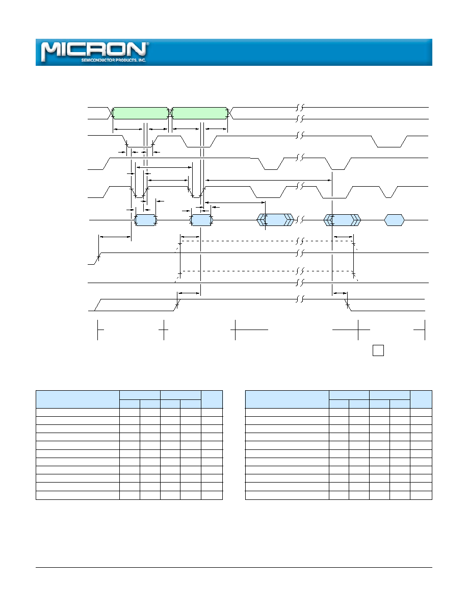
28
2Mb Smart 5 Boot Block Flash Memory
Micron Technology, Inc., reserves the right to change products or specifications without notice.
F50.p65 ≠ Rev. 1/00
©2000, Micron Technology, Inc.
2Mb
SMART 5 BOOT BLOCK FLASH MEMORY
,,
,,,,
,,,
,,,,
,,
DON'T CARE
,
,
tWC
tWED1/2/3/4
tRS
A
IN
Status
(SR7=1)
tWH
tWS
[Unlock boot block]
tRHS
tVPH
tAS
tAH
tCP
tCPH
tDS
tDH
CMD
in
tRHH
CMD/
Data-in
CMD
in
WRITE SETUP or
ERASE SETUP input
WRITE or ERASE (block)
address asserted, and
WRITE data or ERASE
CONFIRM issued
WRITE or ERASE
executed, status register
checked for completion
Command for next
operation issued
tDH
tDS
,
,
[5V V
PP
]
,,
[Unlock boot block]
tVPS1
Note 1
tAS
tAH
Status
(SR7=0)
tWB
WE#
A0-A16/(A17)
OE#
DQ0-DQ7/
DQ0-DQ15
2
CE#
RP#
3
V
IH
V
IL
V
PP
V
IH
V
IL
V
HH
V
IH
V
IL
V
IH
V
IL
V
IH
V
IL
V
IH
V
IL
WP#
3
V
IH
V
IL
V
IL
V
PPH1
V
PPLK
,,
,,,,
,,,,
,,,
,,,
,,,,
,,
WRITE/ERASE CYCLE
CE#-CONTROLLED WRITE/ERASE
t
WH
0
0
ns
t
VPS1
200
200
ns
t
RS
500
500
ns
t
RHS
100
100
ns
t
WED1
6
6
µ
s
t
WED2
300
300
ms
t
WED3
300
300
ms
t
WED4
600
600
ms
t
WB
200
200
ns
t
VPH
0
0
ns
t
RHH
0
0
ns
TIMING PARAMETERS
Commercial Temperature (0
∞
C
T
A
+70
∞
C)
Extended Temperature (-40
∞
C
T
A
+85
∞
C)
-6
-8/-8 ET
SYMBOL
MIN
MAX
MIN
MAX
UNITS
t
WC
4
70
80
ns
t
WC
5
60
≠
ns
t
CPH
4
20
30
ns
t
CPH
5
20
≠
ns
t
CP
4
50
50
ns
t
CP
5
50
≠
ns
t
AS
50
50
ns
t
AH
0
0
ns
t
DS
50
50
ns
t
DH
0
0
ns
t
WS
0
0
ns
-6
-8/-8 ET
SYMBOL
MIN
MAX
MIN
MAX
UNITS
NOTE: 1. Address inputs are "Don't Care" but must be held stable.
2. If BYTE# is LOW, data and command are 8-bit. If BYTE# is HIGH, data is 16-bit and command is 8-bit (MT28F200B5
only).
3. Either RP# at V
HH
or WP# HIGH unlocks the boot block.
4. Measurements tested under AC Test Condition 1, V
CC
= 5V
±
10%.
5. Measurements tested under AC Test Condition 2, V
CC
= 5V
±
5%.
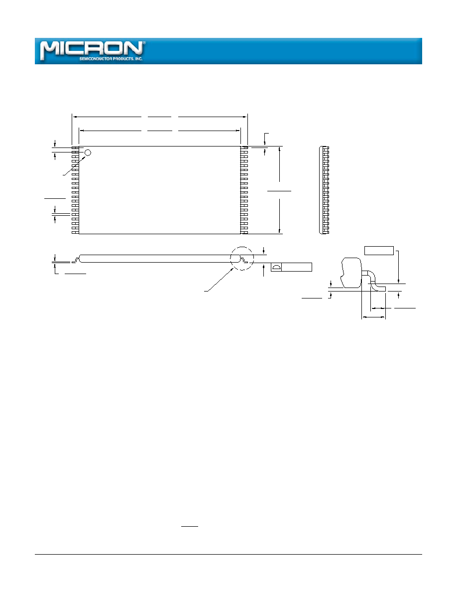
29
2Mb Smart 5 Boot Block Flash Memory
Micron Technology, Inc., reserves the right to change products or specifications without notice.
F50.p65 ≠ Rev. 1/00
©2000, Micron Technology, Inc.
2Mb
SMART 5 BOOT BLOCK FLASH MEMORY
40-PIN PLASTIC TSOP I
(10mm x 20mm)
DETAIL A
.721 (18.31)
.780 (19.81)
.397 (10.08)
.010 (0.25)
.0197 (0.50)
.010 (0.25)
.007 (0.18)
SEE DETAIL A
.795 (20.19)
.727 (18.47)
.006 (0.15)
TYP
.005 (0.13)
.391 (9.93)
.024 (0.60)
.016 (0.40)
.008 (0.20)
.004 (0.10)
.002 (0.05)
.0315 (0.80)
.047 (1.20)
MAX
40
1
20
21
.010 (0.25)
PLANE
GAGE
PIN #1 INDEX
NOTE: 1. All dimensions in inches (millimeters) MAX or typical where noted.
MIN
2. Package width and length do not include mold protrusion; allowable mold protrusion is .01" per side.
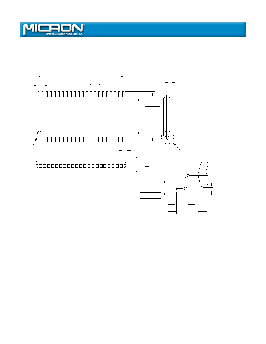
30
2Mb Smart 5 Boot Block Flash Memory
Micron Technology, Inc., reserves the right to change products or specifications without notice.
F50.p65 ≠ Rev. 1/00
©2000, Micron Technology, Inc.
2Mb
SMART 5 BOOT BLOCK FLASH MEMORY
44-PIN PLASTIC SOP
(600 mil)
.016 (0.40)
.010 (0.25)
.066 (1.72)
.020 (0.50)
.015 (0.38)
.007 (0.18)
.005 (0.13)
.004 (0.10)
.643 (16.34)
.620 (15.74)
DETAIL A
PIN #1 INDEX
(ROTATED 90
∞
CW)
SEE DETAIL A
GAGE PLANE
.0315 (0.80)
1.113 (28.27)
1.107 (28.12)
.010 (0.25)
.499 (12.68)
.493 (12.52)
.030 (0.76)
.106 (2.70) MAX
.050 (1.27)
TYP
NOTE: 1. All dimensions in inches (millimeters) MAX or typical where noted.
MIN
2. Package width and length do not include mold protrusion; allowable mold protrusion is .01" per side.
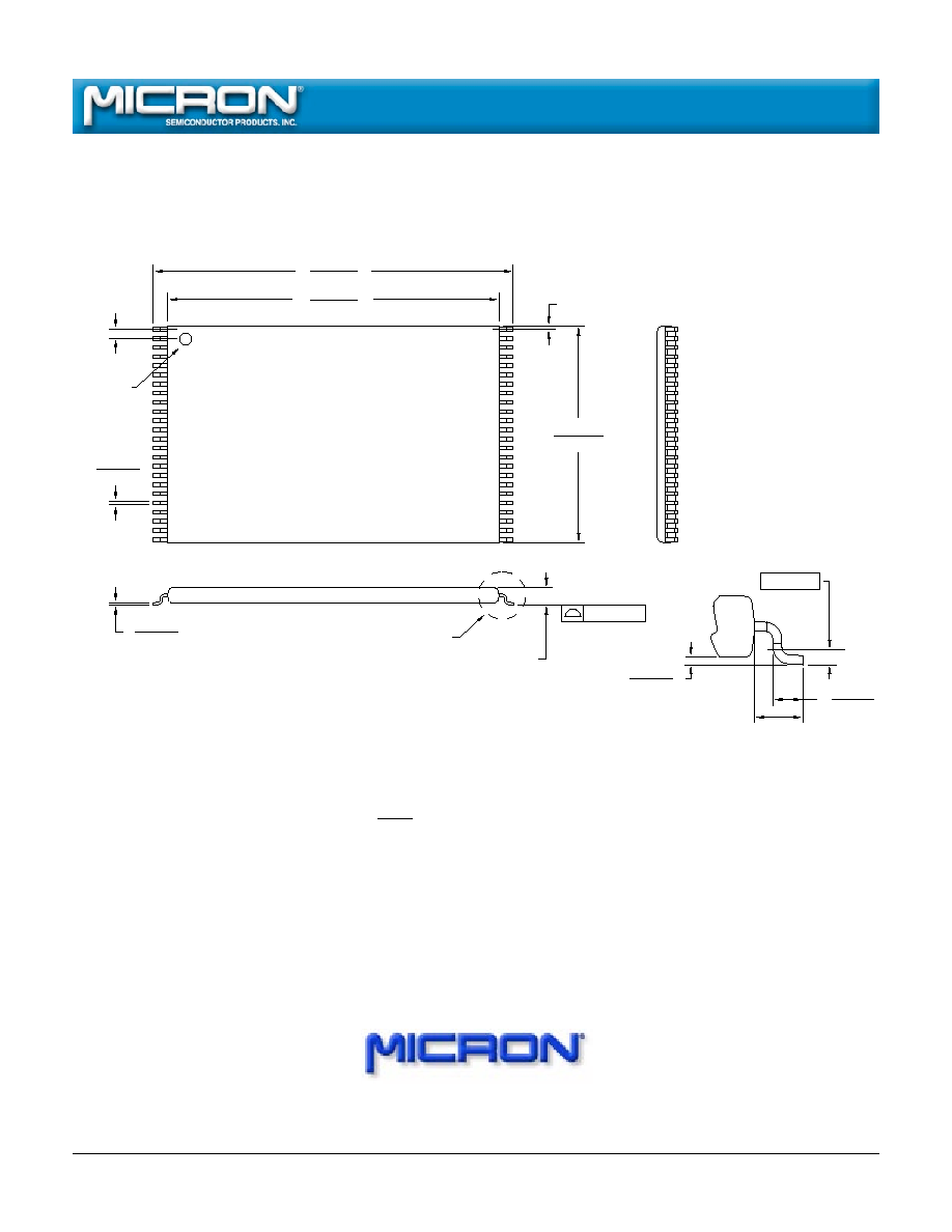
31
2Mb Smart 5 Boot Block Flash Memory
Micron Technology, Inc., reserves the right to change products or specifications without notice.
F50.p65 ≠ Rev. 1/00
©2000, Micron Technology, Inc.
2Mb
SMART 5 BOOT BLOCK FLASH MEMORY
48-PIN PLASTIC TSOP I
(12mm x 20mm)
.047 (1.20) MAX
.005 (0.12)
.007 (0.18)
24
.006 (0.15)
.010 (0.25)
SEE DETAIL A
.0197 (0.50)
TYP
1
.780 (19.81)
.727 (18.47)
.721 (18.31)
.795 (20.19)
.475 (12.07)
.002 (0.05)
DETAIL A
.016 (0.40)
.024 (0.60)
.0315 (0.80)
.008 (0.20)
.004 (0.10)
.469 (11.91)
25
.010 (0.25)
PLANE
GAGE
.010 (0.25)
48
PIN #1 INDEX
NOTE: 1. All dimensions in inches (millimeters) MAX or typical where noted.
MIN
2. Package width and length do not include mold protrusion; allowable mold protrusion is .01" per side.
8000 S. Federal Way, P.O. Box 6, Boise, ID 83707-0006, Tel: 208-368-3900
E-mail: prodmktg@micron.com, Internet: http://www.micron.com, Customer Comment Line: 800-932-4992
Micron is a registered trademark of Micron Technology, Inc.