Document Outline
- Features
- Options
- Key Timing Parameters
- Pin Assignment (Top View)
- 64Mb (x32) SDRAM Part Number
- General Description
- Table of Contents
- Functional Block Diagram
- Pin Descriptions
- Functional Description
- Initialization
- Register Definition
- Mode Register
- Burst Length
- Burst Type
- CAS Latency
- Operating Mode
- Write Burst Mode
- Figure 1 Mode Register Definition
- Table 1 Burst Definition
- Figure 2 CAS Latency
- Table 2 CAS Latency
- Commands
- Command Inhibit
- No Operation (NOP)
- Load Mode Register
- Active
- Read
- Write
- Precharge
- Auto Precharge
- Burst Terminate
- Auto Refresh
- Self Refresh
- Truth Table 1 - Commands and DQM Operation
- Operation
- Bank/Row Activation
- READs
- WRITEs
- PRECHARGE
- Power-Down
- Clock Suspend
- Burst Read/Single Write
- Concurrent Auto Precharge
- Write with Auto Precharge
- Figure 3 Activating a Specific Row in a Specific Bank
- Figure 4 Example
- Figure 5 READ Command
- Figure 6 CAS Latency
- Figure 7 Consecutive READ Bursts
- Figure 8 Random READ Accesses
- Figure 9 READ to WRITE
- Figure 10 READ to WRITE with Extra Clock Cycle
- Figure 11 READ to PRECHARGE
- Figure 12 Terminating a READ Burst
- Figure 13 WRITE Command
- Figure 14 WRITE Burst
- Figure 15 WRITE to WRITE
- Figure 16 Random WRITE Cycles
- Figure 17 WRITE to READ
- Figure 18 WRITE to PRECHARGE
- Figure 19 Terminating a WRITE Burst
- Figure 20 PRECHARGE Command
- Figure 21 Power-Down
- Figure 22 Clock Suspend During WRITE Burst
- Figure 23 Clock Suspend During READ Burst
- Figure 24 READ with Auto Precharge Interrupted by a READ
- Figure 25 READ with Auto Precharge Interrupted by a WRITE
- Figure 26 WRITE with Auto Precharge Interrupted by a READ
- Figure 27 WRITE with Auto Precharge Interrupted by a WRITE
- Truth Table 2 - CKE
- Truth Table 3 - Current State Bank n, Command to Bank n
- Truth Table 4 - Current State Bank n, Command to Bank m
- Absolute Maximum Ratings
- DC Electrical Characteristics and Operating Conditions
- IDD Specifications and Conditions
- Capacitance
- Electrical Characteristics and Recommended AC Operating Conditions
- AC Functional Characteristics
- Notes
- Initialize and Load Mode Register
- Power-Down Mode
- Clock Suspend Mode
- Auto Refresh Mode
- Self Refresh Mode
- Single Read
- Read - Without Auto Precharge
- Read - With Auto Precharge
- Alternating Bank Read Accesses
- Read - Full-Page Burst
- Read - DQM Operation
- Single Write
- Write - Without Auto Precharge
- Write - With Auto Precharge
- Alternating Bank Write Accesses
- Write - Full-Page Burst
- Write - DQM Operation
- 86-Pin Plastic TSOP (400 MIL)
1
64Mb: x32 SDRAM
Micron Technology, Inc., reserves the right to change products or specifications without notice.
64MSDRAMx32_5.p65 ≠ Rev. B; Pub. 6/02
©2002, Micron Technology, Inc.
64Mb: x32
SDRAM
2 Meg x 32
Configuration
512K x 32 x 4 banks
Refresh Count
4K
Row Addressing
2K (A0-A10)
Bank Addressing
4 (BA0, BA1)
Column Addressing
256 (A0-A7)
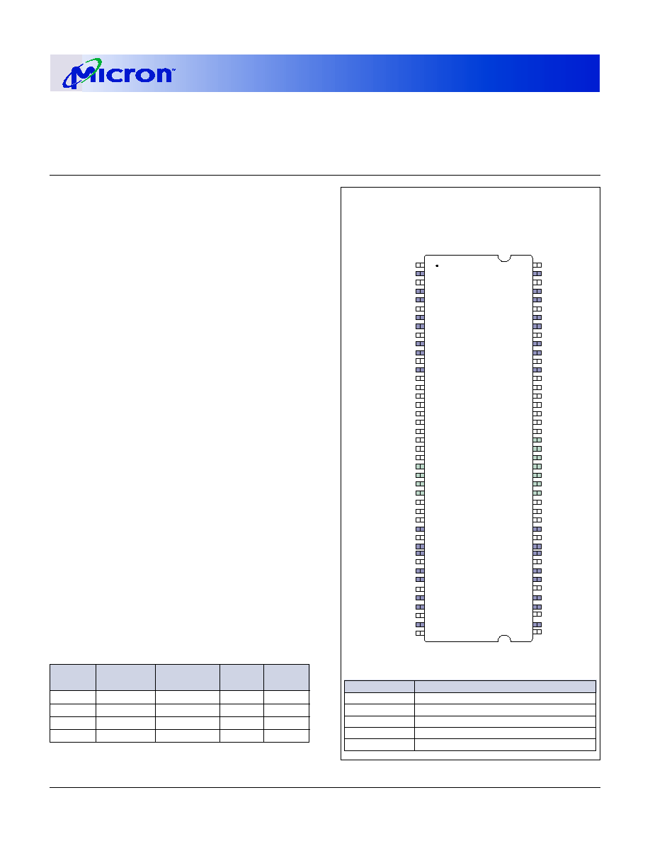
PIN ASSIGNMENT (TOP VIEW)
86-PIN TSOP
FEATURES
∑ PC100 functionality
∑ Fully synchronous; all signals registered on
positive edge of system clock
∑ Internal pipelined operation; column address can
be changed every clock cycle
∑ Internal banks for hiding row access/precharge
∑ Programmable burst lengths: 1, 2, 4, 8, or full page
∑ Auto Precharge, includes CONCURRENT AUTO
PRECHARGE, and Auto Refresh Modes
∑ Self Refresh Mode
∑ 64ms, 4,096-cycle refresh (15.6µs/row)
∑ LVTTL-compatible inputs and outputs
∑ Single +3.3V ±0.3V power supply
∑ Supports CAS latency of 1, 2, and 3
OPTIONS
MARKING
∑ Configuration
2 Meg x 32 (512K x 32 x 4 banks)
2M32B2
∑ Plastic Package - OCPL
1
86-pin TSOP (400 mil)
TG
∑ Timing (Cycle Time)
5ns (200 MHz)
-5
5.5ns (183 MHz)
-55
6ns (166 MHz)
-6
7ns (143 MHz)
-7
∑ Operating Temperature Range
Commercial (0∞ to +70∞C)
None
Extended (-40∞C to +85∞C)
IT
2
NOTE: 1. Off-center parting line
2. Available on -7
Part Number Example:
MT48LC2M32B2TG-7
Note: The # symbol indicates signal is active LOW.
V
DD
DQ
0
V
DD
Q
DQ1
DQ2
V
SS
Q
DQ3
DQ4
V
DD
Q
DQ5
DQ6
V
SS
Q
DQ7
NC
V
DD
DQM0
WE#
CAS#
RAS#
CS#
NC
BA0
BA1
A10
A0
A1
A2
DQM2
V
DD
NC
DQ16
V
SS
Q
DQ17
DQ18
V
DD
Q
DQ19
DQ20
V
SS
Q
DQ21
DQ22
V
DD
Q
DQ23
V
DD
1
2
3
4
5
6
7
8
9
10
11
12
13
14
15
16
17
18
19
20
21
22
23
24
25
26
27
28
29
30
31
32
33
34
35
36
37
38
39
40
41
42
43
86
85
84
83
82
81
80
79
78
77
76
75
74
73
72
71
70
69
68
67
66
65
64
63
62
61
60
59
58
57
56
55
54
53
52
51
50
49
48
47
46
45
44
V
SS
DQ15
V
SS
Q
DQ14
DQ13
V
DD
Q
DQ12
DQ11
V
SS
Q
DQ10
DQ9
V
DD
Q
DQ8
NC
V
SS
DQM1
NC
NC
CLK
CKE
A9
A8
A7
A6
A5
A4
A3
DQM3
V
SS
NC
DQ31
V
DD
Q
DQ30
DQ29
V
SS
Q
DQ28
DQ27
V
DD
Q
DQ26
DQ25
V
SS
Q
DQ24
V
SS
SYNCHRONOUS
DRAM
MT48LC2M32B2 - 512K x 32 x 4 banks
For the latest data sheet, please refer to the Micron Web
site:
www.micron.com/sdramds
KEY TIMING PARAMETERS
SPEED
CLOCK
ACCESS TIME
SETUP
HOLD
GRADE
FREQUENCY
CL = 3*
TIME
TIME
-5
200 MHz
4.5ns
1.5ns
1ns
-55
183 MHz
5ns
1.5ns
1ns
-6
166 MHz
5.5ns
1.5ns
1ns
-7
143 MHz
5.5ns
2ns
1ns
*CL = CAS (READ) latency

2
64Mb: x32 SDRAM
Micron Technology, Inc., reserves the right to change products or specifications without notice.
64MSDRAMx32_5.p65 ≠ Rev. B; Pub. 6/02
©2002, Micron Technology, Inc.
64Mb: x32
SDRAM
The SDRAM provides for programmable READ or
WRITE burst lengths of 1, 2, 4, or 8 locations, or the full
page, with a burst terminate option. An auto precharge
function may be enabled to provide a self-timed row
precharge that is initiated at the end of the burst se-
quence.
The 64Mb SDRAM uses an internal pipelined archi-
tecture to achieve high-speed operation. This archi-
tecture is compatible with the 2n rule of prefetch archi-
tectures, but it also allows the column address to be
changed on every clock cycle to achieve a high-speed,
fully random access. Precharging one bank while ac-
cessing one of the other three banks will hide the
precharge cycles and provide seamless, high-speed,
random-access operation.
The 64Mb SDRAM is designed to operate in 3.3V,
low-power memory systems. An auto refresh mode is
provided, along with a power-saving, power-down
mode. All inputs and outputs are LVTTL-compatible.
SDRAMs offer substantial advances in DRAM oper-
ating performance, including the ability to synchro-
nously burst data at a high data rate with automatic
column-address generation, the ability to interleave
between internal banks to hide precharge time and
the capability to randomly change column addresses
on each clock cycle during a burst access.
GENERAL DESCRIPTION
The 64Mb SDRAM is a high-speed CMOS, dynamic
random-access memory containing 67,108,864-bits. It
is internally configured as a quad-bank DRAM with a
synchronous interface (all signals are registered on the
positive edge of the clock signal, CLK). Each of the
16,777,216-bit banks is organized as 2,048 rows by 256
columns by 32 bits.
Read and write accesses to the SDRAM are burst
oriented; accesses start at a selected location and con-
tinue for a programmed number of locations in a pro-
grammed sequence. Accesses begin with the registra-
tion of an ACTIVE command, which is then followed by
a READ or WRITE command. The address bits regis-
tered coincident with the ACTIVE command are used
to select the bank and row to be accessed (BA0, BA1
select the bank, A0-A10 select the row). The address
bits registered coincident with the READ or WRITE com-
mand are used to select the starting column location
for the burst access.
64Mb (x32) SDRAM PART NUMBER
PART NUMBER
ARCHITECTURE
MT48LC2M32B2TG
2 Meg x 32

3
64Mb: x32 SDRAM
Micron Technology, Inc., reserves the right to change products or specifications without notice.
64MSDRAMx32_5.p65 ≠ Rev. B; Pub. 6/02
©2002, Micron Technology, Inc.
64Mb: x32
SDRAM
TABLE OF CONTENTS
Functional Block Diagram - 2 Meg x 32 .................
4
Pin Descriptions .....................................................
5
Functional Description .........................................
6
Initialization ......................................................
6
Register Definition ............................................
6
Mode Register ...............................................
6
Burst Length ............................................
6
Burst Type ...............................................
7
CAS Latency ............................................
8
Operating Mode ......................................
8
Write Burst Mode ....................................
8
Commands ............................................................
9
Truth Table 1 (Commands and DQM Operation)
............
9
Command Inhibit ............................................. 10
No Operation (NOP) .......................................... 10
Load Mode Register ........................................... 10
Active ................................................................ 10
Read
................................................................ 10
Write ................................................................ 10
Precharge ........................................................... 10
Auto Precharge .................................................. 10
Burst Terminate ................................................. 11
Auto Refresh ...................................................... 11
Self Refresh ........................................................ 11
Operation ............................................................... 12
Bank/Row Activation ........................................ 12
Reads ................................................................ 13
Writes ................................................................ 19
Precharge ........................................................... 21
Power-Down ...................................................... 21
Clock Suspend .................................................. 22
Burst Read/Single Write .................................... 22
Concurrent Auto Precharge .............................. 23
Write with Auto Precharge ............................... 24
Truth Table 2 (CKE)
................................................ 25
Truth Table 3 (Current State, Same Bank)
..................... 26
Truth Table 4 (Current State, Different Bank)
................. 28
Absolute Maximum Ratings .................................. 30
DC Electrical Characteristics
and Operating Conditions ...................................... 30
I
DD
Specifications and Conditions ......................... 30
Capacitance ............................................................ 32
AC Electrical Characteristics (Timing Table) .... 32
AC Electrical Characteristics ................................... 34
Timing Waveforms
Initialize and Load Mode Register .................... 36
Power-Down Mode .......................................... 37
Clock Suspend Mode ........................................ 38
Auto Refresh Mode ........................................... 39
Self Refresh Mode ............................................. 40
Reads
Read ≠ Single Read ....................................... 41
Read ≠ Without Auto Precharge ................. 42
Read ≠ With Auto Precharge ....................... 43
Alternating Bank Read Accesses .................. 44
Read ≠ Full-Page Burst ................................. 45
Read ≠ DQM Operation .............................. 46
Writes
Write ≠ Single Write ..................................... 47
Write ≠ Without Auto Precharge ................ 48
Write ≠ With Auto Precharge ...................... 49
Alternating Bank Write Accesses ................. 50
Write ≠ Full-Page Burst ................................ 51
Write ≠ DQM Operation ............................. 52

4
64Mb: x32 SDRAM
Micron Technology, Inc., reserves the right to change products or specifications without notice.
64MSDRAMx32_5.p65 ≠ Rev. B; Pub. 6/02
©2002, Micron Technology, Inc.
64Mb: x32
SDRAM
FUNCTIONAL BLOCK DIAGRAM
2 Meg x 32 SDRAM
11
RAS#
CAS#
CLK
CS#
WE#
CKE
8
A0-A10,
BA0, BA1
DQM0-
DQM3
13
256
(x32)
8192
I/O GATING
DQM MASK LOGIC
READ DATA LATCH
WRITE DRIVERS
COLUMN
DECODER
BANK0
MEMORY
ARRAY
(2,048 x 256 x 32)
BANK0
ROW-
ADDRESS
LATCH
&
DECODER
2048
SENSE AMPLIFIERS
BANK
CONTROL
LOGIC
DQ0-
DQ31
32
32
DATA
INPUT
REGISTER
DATA
OUTPUT
REGISTER
32
BANK1
BANK0
BANK2
BANK3
11
8
2
4
4
2
REFRESH
COUNTER
11
11
MODE REGISTER
CONTROL
LOGIC
COMMAND
DECODE
ROW-
ADDRESS
MUX
ADDRESS
REGISTER
COLUMN-
ADDRESS
COUNTER/
LATCH
5
64Mb: x32 SDRAM
Micron Technology, Inc., reserves the right to change products or specifications without notice.
64MSDRAMx32_5.p65 ≠ Rev. B; Pub. 6/02
©2002, Micron Technology, Inc.
64Mb: x32
SDRAM
PIN DESCRIPTIONS
PIN NUMBERS
SYMBOL
TYPE
DESCRIPTION
68
CLK
Input
Clock: CLK is driven by the system clock. All SDRAM input signals are
sampled on the positive edge of CLK. CLK also increments the internal burst
counter and controls the output registers.
67
CKE
Input
Clock Enable: CKE activates (HIGH) and deactivates (LOW) the CLK signal.
Deactivating the clock provides PRECHARGE POWER-DOWN and SELF REFRESH
operation (all banks idle), ACTIVE POWER-DOWN (row active in any bank) or
CLOCK SUSPEND operation (burst/access in progress). CKE is synchronous
except after the device enters power-down and self refresh modes, where
CKE becomes asynchronous until after exiting the same mode. The input
buffers, including CLK, are disabled during power-down and self refresh
modes, providing low standby power. CKE may be tied HIGH.
20
CS#
Input
Chip Select: CS# enables (registered LOW) and disables (registered HIGH) the
command decoder. All commands are masked when CS# is registered HIGH.
CS# provides for external bank selection on systems with multiple banks.
CS# is considered part of the command code.
17, 18, 19
WE#, CAS#,
Input
Command Inputs: WE# , CAS#, and RAS# (along with CS#) define the
RAS#
command being entered.
16, 71, 28, 59
DQM0-
Input
Input/Output Mask: DQM is sampled HIGH and is an input mask signal
DQM3
for write accesses and an output enable signal for read accesses. Input data
is masked during a WRITE cycle. The output buffers are placed in a High-Z
state (two-clock latency) during a READ cycle. DQM0 corresponds to DQ0-
DQ7; DQM1 corresponds to DQ8-DQ15; DQM2 corresponds to DQ16-DQ23;
and DQM3 corresponds to DQ24-DQ31. DQM0-DQM3 are considered same
state when referenced as DQM.
22, 23
BA0, BA1
Input
Bank Address Input(s): BA0 and BA1 define to which bank the ACTIVE, READ,
WRITE or PRECHARGE command is being applied.
25-27, 60-66, 24
A0-A10
Input
Address Inputs: A0-A10 are sampled during the ACTIVE command (row-
address A0-A10) and READ/WRITE command (column-address A0-A7 with A10
defining auto precharge) to select one location out of the memory array in
the respective bank. A10 is sampled during a PRECHARGE command to
determine if all banks are to be precharged (A10 HIGH) or bank selected by
BA0, BA1 (LOW). The address inputs also provide the op-code during a LOAD
MODE REGISTER command.
2, 4, 5, 7, 8, 10, 11, 13,
DQ0-DQ31
Input/
Data I/Os: Data bus.
74, 76, 77, 79, 80, 82, 83,
Output
85, 31, 33, 34, 36, 37, 39,
40, 42, 45, 47, 48, 50, 51,
53, 54, 56
14, 21, 30, 57, 69, 70, 73
NC
≠
No Connect: These pins should be left unconnected. Pin 70 is reserved
for SSTL reference voltage supply.
3, 9, 35, 41, 49, 55, 75, 81
V
DD
Q
Supply
DQ Power Supply: Isolated on the die for improved noise immunity.
6, 12, 32, 38, 46, 52, 78, 84
V
SS
Q
Supply
DQ Ground: Provide isolated ground to DQs for improved noise immunity.
1, 15, 29, 43
V
DD
Supply
Power Supply: +3.3V ±0.3V. (See note 27 on page 35.)
44, 58, 72, 86
V
SS
Supply
Ground.