Document Outline
- Features/Options
- 16Mb (x4/x8) SDRAM Part Numbers
- Key Timing Parameters
- 44-Pin TSOP Pin Assignment
- General Description
- Table of Contents
- Functional Block Diagram, 4 Meg x 4 SDRAM
- Functional Block Diagram, 2 Meg x 8 SDRAM
- Pin Descriptions
- Functional Description
- Initialization
- Register Definition
- Mode Register
- Burst Length
- Burst Type
- Figure 1, Mode Register Definition
- Table 1, Burst Definition
- CAS Latency
- Operating Mode
- Write Burst Mode
- Figure 2, CAS LATENCY
- Table 2, CAS LATENCY
- Commands
- Truth Table 1 - Commands and DQM Operation
- Command Inhibit
- NO OPERATION (NOP)
- LOAD MODE REGISTER
- ACTIVE
- READ
- WRITE
- PRECHARGE
- Auto Precharge
- BURST TERMINATE
- AUTO REFRESH
- SELF REFRESH
- Operation
- Bank/Row Activation
- Figure 3, Activating a Specific Row in a Specific Bank
- Example: Meeting tRCD (MIN) When 2 < tRCD (MIN)/tCK < 3
- READs
- Figure 5, READ Command
- Figure 6, CAS Latency
- Figure 7, Consecutive READ Bursts
- Figure 8, Random READ Accesses
- Figure 9, READ to WRITE
- Figure 10, READ to WRITE with Extra Clock Cycle
- Figure 11, READ to PRECHARGE
- Figure 12, Terminating a READ Burst
- WRITEs
- Figure 13, WRITE Command
- Figure 14, WRITE Burst
- Figure 15, WRITE to WRITE
- Figure 16, RANDOM WRITE Cycles
- Figure 17, WRITE to READ
- Figure 18, WRITE to PRECHARGE
- Figure 19, Terminating a WRITE Burst
- Figure 20, PRECHARGE Command
- PRECHARGE
- Power-Down
- Figure 21, Power-Down
- Clock Suspend Mode
- Figure 22, CLOCK SUSPEND During WRITE Burst
- Burst Read/Single Write
- Figure 23, CLOCK SUSPEND During READ Burst
- CONCURRENT AUTO PRECHARGE
- Figure 24, READ with Auto Precharge Interrupted by a READ
- Figure 25, READ with Auto Precharge Interrupted by a WRITE
- Figure 26, WRITE with Auto Precharge Interrupted by a READ
- Figure 27, WRITE with Auto Precharge Interrupted by a WRITE
- Truth Table 2 - CKE
- Truth Table 3 - Current State Bank n - Command to Bank n
- Truth Table 4 - Current State Bank n - Command to Bank m
- Absolute Maximum Ratings
- DC Electrical Characteristics and Operating Conditions
- Icc Specifications and Conditions
- Capacitance
- Electrical Characteristics and Recommended AC Operating Conditions
- AC Functional Characteristics
- Electrical Timing Characteristics Between -8 Speed Options
- Notes
- Timing Diagrams
- Initialize and Load Mode Register
- Power-Down Mode
- Clock Suspend Mode
- Auto Refresh Mode
- Self Refresh Mode
- READ Ö Without AutoPrecharge
- READ Ö With AutoPrecharge
- Alternating Bank READ Accesses
- READ Ö Full-Page Burst
- READ Ö DQM Operation
- WRITE Ö Without AutoPrecharge
- WRITE Ö With AutoPrecharge
- Alternating Bank WRITE Accesses
- WRITE Ö Full-Page Burst
- WRITE Ö DQM Operation
- 44-Pin Plastic TSOP (400 mil) Package Drawing
PRODUCTS AND SPECIFICATIONS DISCUSSED HEREIN ARE SUBJECT TO CHANGE BY MICRON WITHOUT NOTICE.
1
16 Meg: x4, x8 SDRAM
©1998, Micron Technology, Inc.
16MSDRAMx4x8_B.p65 ≠ Rev. 5/98
16 MEG: x4, x8
SDRAM
16Mb (x4/x8) SDRAM PART NUMBERS
PART NUMBER
ARCHITECTURE
MT48LC4M4A1TG S
4 Meg x 4 (
t
WR = 1 CLK)
MT48LC2M8A1TG S
2 Meg x 8 (
t
WR = 1 CLK)
4 MEG x 4
2 MEG x 8
Configuration
2 Meg x 4 x 2 banks 1 Meg x 8 x 2 banks
Refresh Count
4K
4K
Row Addressing
2K (A0-A10)
2K (A0-A10)
Bank Addressing
2 (BA)
1 (BA)
Column Addressing
1K (A0-A9)
512 (A0-A8)
FEATURES
∑ PC100-compliant; includes CONCURRENT AUTO
PRECHARGE
∑ Fully synchronous; all signals registered on positive
edge of system clock
∑ Internal pipelined operation; column address can be
changed every clock cycle
∑ Internal banks for hiding row access/precharge
∑ Programmable burst lengths: 1, 2, 4, 8, or full page
∑ Auto Precharge and Auto Refresh Modes
∑ Self Refresh Mode
∑ 64ms, 4,096-cycle refresh
∑ LVTTL-compatible inputs and outputs
∑ Single +3.3V ±0.3V power supply
∑ Longer lead TSOP for improved reliability (OCPL*)
∑ One- and two-clock WRITE recovery (
t
WR) versions
OPTIONS
MARKING
∑ Configurations
4 Meg x 4 (2 Meg x 4 x 2 banks)
4M4
2 Meg x 8 (1 Meg x 8 x 2 banks)
2M8
∑ WRITE Recovery (
t
WR/
t
DPL)
t
WR = 1 CLK
A1
t
WR = 2 CLK (Contact factory for availability.)A2
∑ Plastic Package - OCPL*
44-pin TSOP (400 mil)
TG
∑ Timing (Cycle Time)
8ns;
t
AC = 6ns @ CL = 3
-8B
10ns;
t
AC = 9ns @ CL = 2
-10
NOTE: The 16Mb SDRAM base number differentiates the
offerings in two places: MT48LC2M8A1 S. The fourth
field distinguishes the architecture offering: 4M4
designates 4 Meg x 4, and 2M8 designates 2 Meg x 8.
The fifth field distinguishes the WRITE recovery
offering: A1 designates one CLK and A2 designates two
CLKs.
Part Number Example:
MT48LC2M8A1TG-10 S
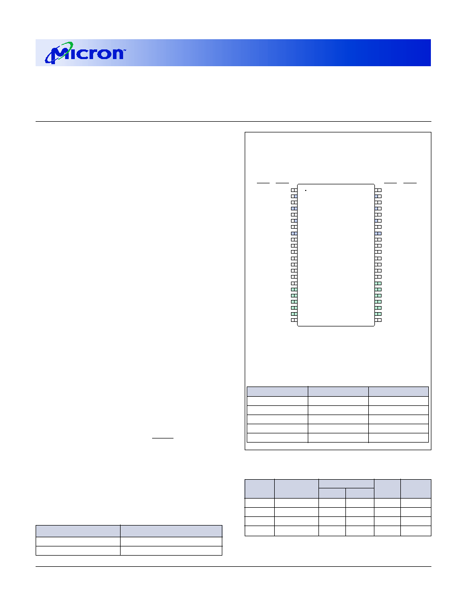
PIN ASSIGNMENT (Top View)
44-Pin TSOP
V
DD
DQ0
VssQ
DQ1
V
DD
Q
DQ2
VssQ
DQ3
V
DD
Q
NC
NC
WE#
CAS#
RAS#
CS#
BA
A10
A0
A1
A2
A3
V
DD
1
2
3
4
5
6
7
8
9
10
11
12
13
14
15
16
17
18
19
20
21
22
44
43
42
41
40
39
38
37
36
35
34
33
32
31
30
29
28
27
26
25
24
23
Vss
DQ7
VssQ
DQ6
V
DD
Q
DQ5
VssQ
DQ4
V
DD
Q
NC
NC
DQM
CLK
CKE
NC
A9
A8
A7
A6
A5
A4
Vss
-
NC
-
DQ0
-
NC
-
DQ1
-
-
-
-
-
-
-
-
-
-
-
-
-
-
-
NC
-
DQ3
-
NC
-
DQ2
-
-
-
-
-
-
-
-
-
-
-
-
-
-
x4
x8
x8
x4
NOTE: The # symbol indicates signal is active LOW. A dash
(-) indicates x4 pin function is same as x8 pin
function.
SYNCHRONOUS
DRAM
MT48LC4M4A1/A2 S - 2 Meg x 4 x 2 banks
MT48LC2M8A1/A2 S - 1 Meg x 8 x 2 banks
For the latest data sheet revisions, please refer to the
Micron Web site:
www.micron.com/datasheets
.
KEY TIMING PARAMETERS
SPEED
CLOCK
ACCESS TIME
SETUP
HOLD
GRADE
FREQUENCY CL = 2** CL = 3**
TIME
TIME
-8B
125 MHz
≠
6ns
2ns
1ns
-10
100 MHz
≠
7.5ns
3ns
1ns
-8B
83 MHz
9ns
≠
2ns
1ns
-10
66 MHz
9ns
≠
3ns
1ns
* Off-center parting line
**CL = CAS (READ) latency

2
16 Meg: x4, x8 SDRAM
Micron Technology, Inc., reserves the right to change products or specifications without notice.
16MSDRAMx4x8_B.p65 ≠ Rev. 5/98
©1998, Micron Technology, Inc.
16 MEG: x4, x8
SDRAM
GENERAL DESCRIPTION
The Micron 16Mb SDRAM is a high-speed CMOS,
dynamic random-access memory containing 16,777,216
bits. It is internally configured as a dual memory array
(the 4 Meg x 4 is a dual 2 Meg x 4, and the 2 Meg x 8 is a dual
1 Meg x 8) with a synchronous interface (all signals are
registered on the positive edge of the clock signal, CLK).
Each of the two internal banks is organized with 2,048
rows and either 1,024 columns by 4 bits (4 Meg x 4) or 512
columns by 8 bits (2 Meg x 8).
Read and write accesses to the SDRAM are burst ori-
ented; accesses start at a selected location and continue
for a programmed number of locations in a programmed
sequence. Accesses begin with the registration of an AC-
TIVE command, which is then followed by a READ or
WRITE command. The address bits registered coinci-
dent with the ACTIVE command are used to select the
bank and row to be accessed (BA selects the bank, A0-A10
select the row). The address bits registered coincident
with the READ or WRITE command are used to select the
starting column location for the burst access.
The SDRAM provides for programmable READ or
WRITE burst lengths of 1, 2, 4, or 8 locations, or the full
page, with a burst terminate option. An auto precharge
function may be enabled to provide a self-timed row
precharge that is initiated at the end of the burst
sequence.
The Micron 16Mb SDRAM uses an internal pipelined
architecture to achieve high-speed operation. This ar-
chitecture is compatible with the 2n rule of prefetch
architectures, but it also allows the column address to be
changed on every clock cycle to achieve a high-speed,
fully random access. Precharging one bank while access-
ing the alternate bank will hide the PRECHARGE cycles
and provide seamless, high-speed, random-access op-
eration.
The Micron 16Mb SDRAM is designed to operate in
3.3V, low-power memory systems. An auto refresh mode
is provided, along with a power-saving, power-down
mode. All inputs and outputs are LVTTL-compatible.
SDRAMs offer substantial advances in DRAM operat-
ing performance, including the ability to synchronously
burst data at a high data rate with automatic column-
address generation, the ability to interleave between in-
ternal banks in order to hide precharge time, and the
capability to randomly change column addresses on each
clock cycle during a burst access.

3
16 Meg: x4, x8 SDRAM
Micron Technology, Inc., reserves the right to change products or specifications without notice.
16MSDRAMx4x8_B.p65 ≠ Rev. 5/98
©1998, Micron Technology, Inc.
16 MEG: x4, x8
SDRAM
TABLE OF CONTENTS
Functional Block Diagram - 4 Meg x 4 ........................
4
Functional Block Diagram - 2 Meg x 8 ........................
5
Pin Descriptions ............................................................
6
Functional Description ................................................
7
Initialization .............................................................
7
Register Definitions .................................................
7
Mode Register .....................................................
7
Burst Length ..................................................
7
Burst Type .....................................................
7
CAS Latency ..................................................
9
Operating Mode ............................................
9
Write Burst Mode .........................................
9
Commands ..................................................................... 10
Truth Table 1 (Commands and DQM Operation)
....... 10
Command Inhibit .............................................. 11
No Operation (NOP) .......................................... 11
Load Mode Register ........................................... 11
Active ................................................................... 11
Read ..................................................................... 11
Write .................................................................... 11
Precharge ............................................................ 11
Auto Precharge ................................................... 11
Burst Terminate ................................................. 11
Auto Refresh ....................................................... 12
Self Refresh ......................................................... 12
Operation ....................................................................... 13
Bank/Row Activation ......................................... 13
Reads ................................................................... 14
Writes .................................................................. 20
Precharge ............................................................ 22
Power-Down ....................................................... 22
Clock Suspend .................................................... 23
Burst Read/Single Write .................................... 23
Concurrent Auto Precharge .............................. 24
Truth Table 2 (CKE)
................................................. 26
Truth Table 3 (Current State)
.................................... 27
Truth Table 4 (Current State)
.................................... 29
Absolute Maximum Ratings ......................................... 31
DC Electrical Characteristics and Operating Conditions . 31
I
CC
Operating Conditions and Maximum Limits ........ 31
Capacitance .................................................................... 32
AC Electrical Characteristics (Timing Table) ............ 32
Timing Waveforms
Initialize and Load Mode Register ......................... 35
Power-Down Mode .................................................. 36
Clock Suspend Mode ............................................... 37
Auto Refresh Mode .................................................. 38
Self Refresh Mode .................................................... 39
Reads
Read - Without Auto Precharge ........................ 40
Read - With Auto Precharge .............................. 41
Alternating Bank Read Accesses ....................... 42
Read - Full-Page Burst ....................................... 43
Read - DQM Operation ...................................... 44
Writes
Write - Without Auto Precharge ....................... 45
Write - With Auto Precharge ............................. 46
Alternating Bank Write Accesses ...................... 47
Write - Full-Page Burst ...................................... 48
Write - DQM Operation ..................................... 49

4
16 Meg: x4, x8 SDRAM
Micron Technology, Inc., reserves the right to change products or specifications without notice.
16MSDRAMx4x8_B.p65 ≠ Rev. 5/98
©1998, Micron Technology, Inc.
16 MEG: x4, x8
SDRAM
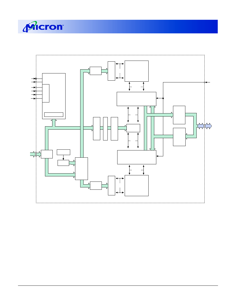
FUNCTIONAL BLOCK DIAGRAM
4 Meg x 4 SDRAM
11
11
11
RAS#
REFRESH
CONTROLLER
2,048
REFRESH
COUNTER
CAS#
1,024
1,024 (x4)
10
COLUMN-
ADDRESS BUFFER
BURST COUNTER
ROW-
ADDRESS
MUX
CLK
CS#
WE#
CKE
1,024 (x4)
BANK 1
MEMORY
ARRAY
(2,048 x 1,024 x 4)
SENSE AMPLIFIERS
I/O GATING
DQM MASK LOGIC
CONTROL
LOGIC
COLUMN
DECODER
COLUMN-
ADDRESS LATCH
10
MODE REGISTER
ROW-
ADDRESS
LATCH
11
ROW
DECODER
11
COMMAND
DECODE
DQ0 -
DQ3
A0-A10, BA
4
8
DQM
1,024
2,048
BANK 0
MEMORY
ARRAY
(2,048 x 1,024 x 4)
ROW
DECODER
ROW-
ADDRESS
LATCH
11
12
ADDRESS
REGISTER
12
SENSE AMPLIFIERS
I/O GATING
DQM MASK LOGIC
DATA
INPUT
REGISTER
DATA
OUTPUT
REGISTER
4
4
5
16 Meg: x4, x8 SDRAM
Micron Technology, Inc., reserves the right to change products or specifications without notice.
16MSDRAMx4x8_B.p65 ≠ Rev. 5/98
©1998, Micron Technology, Inc.
16 MEG: x4, x8
SDRAM
FUNCTIONAL BLOCK DIAGRAM
2 Meg x 8 SDRAM
11
11
11
RAS#
REFRESH
CONTROLLER
2,048
REFRESH
COUNTER
CAS#
512
512 (x8)
9
COLUMN-
ADDRESS BUFFER
BURST COUNTER
ROW-
ADDRESS
MUX
CLK
CS#
WE#
CKE
512 (x8)
BANK 1
MEMORY
ARRAY
(2,048 x 512 x 8)
SENSE AMPLIFIERS
I/O GATING
DQM MASK LOGIC
CONTROL
LOGIC
COLUMN
DECODER
COLUMN-
ADDRESS LATCH
9
MODE REGISTER
ROW-
ADDRESS
LATCH
11
ROW
DECODER
11
COMMAND
DECODE
DQ0 -
DQ7
A0-A10, BA
8
8
DQM
512
2,048
BANK 0
MEMORY
ARRAY
(2,048 x 512 x 8)
ROW
DECODER
ROW-
ADDRESS
LATCH
11
12
ADDRESS
REGISTER
12
SENSE AMPLIFIERS
I/O GATING
DQM MASK LOGIC
DATA
INPUT
REGISTER
DATA
OUTPUT
REGISTER
8
8