1
128Mb: x16, x32 Mobile SDRAM
Micron Technology, Inc., reserves the right to change products or specifications without notice.
MobileY95W_3V_F.p65 � Rev. F; Pub. 9/02
�2002, Micron Technology, Inc.
128Mb: x16, x32
MOBILE SDRAM
ADVANCE
PRODUCTS AND SPECIFICATIONS DISCUSSED HEREIN ARE FOR EVALUATION AND REFERENCE PUROPOSES ONLY AND ARE SUBJECT TO CHANGE BY
MICRON WITHOUT NOTICE. PRODUCTS ARE ONLY WARRANTED BY MICRON TO MEET MICRON'S PRODUCTION AND DATA SHEET SPECIFICATIONS.
8 Meg x 16
4 Meg x 32
Configuration
2 Meg x 16 x 4 banks 1 Meg x 32 x 4 banks
Refresh Count
4K
4K
Row Addressing
4K (A0�A11)
4K (A0�A11)
Bank Addressing
4 (BA0, BA1)
4 (BA0, BA1)
Column Addressing
512 (A0�A8)
256 (A0�A7)
SYNCHRONOUS
DRAM
MT48LC8M16LFFF, MT48V8M16LFFF � 2 Meg x 16 x 4 banks
MT48LC4M32LFFC , MT48V4M32LFFC � 1 Meg x 32 x 4 banks
For the latest data sheet revisions, please refer to the Micron Web
site:
www.micron.com/dramds
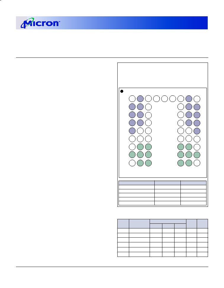
PIN ASSIGNMENT (Top View)
54-Ball VFBGA
FEATURES
� Temperature Compensated Self Refresh (TCSR)
� Fully synchronous; all signals registered on positive
edge of system clock
� Internal pipelined operation; column address can be
changed every clock cycle
� Internal banks for hiding row access/precharge
� Programmable burst lengths: 1, 2, 4, 8, or full page
� Auto Precharge, includes CONCURRENT AUTO
PRECHARGE, and Auto Refresh Modes
� Self Refresh Mode; standard and low power
� 64ms, 4,096-cycle refresh
� LVTTL-compatible inputs and outputs
� Low voltage power supply
� Partial Array Self Refresh power-saving mode
� Operating Temperature Range
Industrial (-40
o
C to +85
o
C)
OPTIONS
MARKING
� V
DD
/V
DD
Q
3.3V/3.3V
LC
2.5V/2.5V or 1.8V
V
� Configurations
8 Meg x 16 (2 Meg x 16 x 4 banks)
8M16
4 Meg x 32 (1 Meg x 32 x 4 banks)
4M32
� Package/Ball out
Plastic Package
54-ball FBGA (8mm x 9mm)(x16 only)
FF
1
90-ball FBGA (11mm x 13mm)
FC
1
� Timing (Cycle Time)
8ns @ CL = 3 (125 MHz)
-8
10ns @ CL = 3 (100 MHz)
-10
Part Number Example:
MT48V8M16LFFC-8
NOTE: 1. See page 61 for FBGA/VFBGA Device Marking
Table.
KEY TIMING PARAMETERS
SPEED
CLOCK
ACCESS TIME
t
RCD
t
RP
GRADE FREQUENCY CL=1* CL=2* CL=3*
-8
125 MHz
�
�
7ns
20ns
20ns
-10
100 MHz
�
�
7ns
20ns
20ns
-8
100 MHz
�
8ns
�
20ns
20ns
-10
83 MHz
�
8ns
�
20ns
20ns
-8
50 MHz
19ns
�
�
20ns
20ns
-10
40 MHz
22ns
�
�
20ns
20ns
*CL = CAS (READ) latency
A
B
C
D
E
F
G
H
J
1 2 3 4 5 6 7 8
Top View
(Ball Down)
V
SS
DQ14
DQ12
DQ10
DQ8
UDQM
NC/A12
A8
V
SS
DQ15
DQ13
DQ11
DQ9
NC
CLK
A11
A7
A5
V
SS
Q
V
DD
Q
V
SS
Q
V
DD
Q
V
SS
CKE
A9
A6
A4
V
DD
Q
V
SS
Q
V
DD
Q
V
SS
Q
V
DD
CAS#
BA0
A0
A3
DQ0
DQ2
DQ4
DQ6
LDQM
RAS#
BA1
A1
A2
V
DD
DQ1
DQ3
DQ5
DQ7
WE#
CS#
A10
V
DD
9
2
128Mb: x16, x32 Mobile SDRAM
Micron Technology, Inc., reserves the right to change products or specifications without notice.
MobileY95W_3V_F.p65 � Rev. F; Pub. 9/02
�2002, Micron Technology, Inc.
128Mb: x16, x32
MOBILE SDRAM
ADVANCE
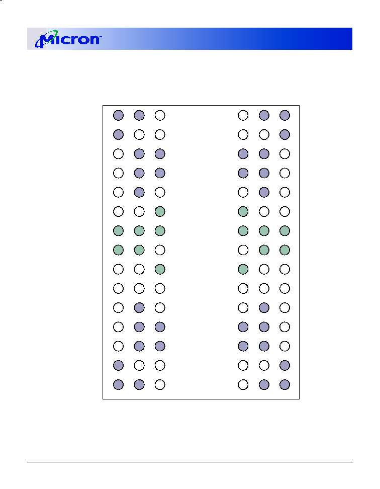
90-Ball FBGA PIN ASSIGNMENT
(Top View)
1
2
3
4
6
7
8
9
5
DQ26
DQ28
V
SS
Q
V
SS
Q
V
DD
Q
V
SS
A4
A7
CLK
DQM1
V
DD
Q
V
SS
Q
V
SS
Q
DQ11
DQ13
DQ24
V
DD
Q
DQ27
DQ29
DQ31
DQM3
A5
A8
CKE
NC
DQ8
DQ10
DQ12
V
DD
Q
DQ15
V
SS
V
SS
Q
DQ25
DQ30
NC
A3
A6
NC
A9
NC
V
SS
DQ9
DQ14
V
SS
Q
V
SS
V
DD
V
DD
Q
DQ22
DQ17
NC
A2
A10
NC
BA0
CAS#
V
DD
DQ6
DQ1
V
DD
Q
V
DD
DQ21
DQ19
V
DD
Q
V
DD
Q
V
SS
Q
V
DD
A1
A11
RAS#
DQM0
V
SS
Q
V
DD
Q
V
DD
Q
DQ4
DQ2
DQ23
V
SS
Q
DQ20
DQ18
DQ16
DQM2
A0
BA1
CS#
WE#
DQ7
DQ5
DQ3
V
SS
Q
DQ0
A
B
C
D
E
F
G
H
J
K
L
M
N
P
R
Ball and Array
3
128Mb: x16, x32 Mobile SDRAM
Micron Technology, Inc., reserves the right to change products or specifications without notice.
MobileY95W_3V_F.p65 � Rev. F; Pub. 9/02
�2002, Micron Technology, Inc.
128Mb: x16, x32
MOBILE SDRAM
ADVANCE
precharge that is initiated at the end of the burst se-
quence.
The 128Mb SDRAM uses an internal pipelined
architecture to achieve high-speed operation. This
architecture is compatible with the 2n rule of prefetch
architectures, but it also allows the column address to be
changed on every clock cycle to achieve a high-speed,
fully random access. Precharging one bank while access-
ing one of the other three banks will hide the precharge
cycles and provide seamless high-speed, random-access
operation.
The 128Mb SDRAM is designed to operate in 3.3V or
2.5V, low-power memory systems. An auto refresh mode
is provided, along with a power-saving, power-down
mode. All inputs and outputs are LVTTL-compatible.
SDRAMs offer substantial advances in DRAM operat-
ing performance, including the ability to synchronously
burst data at a high data rate with automatic column-
address generation, the ability to interleave between in-
ternal banks in order to hide precharge time and the
capability to randomly change column addresses on each
clock cycle during a burst access.
GENERAL DESCRIPTION
The Micron
�
128Mb SDRAM is a high-speed CMOS,
dynamic random-access memory containing 134,217,728
bits. It is internally configured as a quad-bank DRAM
with a synchronous interface (all signals are registered on
the positive edge of the clock signal, CLK). Each of the
x16's 33,554,432-bit banks is organized as 4,096 rows by
512 columns by 16 bits. Each of the x32's 33,554,432-bit
banks is organized as 4,096 rows by 256 columns by 32
bits.
Read and write accesses to the SDRAM are burst ori-
ented; accesses start at a selected location and continue
for a programmed number of locations in a programmed
sequence. Accesses begin with the registration of an AC-
TIVE command, which is then followed by a READ or
WRITE command. The address bits registered coinci-
dent with the ACTIVE command are used to select the
bank and row to be accessed (BA0, BA1 select the bank;
A0-A11 select the row). The address bits registered coin-
cident with the READ or WRITE command are used to
select the starting column location for the burst access.
The SDRAM provides for programmable READ or
WRITE burst lengths of 1, 2, 4, or 8 locations, or the full
page, with a burst terminate option. An auto precharge
function may be enabled to provide a self-timed row
PART NUMBER
V
DD
/V
DD
Q
ARCHITECTURE
PACKAGE
MT48LC8M16LFFF-xx
3.3V / 3.3V
8 Meg x 16
54-BALL VFBGA
MT48V8M16LFFF-xx
2.5V / 2.5V-1.8V
8 Meg x 16
54-BALL VFBGA
MT48LC4M32LFFC-xx
3.3V / 3.3V
4 Meg x 32
90-BALL FBGA
MT48V4M32LFFC-xx
2.5V / 2.5V-1.8V
4 Meg x 32
90-BALL FBGA
128Mb SDRAM PART NUMBERS

4
128Mb: x16, x32 Mobile SDRAM
Micron Technology, Inc., reserves the right to change products or specifications without notice.
MobileY95W_3V_F.p65 � Rev. F; Pub. 9/02
�2002, Micron Technology, Inc.
128Mb: x16, x32
MOBILE SDRAM
ADVANCE
TABLE OF CONTENTS
Functional Block Diagram � 8 Meg x 16 ................
5
Functional Block Diagram � 4 Meg x 32 ................
6
54-Ball Pin Descriptions .........................................
7
90-Ball Pin Descriptions .........................................
8
Functional Description .........................................
9
Initialization ......................................................
9
Register Definition ............................................
9
mode register ................................................
9
Burst Length ............................................
9
Burst Type ............................................... 10
CAS Latency ............................................ 11
Operating Mode ...................................... 11
Extended Mode Register ......................... 12
Temperature Compensated Self Refresh . 12
Partial Array Self Refresh ......................... 13
Commands ............................................................. 14
Truth Table 1 (Commands and DQM Operation)
............ 14
Command Inhibit ............................................. 15
No Operation (NOP) .......................................... 15
Load mode register ............................................ 15
Active ................................................................ 15
Read
................................................................ 15
Write ................................................................ 15
Precharge ........................................................... 15
Auto Precharge .................................................. 15
Burst Terminate ................................................. 15
Auto Refresh ...................................................... 16
Self Refresh ........................................................ 16
Operation ................................................................ 17
Bank/Row Activation ........................................ 17
Reads ................................................................ 18
Writes ................................................................ 24
Precharge ........................................................... 26
Concurrent Auto Precharge .............................. 28
Truth Table 2 (CKE)
................................................ 30
Truth Table 3 (Current State, Same Bank)
..................... 31
Truth Table 4 (Current State, Different Bank)
................. 33
Absolute Maximum Ratings ................................... 35
DC Electrical Characteristics
and Operating Conditions ................................... 35
AC Electrical Characteristics and Recommended
Operating Conditions (Timing Table) ............. 36
AC Functional Characteristics ................................ 37
I
DD
Specifications and Conditions ......................... 37
Capacitance ............................................................ 38
Timing Waveforms
Initialize and Load mode register ...................... 40
Power-Down Mode ............................................ 41
Clock Suspend Mode ......................................... 42
Auto Refresh Mode ............................................ 43
Self Refresh Mode .............................................. 44
Reads
Read � Without Auto Precharge ................... 45
Read � With Auto Precharge ........................ 46
Single Read � Without Auto Precharge ........ 47
Single Read � With Auto Precharge ............. 48
Alternating Bank Read Accesses ................... 49
Read � Full-Page Burst .................................. 50
Read � DQM Operation ................................ 51
Writes
Write � Without Auto Precharge ................. 52
Write � With Auto Precharge ....................... 53
Single Write � Without Auto Precharge ....... 54
Single Write � With Auto Precharge ............ 55
Alternating Bank Write Accesses ................. 56
Write � Full-Page Burst ................................. 57
Write � DQM Operation .............................. 58
54-Ball VFBGA Drawing ............................... 59
90-Ball FBGA Drawing ................................. 60
FBGA/VFBGA Device Marking ..................... 61
Power-Down ...................................................... 26
Clock Suspend ................................................... 27
Burst Read/Single Write .................................... 27
5
128Mb: x16, x32 Mobile SDRAM
Micron Technology, Inc., reserves the right to change products or specifications without notice.
MobileY95W_3V_F.p65 � Rev. F; Pub. 9/02
�2002, Micron Technology, Inc.
128Mb: x16, x32
MOBILE SDRAM
ADVANCE
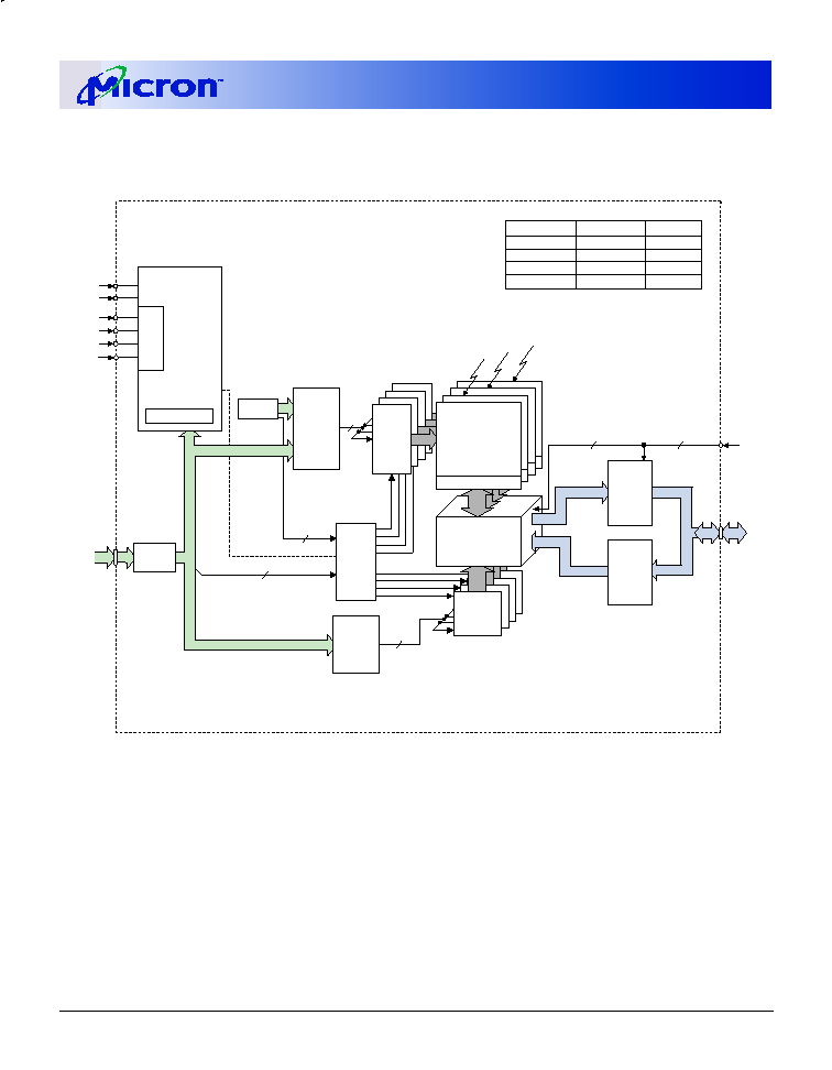
FUNCTIONAL BLOCK DIAGRAM
8 Meg x16 SDRAM
12
RAS#
CAS#
ROW-
ADDRESS
MUX
CLK
CS#
WE#
CKE
CONTROL
LOGIC
COLUMN-
ADDRESS
COUNTER/
LATCH
MODE REGISTER
9
COMMAND
DECODE
A0-A11,
BA0, BA1
DQML,
DQMH
12
ADDRESS
REGISTER
14
512
(x16)
4096
I/O GATING
DQM MASK LOGIC
READ DATA LATCH
WRITE DRIVERS
COLUMN
DECODER
BANK0
MEMORY
ARRAY
(4,096 x 512 x 16)
BANK0
ROW-
ADDRESS
LATCH
&
DECODER
4096
SENSE AMPLIFIERS
BANK
CONTROL
LOGIC
DQ0-
DQ15
16
16
DATA
INPUT
REGISTER
DATA
OUTPUT
REGISTER
16
12
BANK1
BANK2
BANK3
12
9
2
2
2
2
REFRESH
COUNTER
BA1
BA0
Bank
0
0
0
0
1
1
1
0
2
1
1
3

6
128Mb: x16, x32 Mobile SDRAM
Micron Technology, Inc., reserves the right to change products or specifications without notice.
MobileY95W_3V_F.p65 � Rev. F; Pub. 9/02
�2002, Micron Technology, Inc.
128Mb: x16, x32
MOBILE SDRAM
ADVANCE
FUNCTIONAL BLOCK DIAGRAM
4 Meg x 32 SDRAM
12
RAS#
CAS#
CLK
CS#
WE#
CKE
8
A0�A11,
BA0, BA1
DQM0�
DQM3
14
256
(x32)
8192
I/O GATING
DQM MASK LOGIC
READ DATA LATCH
WRITE DRIVERS
COLUMN
DECODER
BANK0
MEMORY
ARRAY
(4,096 x 256 x 32)
BANK0
ROW-
ADDRESS
LATCH
&
DECODER
4096
SENSE AMPLIFIERS
BANK
CONTROL
LOGIC
DQ0�
DQ31
32
32
DATA
INPUT
REGISTER
DATA
OUTPUT
REGISTER
32
BANK1
BANK0
BANK2
BANK3
12
8
2
4
4
2
REFRESH
COUNTER
12
12
MODE REGISTER
CONTROL
LOGIC
COMMAND
DECODE
ROW-
ADDRESS
MUX
ADDRESS
REGISTER
COLUMN-
ADDRESS
COUNTER/
LATCH
BA1
BA0
Bank
0
0
1
1
0
1
0
1
0
1
2
3

7
128Mb: x16, x32 Mobile SDRAM
Micron Technology, Inc., reserves the right to change products or specifications without notice.
MobileY95W_3V_F.p65 � Rev. F; Pub. 9/02
�2002, Micron Technology, Inc.
128Mb: x16, x32
MOBILE SDRAM
ADVANCE
BALL DESCRIPTIONS
54-BALL VFBGA
SYMBOL
TYPE
DESCRIPTION
F2
CLK
Input
Clock: CLK is driven by the system clock. All SDRAM input signals are sampled
on the positive edge of CLK. CLK also increments the internal burst counter
and controls the output registers.
F3
CKE
Input
Clock Enable: CKE activates (HIGH) and deactivates (LOW) the CLK signal.
Deactivating the clock provides PRECHARGE POWER-DOWN and SELF REFRESH
operation (all banks idle), ACTIVE POWER-DOWN (row active in any bank) or
CLOCK SUSPEND operation (burst/access in progress). CKE is synchronous
except after the device enters power-down and self refresh modes, where
CKE becomes asynchronous until after exiting the same mode. The input
buffers, including CLK, are disabled during power-down and self refresh
modes, providing low standby power. CKE may be tied HIGH.
G9
CS#
Input
Chip Select: CS# enables (registered LOW) and disables (registered HIGH) the
command decoder. All commands are masked when CS# is registered HIGH.
CS# provides for external bank selection on systems with multiple banks. CS#
is considered part of the command code.
F7, F8, F9
CAS#, RAS#,
Input
Command Inputs: CAS#, RAS#, and WE# (along with CS#) define the
WE#
command being entered.
E8, F1
LDQM,
Input
Input/Output Mask: DQM is sampled HIGH and is an input mask signal for
UDQM
write accesses and an output enable signal for read accesses. Input data is
masked during a WRITE cycle. The output buffers are placed in a High-Z state
(two-clock latency) when during a READ cycle. LDQM corresponds to DQ0�
DQ7, UDQM corresponds to DQ8�DQ15. LDQM and UDQM are considered
same state when referenced as DQM.
G7, G8
BA0, BA1
Input
Bank Address Input(s): BA0 and BA1 define to which bank the ACTIVE, READ,
WRITE or PRECHARGE command is being applied. These pins also provide the
op-code during a LOAD MODE REGISTER command
H7, H8, J8, J7, J3, J2,
A0�A11
Input
Address Inputs: A0�A11 are sampled during the ACTIVE command (row-
H3, H2, H1, G3, H9, G2,
address A0�A11) and READ/WRITE command (column-address A0�A8; with
A10 defining auto precharge) to select one location out of the memory array
in the respective bank. A10 is sampled during a PRECHARGE command to
determine if all banks are to be precharged (A10 HIGH) or bank selected by
BA0, BA1 (LOW). The address inputs also provide the op-code during a LOAD
MODE REGISTER command.
A8, B9, B8, C9, C8, D9,
DQ0�DQ15
I/O
Data Input/Output: Data bus
D8, E9, E1, D2, D1, C2,
C1, B2, B1, A2
E2, G1
NC
�
No Connect: These pins should be left unconnected.
G1 is a no connect for this part but may be used as A12 in future designs.
A7, B3, C7, D3
V
DD
Q
Supply
DQ Power: Isolated power on the die to improve noise immunity.
A3, B7, C3, D7,
V
SS
Q
Supply
DQ Ground: Isolated power on the die to improve noise immunity.
A9, E7, J9
V
DD
Supply
Power Supply: Voltage dependant on option.
A1, E3, J1
V
SS
Supply
Ground.
8
128Mb: x16, x32 Mobile SDRAM
Micron Technology, Inc., reserves the right to change products or specifications without notice.
MobileY95W_3V_F.p65 � Rev. F; Pub. 9/02
�2002, Micron Technology, Inc.
128Mb: x16, x32
MOBILE SDRAM
ADVANCE
BALL DESCRIPTIONS
90-BALL FBGA
SYMBOL
TYPE
DESCRIPTION
J1
CLK
Input
Clock: CLK is driven by the system clock. All SDRAM input signals are sampled
on the positive edge of CLK. CLK also increments the internal burst counter
and controls the output registers.
J2
CKE
Input
Clock Enable: CKE activates (HIGH) and deactivates (LOW) the CLK signal.
Deactivating the clock provides PRECHARGE POWER-DOWN and SELF REFRESH
operation (all banks idle), ACTIVE POWER-DOWN (row active in any bank) or
CLOCK SUSPEND operation (burst/access in progress). CKE is synchronous
except after the device enters power-down and self refresh modes, where
CKE becomes asynchronous until after exiting the same mode. The input
buffers, including CLK, are disabled during power-down and self refresh
modes, providing low standby power. CKE may be tied HIGH.
J8
CS#
Input
Chip Select: CS# enables (registered LOW) and disables (registered HIGH) the
command decoder. All commands are masked when CS# is registered HIGH.
CS# provides for external bank selection on systems with multiple banks. CS#
is considered part of the command code.
J9, K7, K8
RAS#, CAS#
Input
Command Inputs: RAS#, CAS#, and WE# (along with CS#) define the
WE#
command being entered.
K9, K1, F8, F2
DQM0�3
Input
Input/Output Mask: DQM is sampled HIGH and is an input mask signal for
write accesses and an output enable signal for read accesses. Input data is
masked during a WRITE cycle. The output buffers are placed in a High-Z state
(two-clock latency) when during a READ cycle. DQM0 corresponds to DQ0�
DQ7, DQM1 corresponds to DQ8�DQ15, DQM2 corresponds to DQ16�DQ23
and DQM3 corresponds to DQ24�DQ31. DQM0-3 are considered same state
when referenced as DQM.
J7, H8
BA0, BA1
Input
Bank Address Input(s): BA0 and BA1 define to which bank the ACTIVE, READ,
WRITE or PRECHARGE command is being applied. These pins also provide the
op-code during a LOAD MODE REGISTER command
G8, G9, F7, F3, G1, G2,
A0�A11
Input
Address Inputs: A0�A11 are sampled during the ACTIVE command (row-
G3, H1, H2, J3, G7, H9
address A0�A11) and READ/WRITE command (column-address A0�A7; with
A10 defining auto precharge) to select one location out of the memory array
in the respective bank. A10 is sampled during a PRECHARGE command to
determine if all banks are to be precharged (A10 HIGH) or bank selected by
BA0, BA1 (LOW). The address inputs also provide the op-code during a LOAD
MODE REGISTER command.
R8, N7, R9, N8, P9, M8,
DQ0�DQ31
I/O
Data Input/Output: Data bus
M7, L8, L2, M3, M2, P1, N2,
R1, N3, R2, E8, D7, D8, B9,
C8, A9, C7, A8, A2, C3, A1,
C2, B1, D2, D3, E2
E3, E7, H3, H7, K2, K3
NC
�
No Connect: These pins should be left unconnected.
H7 and H9 are not connects for this part but may be used as A12 and A11 in
future designs.
B2, B7, C9, D9, E1,
V
DD
Q
Supply
DQ Power: Isolated power on the die to improve noise immunity.
L1, M9, N9, P2, P7
B8, B3, C1, D1, E9,
V
SS
Q
Supply
DQ Ground: Isolated power on the die to improve noise immunity.
L9, M1, N1, P3, P8
A7, F9, L7, R7
V
DD
Supply
Power Supply: Voltage dependant on option.
A3, F1, L3, R3
V
SS
Supply
Ground.

9
128Mb: x16, x32 Mobile SDRAM
Micron Technology, Inc., reserves the right to change products or specifications without notice.
MobileY95W_3V_F.p65 � Rev. F; Pub. 9/02
�2002, Micron Technology, Inc.
128Mb: x16, x32
MOBILE SDRAM
ADVANCE
FUNCTIONAL DESCRIPTION
In general, the 128Mb SDRAMs (2 Meg x16 x 4 banks
and 1 Meg x 32 x 4 banks) are quad-bank DRAMs that
operate at 3.3V or 2.5V and include a synchronous inter-
face (all signals are registered on the positive edge of the
clock signal, CLK). Each of the x16's 33,554,432-bit banks
is organized as 4,096 rows by 512 columns by 16 bits.
Each of the x32's 33,554,432-bit banks is organized as
4,096 rows by 256 columns by 32bits.
Read and write accesses to the SDRAM are burst ori-
ented; accesses start at a selected location and continue
for a programmed number of locations in a programmed
sequence. Accesses begin with the registration of an AC-
TIVE command, which is then followed by a READ or
WRITE command. The address bits registered coincident
with the ACTIVE command are used to select the bank
and row to be accessed (BA0 and BA1 select the bank, A0-
A11 select the row). The address bits ( x16: A0-A8; x32: A0-
A7; ) registered coincident with the READ or WRITE com-
mand are used to select the starting column location for
the burst access.
Prior to normal operation, the SDRAM must be initial-
ized. The following sections provide detailed informa-
tion covering device initialization, register definition,
command descriptions and device operation.
Initialization
SDRAMs must be powered up and initialized in a
predefined manner. Operational procedures other than
those specified may result in undefined operation. Once
power is applied to V
DD
and V
DD
Q (simultaneously) and
the clock is stable (stable clock is defined as a signal
cycling within timing constraints specified for the clock
pin), the SDRAM requires a 100�s delay prior to issuing
any command other than a COMMAND INHIBIT or NOP.
Starting at some point during this 100�s period and con-
tinuing at least through the end of this period, COM-
MAND INHIBIT or NOP commands should be applied.
Once the 100�s delay has been satisfied with at least
one COMMAND INHIBIT or NOP command having been
applied, a PRECHARGE command should be applied. All
banks must then be precharged, thereby placing the
device in the all banks idle state.
Once in the idle state, two AUTO REFRESH cycles
must be performed. After the AUTO REFRESH cycles are
complete, the SDRAM is ready for mode register pro-
gramming. Because the mode register will power up in an
unknown state, it should be loaded prior to applying any
operational command.
Register Definition
MODE REGISTER
In order to achieve low power consumption, there are
two mode registers in the Mobile component, Mode Reg-
ister and Extended Mode Register. For this section, Mode
Register is referred to. Extended Mode register is dis-
cussed on page 12. The mode register is used to define the
specific mode of operation of the SDRAM. This definition
includes the selection of a burst length, a burst type, a
CAS latency, an operating mode and a write burst mode,
as shown in Figure 1. The mode register is programmed
via the LOAD MODE REGISTER command and will retain
the stored information until it is programmed again or
the device loses power.
Mode Register bits M0-M2 specify the burst length,
M3 specifies the type of burst (sequential or interleaved),
M4-M6 specify the CAS latency, M7 and M8 specify the
operating mode, M9, M10, and M11 should be set to zero.
M12 and M13 should be set to zero to prevent extended
mode register.
The mode register must be loaded when all banks are
idle, and the controller must wait the specified time
before initiating the subsequent operation. Violating ei-
ther of these requirements will result in unspecified op-
eration.
Burst Length
Read and write accesses to the SDRAM are burst ori-
ented, with the burst length being programmable, as
shown in Figure 1. The burst length determines the maxi-
mum number of column locations that can be accessed
for a given READ or WRITE command. Burst lengths of 1,
2, 4, or 8 locations are available for both the sequential
and the interleaved burst types, and a full-page burst is
available for the sequential type. The full-page burst is
used in conjunction with the BURST TERMINATE com-
mand to generate arbitrary burst lengths.
Reserved states should not be used, as unknown op-
eration or incompatibility with future versions may re-
sult.
When a READ or WRITE command is issued, a block of
columns equal to the burst length is effectively selected.
All accesses for that burst take place within this block,
meaning that the burst will wrap within the block if a
boundary is reached. The block is uniquely selected by
A1-A8 (x16) or A1-A7 (x32) when the burst length is set to
two; by A2-A8 (x16) or A2-A7 (x32) when the burst length
is set to four; and by A3-A8 (x16) or A3-A7 (x32) when the
burst length is set to eight. The remaining (least signifi-
cant) address bit(s) is (are) used to select the starting
location within the block. Full-page bursts wrap within
the page if the boundary is reached.
10
128Mb: x16, x32 Mobile SDRAM
Micron Technology, Inc., reserves the right to change products or specifications without notice.
MobileY95W_3V_F.p65 � Rev. F; Pub. 9/02
�2002, Micron Technology, Inc.
128Mb: x16, x32
MOBILE SDRAM
ADVANCE
NOTE: 1. For full-page accesses: y = 512 (x16), y = 256
(x32).
2. For a burst length of two, A1-A8 (x16) or A1-A7
(x32) select the block-of-two burst; A0 selects
the starting column within the block.
3. For a burst length of four, A2-A8 (x16) or A2-A7
(x32) select the block-of-four burst; A0-A1 select
the starting column within the block.
4. For a burst length of eight, A3-A8 (x16) or A3-
A7 (x32) select the block-of-eight burst; A0-A2
select the starting column within the block.
5. For a full-page burst, the full row is selected
and A0-A8 (x16) or A0-A7 (x32) select the
starting column.
6. Whenever a boundary of the block is reached
within a given sequence above, the following
access wraps within the block.
7. For a burst length of one, A0-A8 (x16) or A0-A7
(x32) select the unique column to be accessed,
and mode register bit M3 is ignored.
Table 1
Burst Definition
Burst
Starting Column
Order of Accesses Within a Burst
Length
Address
Type = Sequential Type = Interleaved
A0
2
0
0-1
0-1
1
1-0
1-0
A1 A0
0
0
0-1-2-3
0-1-2-3
4
0
1
1-2-3-0
1-0-3-2
1
0
2-3-0-1
2-3-0-1
1
1
3-0-1-2
3-2-1-0
A2 A1 A0
0
0
0
0-1-2-3-4-5-6-7
0-1-2-3-4-5-6-7
0
0
1
1-2-3-4-5-6-7-0
1-0-3-2-5-4-7-6
0
1
0
2-3-4-5-6-7-0-1
2-3-0-1-6-7-4-5
8
0
1
1
3-4-5-6-7-0-1-2
3-2-1-0-7-6-5-4
1
0
0
4-5-6-7-0-1-2-3
4-5-6-7-0-1-2-3
1
0
1
5-6-7-0-1-2-3-4
5-4-7-6-1-0-3-2
1
1
0
6-7-0-1-2-3-4-5
6-7-4-5-2-3-0-1
1
1
1
7-0-1-2-3-4-5-6
7-6-5-4-3-2-1-0
Full
n = A0-A11
Cn, Cn + 1, Cn + 2
Page
Cn + 3, Cn + 4...
Not Supported
(y)
(location 0-y)
...Cn - 1,
Cn...
Figure 1
Mode Register Definition
Burst Type
Accesses within a given burst may be programmed to
be either sequential or interleaved; this is referred to as
the burst type and is selected via bit M3.
The ordering of accesses within a burst is determined
by the burst length, the burst type and the starting col-
umn address, as shown in Table 1.
10
M3 = 0
1
2
4
8
Reserved
Reserved
Reserved
Full Page
M3 = 1
1
2
4
8
Reserved
Reserved
Reserved
Reserved
Operating Mode
Standard Operation
All other states reserved
0
-
0
-
Defined
-
0
1
Burst Type
Sequential
Interleaved
CAS Latency
Reserved
1
2
3
Reserved
Reserved
Reserved
Reserved
Burst Length
M0
0
1
0
1
0
1
0
1
Burst Length
CAS Latency
BT
A9
A7
A6
A5
A4
A3
A8
A2
A1
A0
Mode Register (Mx)
Address Bus
9
7
6
5
4
3
8
2
1
0
M1
0
0
1
1
0
0
1
1
M2
0
0
0
0
1
1
1
1
M3
M4
0
1
0
1
0
1
0
1
M5
0
0
1
1
0
0
1
1
M6
0
0
0
0
1
1
1
1
M6-M0
M8
M7
Op Mode
A10
Reserved* WB
0
1
Write Burst Mode
Programmed Burst Length
Single Location Access
M9
*Should program
M10 = "0, 0"
to ensure compatibility
with future devices.
BA0
BA1
M9
M7 M6
M5
M4
M3
M8
M2
M1
M0
M10
11
A11
M11
M12
M13
Reserved**
13
12
** BA1, BA0 = "0, 0"
to prevent Extended
Mode Register.
11
128Mb: x16, x32 Mobile SDRAM
Micron Technology, Inc., reserves the right to change products or specifications without notice.
MobileY95W_3V_F.p65 � Rev. F; Pub. 9/02
�2002, Micron Technology, Inc.
128Mb: x16, x32
MOBILE SDRAM
ADVANCE
ALLOWABLE OPERATING
FREQUENCY (MHz)
CAS
CAS
CAS
SPEED
LATENCY = 1
LATENCY = 2
LATENCY = 3
- 8
50
100
125
- 10
40
83
100
Operating Mode
The normal operating mode is selected by setting M7
and M8 to zero; the other combinations of values for M7
and M8 are reserved for future use and/or test modes.
The programmed burst length applies to both READ and
WRITE bursts.
Test modes and reserved states should not be used
because unknown operation or incompatibility with fu-
ture versions may result.
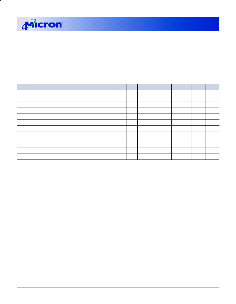
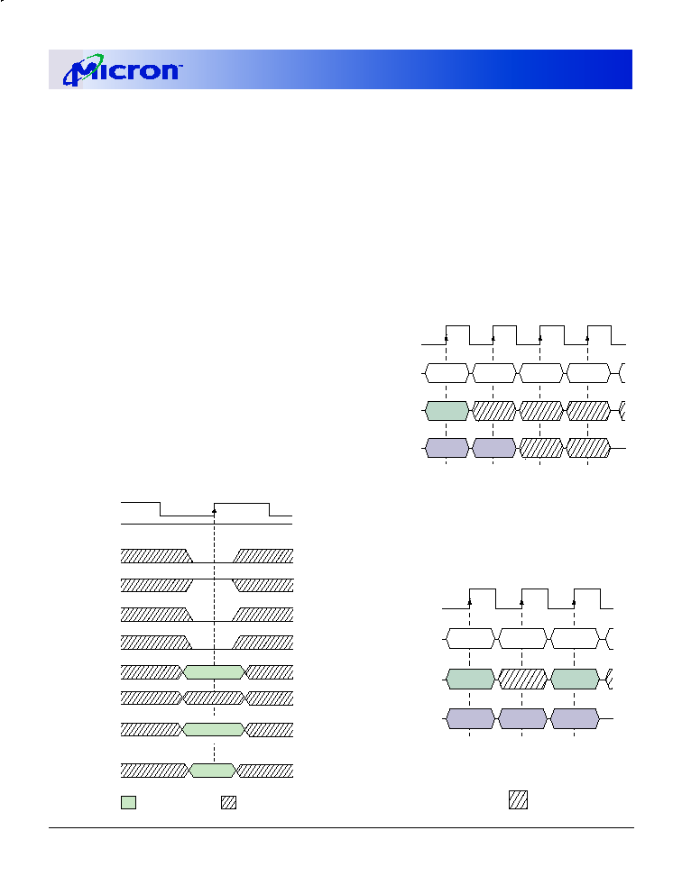
CAS Latency
The CAS latency is the delay, in clock cycles, between
the registration of a READ command and the availability
of the first piece of output data. The latency can be set to
one, two, or three clocks.
If a READ command is registered at clock edge n, and
the latency is m clocks, the data will be available by clock
edge n + m. The DQs will start driving as a result of the
clock edge one cycle earlier (n + m - 1), and provided that
the relevant access times are met, the data will be valid by
clock edge n + m. For example, assuming that the clock
cycle time is such that all relevant access times are met,
if a READ command is registered at T0 and the latency is
programmed to two clocks, the DQs will start driving
after T1 and the data will be valid by T2, as shown in
Figure 2. Table 2 indicates the operating frequencies at
which each CAS latency setting can be used.
Reserved states should not be used as unknown op-
eration or incompatibility with future versions
may result.
Figure 2
CAS Latency
Table 2
CAS Latency
CLK
DQ
T2
T1
T3
T0
CAS Latency = 3
LZ
D
OUT
tOH
t
COMMAND
NOP
READ
tAC
NOP
T4
NOP
DON'T CARE
UNDEFINED
CLK
DQ
T2
T1
T0
CAS Latency = 1
LZ
D
OUT
tOH
t
COMMAND
NOP
READ
tAC
CLK
DQ
T2
T1
T3
T0
CAS Latency = 2
LZ
D
OUT
tOH
t
COMMAND
NOP
READ
tAC
NOP
12
128Mb: x16, x32 Mobile SDRAM
Micron Technology, Inc., reserves the right to change products or specifications without notice.
MobileY95W_3V_F.p65 � Rev. F; Pub. 9/02
�2002, Micron Technology, Inc.
128Mb: x16, x32
MOBILE SDRAM
ADVANCE
EXTENDED MODE REGISTER
The Extended Mode Register controls the functions
beyond those controlled by the Mode Register. These
additional functions are special features of the Mobile
device. They include Temperature Compensated Self Re-
fresh (TCSR) Control, and Partial Array Self Refresh
(PASR).
The Extended Mode Register is programmed via the
Mode Register Set command (BA1=1,BA0=0) and retains
the stored information until it is programmed again or
the device loses power.
The Extended Mode Register must be programmed
with M5 through M11 set to "0". The Extended Mode
Register must be loaded when all banks are idle and no
bursts are in progress, and the controller must wait the
specified time before before initiating any subsequent
operation. Violating either of these requirements results
in unspecified operation.
TEMPERATURE COMPENSATED SELF REFRESH
Temperature Compensated Self Refresh (TCSR) al-
lows the controller to program the Refresh interval dur-
ing SELF REFRESH mode, according to the case tempera-
ture of the Mobile device. This allows great power savings
during SELF REFRESH during most operating tempera-
ture ranges. Only during extreme temperatures would
the controller have to select a TCSR level that will guaran-
tee data during SELF REFRESH.
Every cell in the DRAM requires refreshing due to the
capacitor losing its charge over time. The refresh rate is
dependent on temperature. At higher temperatures a
capacitor loses charge quicker than at lower tempera-
tures, requiring the cells to be refreshed more often.
Historically, during Self Refresh, the refresh rate has
been set to accomodate the worst case, or highest tem-
perature range expected.
EXTENDED MODE REGISTER TABLE
Maximum Case Temp
A4 A3
A9
A7 A6 A5 A4 A3
A8
A2 A1 A0
Extended Mode
Register (Ex)
Address Bus
9
7
6
5
4
3
8
2
1
0
A10
A11
10
11
12
PASR
TCSR
0
13
1
All must be set to "0"
BA0
M9
M7 M6 M5 M4 M3
M8
M2 M1 M0
M10
M11
M12
BA1
M13
85�C
1
1
70�C
0
0
45�C
15�C
0
1
1
0
Notes: 1. E13 and E12 (BA1 and BA0) must be "1, 0" to select the
Extended Mode Register (vs. the base Mode Register).
2. RFU: Reserved for Future Use
Self Refresh Coverage
Four Banks
Two Banks (Bank 0,1)
One Bank (Bank 0)
RFU
RFU
RFU
RFU
RFU
A2
A1
A0
0
0
0
0
0
0
0
0
0
0
1
1
1
1
1
1
1
1
0
0
1
1
1
1

13
128Mb: x16, x32 Mobile SDRAM
Micron Technology, Inc., reserves the right to change products or specifications without notice.
MobileY95W_3V_F.p65 � Rev. F; Pub. 9/02
�2002, Micron Technology, Inc.
128Mb: x16, x32
MOBILE SDRAM
ADVANCE
Thus, during ambient temperatures, the power
consumed during refresh was unnecessarily high,
because the refresh rate was set to accommodate the
higher temperatures. Setting M4 and M3, allow the
DRAM to accomodate more specific temperature
regions during SELF REFRESH. There are four
temperature settings, which will vary the SELF
REFRESH current according to the selected tempera-
ture. This selectable refresh rate will save power when
the DRAM is operating at normal temperatures.
PARTIAL ARRAY SELF REFRESH
For further power savings during SELF REFRESH, the
Partial Array Self Refresh (PASR) feature allows the con-
troller to select the amount of memory that will be re-
freshed during SELF REFRESH. The refresh options are
all banks (banks 0, 1, 2, and 3); two banks(banks 0 and 1);
and one bank (bank 0). WRITE and READ commands
occur to any bank selected during standard operation,
but only the selected banks in PASR will be refreshed
during SELF REFRESH. It's important to note that data
in banks 2 and 3 will be lost when the two bank option is
used. Data will be lost in banks 1, 2, and 3 when the one
bank option is used.
14
128Mb: x16, x32 Mobile SDRAM
Micron Technology, Inc., reserves the right to change products or specifications without notice.
MobileY95W_3V_F.p65 � Rev. F; Pub. 9/02
�2002, Micron Technology, Inc.
128Mb: x16, x32
MOBILE SDRAM
ADVANCE
TRUTH TABLE 1 � COMMANDS AND DQM OPERATION
(Note: 1)
NAME (FUNCTION)
CS# RAS# CAS# WE# DQM
ADDR
DQs
NOTES
COMMAND INHIBIT (NOP)
H
X
X
X
X
X
X
NO OPERATION (NOP)
L
H
H
H
X
X
X
ACTIVE (Select bank and activate row)
L
L
H
H
X
Bank/Row
X
3
READ (Select bank and column, and start READ burst)
L
H
L
H
L/H
8
Bank/Col
X
4
WRITE (Select bank and column, and start WRITE burst)
L
H
L
L
L/H
8
Bank/Col
Valid
4
BURST TERMINATE
L
H
H
L
X
X
Active
PRECHARGE (Deactivate row in bank or banks)
L
L
H
L
X
Code
X
5
AUTO REFRESH or SELF REFRESH
L
L
L
H
X
X
X
6, 7
(Enter self refresh mode)
LOAD MODE REGISTER
L
L
L
L
X
Op-Code
X
2
Write Enable/Output Enable
�
�
�
�
L
�
Active
8
Write Inhibit/Output High-Z
�
�
�
�
H
�
High-Z
8
following the Operation section; these tables provide
current state/next state information.
Commands
Truth Table 1 provides a quick reference of available
commands. This is followed by a written description of
each command. Three additional Truth Tables appear
NOTE: 1. CKE is HIGH for all commands shown except SELF REFRESH.
2. A0-A10 define the op-code written to the mode register.
3. A0-A11 provide row address, and BA0, BA1 determine which bank is made active.
4. A0-A8 (x16) or A0-A7 (x32) provide column address; A10 HIGH enables the auto precharge feature (nonpersistent),
while A10 LOW disables the auto precharge feature; BA0, BA1 determine which bank is being read from or written to.
5. A10 LOW: BA0, BA1 determine the bank being precharged. A10 HIGH: All banks precharged and BA0, BA1 are "Don't
Care."
6. This command is AUTO REFRESH if CKE is HIGH, SELF REFRESH if CKE is LOW.
7. Internal refresh counter controls row addressing; all inputs and I/Os are "Don't Care" except for CKE.
8. Activates or deactivates the DQs during WRITEs (zero-clock delay) and READs (two-clock delay). DQM0 controls DQ0-
7, DQM1 controls DQ8-15, DQM2 controls DQ16-23, and DQM3 controls DQ24-31.

15
128Mb: x16, x32 Mobile SDRAM
Micron Technology, Inc., reserves the right to change products or specifications without notice.
MobileY95W_3V_F.p65 � Rev. F; Pub. 9/02
�2002, Micron Technology, Inc.
128Mb: x16, x32
MOBILE SDRAM
ADVANCE
COMMAND INHIBIT
The COMMAND INHIBIT function prevents new com-
mands from being executed by the SDRAM, regardless of
whether the CLK signal is enabled. The SDRAM is effec-
tively deselected. Operations already in progress are not
affected.
NO OPERATION (NOP)
The NO OPERATION (NOP) command is used to per-
form a NOP to an SDRAM which is selected (CS# is LOW).
This prevents unwanted commands from being regis-
tered during idle or wait states. Operations already in
progress are not affected.
LOAD MODE REGISTER
The mode register is loaded via inputs A0, BA0, BA1.
See mode register heading in the Register Definition
section. The LOAD MODE REGISTER and LOAD EX-
TENDED MODE REGISTER commands can only be is-
sued when all banks are idle, and a subsequent execut-
able command cannot be issued until
t
MRD is met.
ACTIVE
The ACTIVE command is used to open (or activate) a
row in a particular bank for a subsequent access. The
value on the BA0, BA1 inputs selects the bank, and the
address provided on inputs A0-A11 selects the row. This
row remains active (or open) for accesses until a
PRECHARGE command is issued to that bank. A
PRECHARGE command must be issued before opening a
different row in the same bank.
READ
The READ command is used to initiate a burst read
access to an active row. The value on the BA0, BA1 inputs
selects the bank, and the address provided on inputs A0-
A8 (x16) or A0-A7 (x32) selects the starting column loca-
tion. The value on input A10 determines whether or not
auto precharge is used. If auto precharge is selected, the
row being accessed will be precharged at the end of the
READ burst; if auto precharge is not selected, the row will
remain open for subsequent accesses. Read data appears
on the DQs subject to the logic level on the DQM inputs
two clocks earlier. If a given DQM signal was registered
HIGH, the corresponding DQs will be High-Z two clocks
later; if the DQM signal was registered LOW, the DQs will
provide valid data.
WRITE
The WRITE command is used to initiate a burst write
access to an active row. The value on the BA0, BA1 inputs
selects the bank, and the address provided on inputs A0-
A8 (x16) or A0-A7 (x32) selects the starting column loca-
tion. The value on input A10 determines whether or not
auto precharge is used. If auto precharge is selected, the
row being accessed will be precharged at the end of the
WRITE burst; if auto precharge is not selected, the row
will remain open for subsequent accesses. Input data
appearing on the DQs is written to the memory array
subject to the DQM input logic level appearing coinci-
dent with the data. If a given DQM signal is registered
LOW, the corresponding data will be written to memory;
if the DQM signal is registered HIGH, the corresponding
data inputs will be ignored, and a WRITE will not be
executed to that byte/column location.
PRECHARGE
The PRECHARGE command is used to deactivate the
open row in a particular bank or the open row in all banks.
The bank(s) will be available for a subsequent row access
a specified time (
t
RP) after the PRECHARGE command is
issued. Input A10 determines whether one or all banks
are to be precharged, and in the case where only one bank
is to be precharged, inputs BA0, BA1 select the bank.
Otherwise BA0, BA1 are treated as "Don't Care." Once a
bank has been precharged, it is in the idle state and must
be activated prior to any READ or WRITE commands
being issued to that bank.
AUTO PRECHARGE
Auto precharge is a feature which performs the same
individual-bank PRECHARGE function described above,
without requiring an explicit command. This is accom-
plished by using A10 to enable auto precharge in con-
junction with a specific READ or WRITE command. A
PRECHARGE of the bank/row that is addressed with the
READ or WRITE command is automatically performed
upon completion of the READ or WRITE burst, except in
the full-page burst mode, where auto precharge does not
apply. Auto precharge is nonpersistent in that it is either
enabled or disabled for each individual READ or WRITE
command.
Auto precharge ensures that the precharge is initiated
at the earliest valid stage within a burst. The user must
not issue another command to the same bank until the
precharge time (
t
RP) is completed. This is determined as
if an explicit PRECHARGE command was issued at the
earliest possible time, as described for each burst type in
the Operation section of this data sheet.
BURST TERMINATE
The BURST TERMINATE command is used to trun-
cate either fixed-length or full-page bursts. The most
recently registered READ or WRITE command prior to
the BURST TERMINATE command will be truncated, as
shown in the Operation section of this data sheet.

16
128Mb: x16, x32 Mobile SDRAM
Micron Technology, Inc., reserves the right to change products or specifications without notice.
MobileY95W_3V_F.p65 � Rev. F; Pub. 9/02
�2002, Micron Technology, Inc.
128Mb: x16, x32
MOBILE SDRAM
ADVANCE
AUTO REFRESH
AUTO REFRESH is used during normal operation of
the SDRAM and is analogous to CAS#-BEFORE-RAS#
(CBR) REFRESH in conventional DRAMs. This
command is nonpersistent, so it must be issued each
time a refresh is required. All active banks must be
PRECHARGED prior to issuing an AUTO REFRESH
command. The AUTO REFRESH command should not
be issued until the minimum
t
RP has been met after the
PRECHARGE command as shown in the operation sec-
tion.
The addressing is generated by the internal refresh
controller. This makes the address bits "Don't Care"
during an AUTO REFRESH command. The 128Mb SDRAM
requires 4,096 AUTO REFRESH cycles every 64ms (
t
REF),
regardless of width option. Providing a distributed AUTO
REFRESH command every 15.625�s will meet the refresh
requirement and ensure that each row is refreshed. Alter-
natively, 4,096 AUTO REFRESH commands can be issued
in a burst at the minimum cycle rate (
t
RFC), once every
64ms.
SELF REFRESH
The SELF REFRESH command can be used to retain
data in the SDRAM, even if the rest of the system is
powered down. When in the self refresh mode, the SDRAM
retains data without external clocking. The SELF RE-
FRESH command is initiated like an AUTO REFRESH
command except CKE is disabled (LOW). Once the SELF
REFRESH command is registered, all the inputs to the
SDRAM become "Don't Care" with the exception of CKE,
which must remain LOW.
Once self refresh mode is engaged, the SDRAM pro-
vides its own internal clocking, causing it to perform its
own AUTO REFRESH cycles. The SDRAM must remain in
self refresh mode for a minimum period equal to
t
RAS
and may remain in self refresh mode for an indefinite
period beyond that.
The procedure for exiting self refresh requires a se-
quence of commands. First, CLK must be stable (stable
clock is defined as a signal cycling within timing con-
straints specified for the clock pin) prior to CKE going
back HIGH. Once CKE is HIGH, the SDRAM must have
NOP commands issued (a minimum of two clocks) for
t
XSR because time is required for the completion of any
internal refresh in progress.
Upon exiting the self refresh mode, AUTO REFRESH
commands must be issued every 15.625�s or less as both
SELF REFRESH and AUTO REFRESH utilize the row re-
fresh counter.
17
128Mb: x16, x32 Mobile SDRAM
Micron Technology, Inc., reserves the right to change products or specifications without notice.
MobileY95W_3V_F.p65 � Rev. F; Pub. 9/02
�2002, Micron Technology, Inc.
128Mb: x16, x32
MOBILE SDRAM
ADVANCE
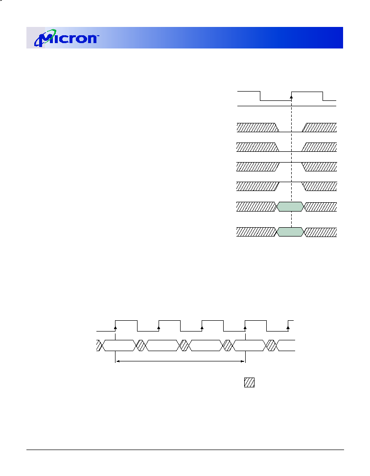
Operation
BANK/ROW ACTIVATION
Before any READ or WRITE commands can be issued
to a bank within the SDRAM, a row in that bank must be
"opened." This is accomplished via the ACTIVE com-
mand, which selects both the bank and the row to be
activated (see Figure 3).
After opening a row (issuing an ACTIVE command), a
READ or WRITE command may be issued to that row,
subject to the
t
RCD specification.
t
RCD (MIN) should be
divided by the clock period and rounded up to the next
whole number to determine the earliest clock edge after
the ACTIVE command on which a READ or WRITE com-
mand can be entered. For example, a
t
RCD specification
of 20ns with a 125 MHz clock (8ns period) results in 2.5
clocks, rounded to 3. This is reflected in Figure 4, which
covers any case where 2 <
t
RCD (MIN)/
t
CK
3. (The same
procedure is used to convert other specification limits
from time units to clock cycles.)
A subsequent ACTIVE command to a different row in
the same bank can only be issued after the previous
active row has been "closed" (precharged). The mini-
mum time interval between successive ACTIVE com-
mands to the same bank is defined by
t
RC.
A subsequent ACTIVE command to another bank can
be issued while the first bank is being accessed, which
results in a reduction of total row-access overhead. The
minimum time interval between successive ACTIVE com-
mands to different banks is defined by
t
RRD.
Figure 4
Example: Meeting
t
RCD (MIN) When 2 <
t
RCD (MIN)/
t
CK
3
CLK
T2
T1
T3
T0
t
COMMAND
NOP
ACTIVE
READ or
WRITE
T4
NOP
RCD
DON'T CARE
CS#
WE#
CAS#
RAS#
CKE
CLK
A0�A10, A11
ROW
ADDRESS
HIGH
BA0, BA1
BANK
ADDRESS
Figure 3
Activating a Specific Row in a
Specific Bank
18
128Mb: x16, x32 Mobile SDRAM
Micron Technology, Inc., reserves the right to change products or specifications without notice.
MobileY95W_3V_F.p65 � Rev. F; Pub. 9/02
�2002, Micron Technology, Inc.
128Mb: x16, x32
MOBILE SDRAM
ADVANCE
Upon completion of a burst, assuming no other com-
mands have been initiated, the DQs will go High-Z. A full-
page burst will continue until terminated. (At the end of
the page, it will wrap to column 0 and continue.)
Data from any READ burst may be truncated with a
subsequent READ command, and data from a fixed-length
READ burst may be immediately followed by data from a
READ command. In either case, a continuous flow of data
can be maintained. The first data element from the new
burst follows either the last element of a completed burst
or the last desired data element of a longer burst that is
being truncated. The new READ command should be
issued x cycles before the clock edge at which the last
desired data element is valid, where x equals the CAS
latency minus one.
READs
READ bursts are initiated with a READ command, as
shown in Figure 5.
The starting column and bank addresses are provided
with the READ command, and auto precharge is either
enabled or disabled for that burst access. If auto precharge
is enabled, the row being accessed is precharged at the
completion of the burst. For the generic READ com-
mands used in the following illustrations, auto precharge
is disabled.
During READ bursts, the valid data-out element from
the starting column address will be available following
the CAS latency after the READ command. Each subse-
quent data-out element will be valid by the next positive
clock edge. Figure 6 shows general timing for each pos-
sible CAS latency setting.
Figure 5
READ Command
Figure 6
CAS Latency
DON'T CARE
CS#
WE#
CAS#
RAS#
CKE
CLK
COLUMN
ADDRESS
A0-A8
A10
BA0,1
HIGH
ENABLE AUTO PRECHARGE
DISABLE AUTO PRECHARGE
BANK
ADDRESS
A9, A11
CLK
DQ
T2
T1
T3
T0
CAS Latency = 3
LZ
D
OUT
tOH
t
COMMAND
NOP
READ
tAC
NOP
T4
NOP
DON'T CARE
UNDEFINED
CLK
DQ
T2
T1
T0
CAS Latency = 1
LZ
D
OUT
tOH
t
COMMAND
NOP
READ
tAC
CLK
DQ
T2
T1
T3
T0
CAS Latency = 2
LZ
D
OUT
tOH
t
COMMAND
NOP
READ
tAC
NOP
19
128Mb: x16, x32 Mobile SDRAM
Micron Technology, Inc., reserves the right to change products or specifications without notice.
MobileY95W_3V_F.p65 � Rev. F; Pub. 9/02
�2002, Micron Technology, Inc.
128Mb: x16, x32
MOBILE SDRAM
ADVANCE
This is shown in Figure 7 for CAS latencies of two and
three; data element n + 3 is either the last of a burst of four
or the last desired of a longer burst. The 128Mb SDRAM
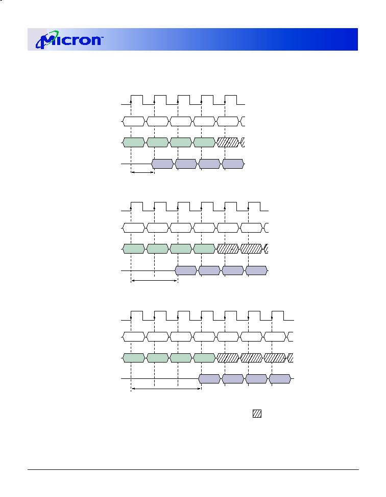
uses a pipelined architecture and therefore does not
require the 2n rule associated with a prefetch architec-
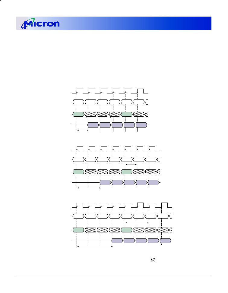
Figure 7
Consecutive READ Bursts
ture. A READ command can be initiated on any clock
cycle following a previous READ command. Full-speed
random read accesses can be performed to the same
bank, as shown in Figure 8, or each subsequent READ
may be performed to a different bank.
CLK
DQ
D
OUT
n
T2
T1
T4
T3
T5
T0
COMMAND
ADDRESS
READ
NOP
NOP
NOP
BANK,
COL n
NOP
BANK,
COL b
D
OUT
n + 1
D
OUT
n + 2
D
OUT
n + 3
D
OUT
b
READ
X = 0 cycles
NOTE: Each READ command may be to either bank. DQM is LOW.
CAS Latency = 1
CLK
DQ
D
OUT
n
T2
T1
T4
T3
T6
T5
T0
COMMAND
ADDRESS
READ
NOP
NOP
NOP
NOP
BANK,
COL n
NOP
BANK,
COL b
D
OUT
n + 1
D
OUT
n + 2
D
OUT
n + 3
D
OUT
b
READ
X = 1 cycle
CAS Latency = 2
CLK
DQ
D
OUT
n
T2
T1
T4
T3
T6
T5
T0
COMMAND
ADDRESS
READ
NOP
NOP
NOP
NOP
BANK,
COL n
NOP
BANK,
COL b
D
OUT
n + 1
D
OUT
n + 2
D
OUT
n + 3
D
OUT
b
READ
NOP
T7
X = 2 cycles
CAS Latency = 3
DON'T CARE
20
128Mb: x16, x32 Mobile SDRAM
Micron Technology, Inc., reserves the right to change products or specifications without notice.
MobileY95W_3V_F.p65 � Rev. F; Pub. 9/02
�2002, Micron Technology, Inc.
128Mb: x16, x32
MOBILE SDRAM
ADVANCE
Figure 8
Random READ Accesses
CLK
DQ
T2
T1
T4
T3
T6
T5
T0
COMMAND
ADDRESS
READ
NOP
NOP
BANK,
COL n
DON'T CARE
D
OUT
n
D
OUT
a
D
OUT
x
D
OUT
m
READ
NOTE: Each READ command may be to either bank. DQM is LOW.
READ
READ
NOP
BANK,
COL a
BANK,
COL x
BANK,
COL m
CLK
DQ
D
OUT
n
T2
T1
T4
T3
T5
T0
COMMAND
ADDRESS
READ
NOP
BANK,
COL n
D
OUT
a
D
OUT
x
D
OUT
m
READ
READ
READ
NOP
BANK,
COL a
BANK,
COL x
BANK,
COL m
CLK
DQ
D
OUT
n
T2
T1
T4
T3
T0
COMMAND
ADDRESS
READ
NOP
BANK,
COL n
D
OUT
a
D
OUT
x
D
OUT
m
READ
READ
READ
BANK,
COL a
BANK,
COL x
BANK,
COL m
CAS Latency = 1
CAS Latency = 2
CAS Latency = 3
21
128Mb: x16, x32 Mobile SDRAM
Micron Technology, Inc., reserves the right to change products or specifications without notice.
MobileY95W_3V_F.p65 � Rev. F; Pub. 9/02
�2002, Micron Technology, Inc.
128Mb: x16, x32
MOBILE SDRAM
ADVANCE
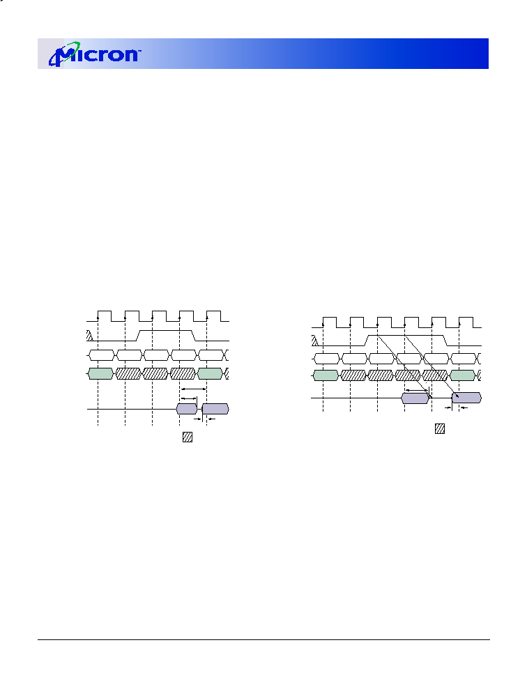
Data from any READ burst may be truncated with a
subsequent WRITE command, and data from a fixed-
length READ burst may be immediately followed by data
from a WRITE command (subject to bus turnaround
limitations). The WRITE burst may be initiated on the
clock edge immediately following the last (or last de-
sired) data element from the READ burst, provided that I/
O contention can be avoided. In a given system design,
there may be a possibility that the device driving the
input data will go Low-Z before the SDRAM DQs go High-
Z. In this case, at least a single-cycle delay should occur
between the last read data and the WRITE command.
The DQM input is used to avoid I/O contention, as
shown in Figures 9 and 10. The DQM signal must be
asserted (HIGH) at least two clocks prior to the WRITE
command (DQM latency is two clocks for output buffers)
DON'T CARE
READ
NOP
NOP
NOP
NOP
DQM
CLK
DQ
D
OUT
n
T2
T1
T4
T3
T0
COMMAND
ADDRESS
BANK,
COL n
WRITE
D
IN
b
BANK,
COL b
T5
DS
tHZ
t
NOTE:
A CAS latency of three is used for illustration. The READ command
may be to any bank, and the WRITE command may be to any bank.
Figure 10
READ to WRITE With
Extra Clock Cycle
Figure 9
READ to WRITE
DON'T CARE
READ
NOP
NOP
WRITE
NOP
CLK
T2
T1
T4
T3
T0
DQM
DQ
D
OUT
n
COMMAND
D
IN
b
ADDRESS
BANK,
COL n
BANK,
COL b
DS
tHZ
t
tCK
NOTE:
A CAS latency of three is used for illustration. The READ
command may be to any bank, and the WRITE command
to suppress data-out from the READ. Once the WRITE
command is registered, the DQs will go High-Z (or re-
main High-Z), regardless of the state of the DQM signal,
provided the DQM was active on the clock just prior to
the WRITE command that truncated the READ com-
mand. If not, the second WRITE will be an invalid WRITE.
For example, if DQM was LOW during T4 in Figure 10,
then the WRITEs at T5 and T7 would be valid, while the
WRITE at T6 would be invalid.
The DQM signal must be de-asserted prior to the
WRITE command (DQM latency is zero clocks for input
buffers) to ensure that the written data is not masked.
Figure 9 shows the case where the clock frequency allows
for bus contention to be avoided without adding a NOP
cycle, and Figure 10 shows the case where the additional
NOP is needed.
22
128Mb: x16, x32 Mobile SDRAM
Micron Technology, Inc., reserves the right to change products or specifications without notice.
MobileY95W_3V_F.p65 � Rev. F; Pub. 9/02
�2002, Micron Technology, Inc.
128Mb: x16, x32
MOBILE SDRAM
ADVANCE
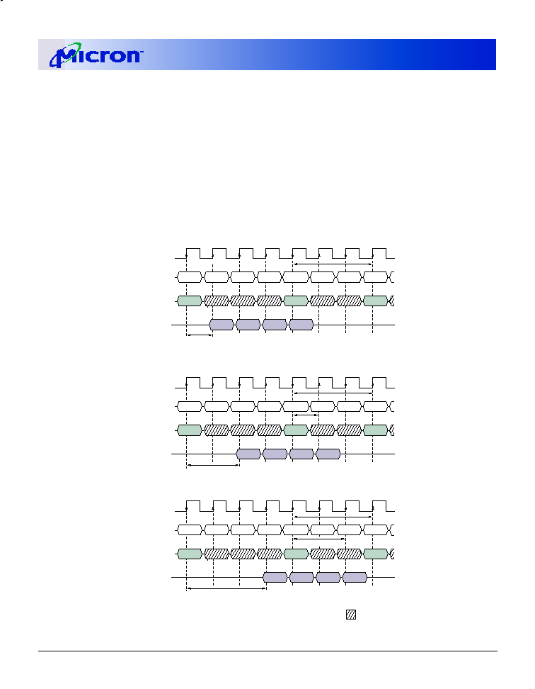
Figure 11
READ to PRECHARGE
A fixed-length READ burst may be followed by, or
truncated with, a PRECHARGE command to the same
bank (provided that auto precharge was not activated),
and a full-page burst may be truncated with a
PRECHARGE command to the same bank. The
PRECHARGE command should be issued x cycles before
the clock edge at which the last desired data element is
valid, where x equals the CAS latency minus one. This is
shown in Figure 11 for each possible CAS latency; data
element n + 3 is either the last of a burst of four or the last
desired of a longer burst. Following the PRECHARGE
command, a subsequent command to the same bank
cannot be issued until
t
RP is met. Note that part of the row
precharge time is hidden during the access of the last
data element(s).
In the case of a fixed-length burst being executed to
completion, a PRECHARGE command issued at the opti-
mum time (as described above) provides the same op-
eration that would result from the same fixed-length
burst with auto precharge. The disadvantage of the
CLK
DQ
D
OUT
n
T2
T1
T4
T3
T6
T5
T0
COMMAND
ADDRESS
READ
NOP
NOP
NOP
NOP
NOP
D
OUT
n + 1
D
OUT
n + 2
D
OUT
n + 3
PRECHARGE
ACTIVE
t RP
T7
NOTE: DQM is LOW.
CLK
DQ
D
OUT
n
T2
T1
T4
T3
T6
T5
T0
COMMAND
ADDRESS
READ
NOP
NOP
NOP
NOP
NOP
D
OUT
n + 1
D
OUT
n + 2
D
OUT
n + 3
PRECHARGE
ACTIVE
t RP
T7
CLK
DQ
D
OUT
n
T2
T1
T4
T3
T6
T5
T0
COMMAND
ADDRESS
READ
NOP
NOP
NOP
NOP
BANK a,
COL n
NOP
D
OUT
n + 1
D
OUT
n + 2
D
OUT
n + 3
PRECHARGE
ACTIVE
t RP
T7
BANK a,
ROW
BANK
(a or all)
DON'T CARE
X = 0 cycles
CAS Latency = 1
X = 1 cycle
CAS Latency = 2
CAS Latency = 3
BANK a,
COL n
BANK a,
ROW
BANK
(a or all)
BANK a,
COL n
BANK a,
ROW
BANK
(a or all)
X = 2 cycles
23
128Mb: x16, x32 Mobile SDRAM
Micron Technology, Inc., reserves the right to change products or specifications without notice.
MobileY95W_3V_F.p65 � Rev. F; Pub. 9/02
�2002, Micron Technology, Inc.
128Mb: x16, x32
MOBILE SDRAM
ADVANCE
Figure 12
Terminating a READ Burst
PRECHARGE command is that it requires that the com-
mand and address buses be available at the appropriate
time to issue the command; the advantage of the
PRECHARGE command is that it can be used to truncate
fixed-length or full-page bursts.
Full-page READ bursts can be truncated with the
BURST TERMINATE command, and fixed-length READ
bursts may be truncated with a BURST TERMINATE com-
mand, provided that auto precharge was not activated.
The BURST TERMINATE command should be issued x
cycles before the clock edge at which the last desired data
element is valid, where x equals the CAS latency minus
one. This is shown in Figure 12 for each possible CAS
latency; data element n + 3 is the last desired data ele-
ment of a longer burst.
DON'T CARE
CLK
DQ
D
OUT
n
T2
T1
T4
T3
T6
T5
T0
COMMAND
ADDRESS
READ
NOP
NOP
NOP
NOP
BANK,
COL n
NOP
D
OUT
n + 1
D
OUT
n + 2
D
OUT
n + 3
BURST
TERMINATE
NOP
T7
NOTE: DQM is LOW.
CLK
DQ
D
OUT
n
T2
T1
T4
T3
T6
T5
T0
COMMAND
ADDRESS
READ
NOP
NOP
NOP
BANK,
COL n
NOP
D
OUT
n + 1
D
OUT
n + 2
D
OUT
n + 3
BURST
TERMINATE
NOP
CLK
DQ
D
OUT
n
T2
T1
T4
T3
T6
T5
T0
COMMAND
ADDRESS
READ
NOP
NOP
NOP
BANK,
COL n
NOP
D
OUT
n + 1
D
OUT
n + 2
D
OUT
n + 3
BURST
TERMINATE
NOP
X = 0 cycles
CAS Latency = 1
X = 1 cycle
CAS Latency = 2
CAS Latency = 3
X = 2 cycles
24
128Mb: x16, x32 Mobile SDRAM
Micron Technology, Inc., reserves the right to change products or specifications without notice.
MobileY95W_3V_F.p65 � Rev. F; Pub. 9/02
�2002, Micron Technology, Inc.
128Mb: x16, x32
MOBILE SDRAM
ADVANCE
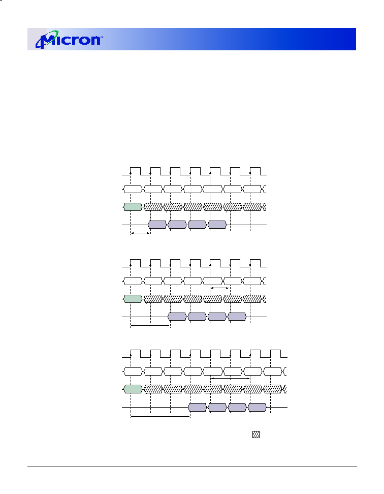
WRITEs
WRITE bursts are initiated with a WRITE command,
as shown in Figure 13.
The starting column and bank addresses are pro-
vided with the WRITE command, and auto precharge is
either enabled or disabled for that access. If auto
precharge is enabled, the row being accessed is
precharged at the completion of the burst. For the ge-
neric WRITE commands used in the following illustra-
tions, auto precharge is disabled.
During WRITE bursts, the first valid data-in element
will be registered coincident with the WRITE command.
Subsequent data elements will be registered on each
successive positive clock edge. Upon completion of a
fixed-length burst, assuming no other commands have
been initiated, the DQs will remain High-Z and any addi-
tional input data will be ignored (see Figure 14). A full-
page burst will continue until terminated. (At the end of
the page, it will wrap to column 0 and continue.)
Data for any WRITE burst may be truncated with a
subsequent WRITE command, and data for a fixed-length
WRITE burst may be immediately followed by data for a
WRITE command. The new WRITE command can be
issued on any clock following the previous WRITE com-
mand, and the data provided coincident with the new
Figure 15
WRITE to WRITE
command applies to the new command. An example is
shown in Figure 15. Data n + 1 is either the last of a burst
of two or the last desired of a longer burst. The 128Mb
SDRAM uses a pipelined architecture and therefore does
not require the 2n rule associated with a prefetch archi-
tecture. A WRITE command can be initiated on any clock
cycle following a previous WRITE command. Full-speed
random write accesses within a page can be performed to
the same bank, as shown in Figure 16, or each subsequent
WRITE may be performed to a different bank.
CLK
DQ
D
IN
n
T2
T1
T3
T0
COMMAND
ADDRESS
NOP
NOP
WRITE
D
IN
n + 1
NOP
BANK,
COL n
NOTE:
Burst length = 2. DQM is LOW.
Figure 14
WRITE Burst
DON'T CARE
CLK
DQ
T2
T1
T0
COMMAND
ADDRESS
NOP
WRITE
WRITE
BANK,
COL n
BANK,
COL b
D
IN
n
D
IN
n + 1
D
IN
b
NOTE:
DQM is LOW. Each WRITE
command may be to any bank.
Figure 13
WRITE Command
CS#
WE#
CAS#
RAS#
CKE
CLK
COLUMN
ADDRESS
DON'T CARE
HIGH
ENABLE AUTO PRECHARGE
DISABLE AUTO PRECHARGE
BANK
ADDRESS
A0-A8
A10
BA0,1
A9, A11
VALID ADDRESS

25
128Mb: x16, x32 Mobile SDRAM
Micron Technology, Inc., reserves the right to change products or specifications without notice.
MobileY95W_3V_F.p65 � Rev. F; Pub. 9/02
�2002, Micron Technology, Inc.
128Mb: x16, x32
MOBILE SDRAM
ADVANCE
least one clock plus time, regardless of frequency.
In addition, when truncating a WRITE burst, the DQM
signal must be used to mask input data for the clock edge
prior to, and the clock edge coincident with, the
PRECHARGE command. An example is shown in Figure
18. Data n + 1 is either the last of a burst of two or the last
desired of a longer burst. Following the PRECHARGE
command, a subsequent command to the same bank
cannot be issued until
t
RP is met.
In the case of a fixed-length burst being executed to
completion, a PRECHARGE command issued at the opti-
mum time (as described above) provides the same op-
eration that would result from the same fixed-length
burst with auto precharge. The disadvantage of the
PRECHARGE command is that it requires that the com-
mand and address buses be available at the appropriate
time to issue the command; the advantage of the
PRECHARGE command is that it can be used to truncate
fixed-length or full-page bursts.
Figure 18
WRITE to PRECHARGE
DQM
CLK
DQ
T2
T1
T4
T3
T0
COMMAND
ADDRESS
BANK a,
COL n
T5
NOP
WRITE
PRECHARGE
NOP
NOP
D
IN
n
D
IN
n + 1
ACTIVE
t RP
BANK
(a or all)
t WR
BANK a,
ROW
DQM
DQ
COMMAND
ADDRESS
BANK a,
COL n
NOP
WRITE
PRECHARGE
NOP
NOP
D
IN
n
D
IN
n + 1
ACTIVE
t RP
DON'T CARE
BANK
(a or all)
t WR
NOTE:
DQM could remain LOW in this example if the WRITE burst is a fixed length
of two.
BANK a,
ROW
T6
NOP
NOP
t
WR@
t
CK 15ns
t
WR@
t
CK < 15ns
Data for any WRITE burst may be truncated with a
subsequent READ command, and data for a fixed-length
WRITE burst may be immediately followed by a READ
command. Once the READ command is registered, the
data inputs will be ignored, and WRITEs will not be
executed. An example is shown in Figure 17. Data n + 1 is
either the last of a burst of two or the last desired of a
longer burst.
Data for a fixed-length WRITE burst may be followed
by, or truncated with, a PRECHARGE command to the
same bank (provided that auto precharge was not acti-
vated), and a full-page WRITE burst may be truncated
with a PRECHARGE command to the same bank. The
PRECHARGE command should be issued
t
WR after the
clock edge at which the last desired input data element is
registered. The auto precharge mode requires a
t
WR of at
Figure 17
WRITE to READ
CLK
DQ
T2
T1
T3
T0
COMMAND
ADDRESS
NOP
WRITE
BANK,
COL n
D
IN
n
D
IN
n + 1
D
OUT
b
READ
NOP
NOP
BANK,
COL b
NOP
D
OUT
b + 1
T4
T5
NOTE:
The WRITE command may be to any bank, and the READ command may
be to any bank. DQM is LOW. CAS latency = 2 for illustration.
Figure 16
Random WRITE Cycles
CLK
DQ
D
IN
n
T2
T1
T3
T0
COMMAND
ADDRESS
WRITE
BANK,
COL n
D
IN
a
D
IN
x
D
IN
m
WRITE
WRITE
WRITE
BANK,
COL a
BANK,
COL x
BANK,
COL m
NOTE:
Each WRITE command may be to any bank.
DQM is LOW.
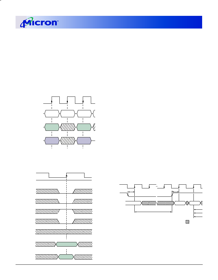
26
128Mb: x16, x32 Mobile SDRAM
Micron Technology, Inc., reserves the right to change products or specifications without notice.
MobileY95W_3V_F.p65 � Rev. F; Pub. 9/02
�2002, Micron Technology, Inc.
128Mb: x16, x32
MOBILE SDRAM
ADVANCE
Fixed-length or full-page WRITE bursts can be trun-
cated with the BURST TERMINATE command. When
truncating a WRITE burst, the input data applied coinci-
dent with the BURST TERMINATE command will be
ignored. The last data written (provided that DQM is
LOW at that time) will be the input data applied one clock
previous to the BURST TERMINATE command. This is
shown in Figure 19, where data n is the last desired data
element of a longer burst.
Figure 21
Power-Down
DON'T CARE
tRAS
tRCD
tRC
All banks idle
Input buffers gated off
Exit power-down mode.
(
)
(
)
(
)
(
)
(
)
(
)
tCKS
> tCKS
COMMAND
NOP
ACTIVE
Enter power-down mode.
NOP
CLK
CKE
(
)
(
)
(
)
(
)
Figure 20
PRECHARGE Command
Figure 19
Terminating a WRITE Burst
CS#
WE#
CAS#
RAS#
CKE
CLK
A10
HIGH
All Banks
Bank Selected
A0-A9
BA0,1
BANK
ADDRESS
CLK
DQ
T2
T1
T0
COMMAND
ADDRESS
BANK,
COL n
WRITE
BURST
TERMINATE
NEXT
COMMAND
D
IN
n
(ADDRESS)
(DATA)
PRECHARGE
The PRECHARGE command (see Figure 20) is used to
deactivate the open row in a particular bank or the open
row in all banks. The bank(s) will be available for a subse-
quent row access some specified time (
t
RP) after the
PRECHARGE command is issued. Input A10 determines
whether one or all banks are to be precharged, and in the
case where only one bank is to be precharged, inputs
BA0, BA1 select the bank. When all banks are to be
precharged, inputs BA0, BA1 are treated as "Don't Care."
Once a bank has been precharged, it is in the idle state
and must be activated prior to any READ or WRITE com-
mands being issued to that bank.
POWER-DOWN
Power-down occurs if CKE is registered LOW coinci-
dent with a NOP or COMMAND INHIBIT when no ac-
cesses are in progress. If power-down occurs when all
banks are idle, this mode is referred to as precharge
power-down; if power-down occurs when there is a row
active in any bank, this mode is referred to as active
power-down. Entering power-down deactivates the in-
put and output buffers, excluding CKE, for maximum
power savings while in standby. The device may not
remain in the power-down state longer than the refresh
period (64ms) since no refresh operations are performed
in this mode.
The power-down state is exited by registering a NOP
or COMMAND INHIBIT and CKE HIGH at the desired
clock edge (meeting
t
CKS). See Figure 21.
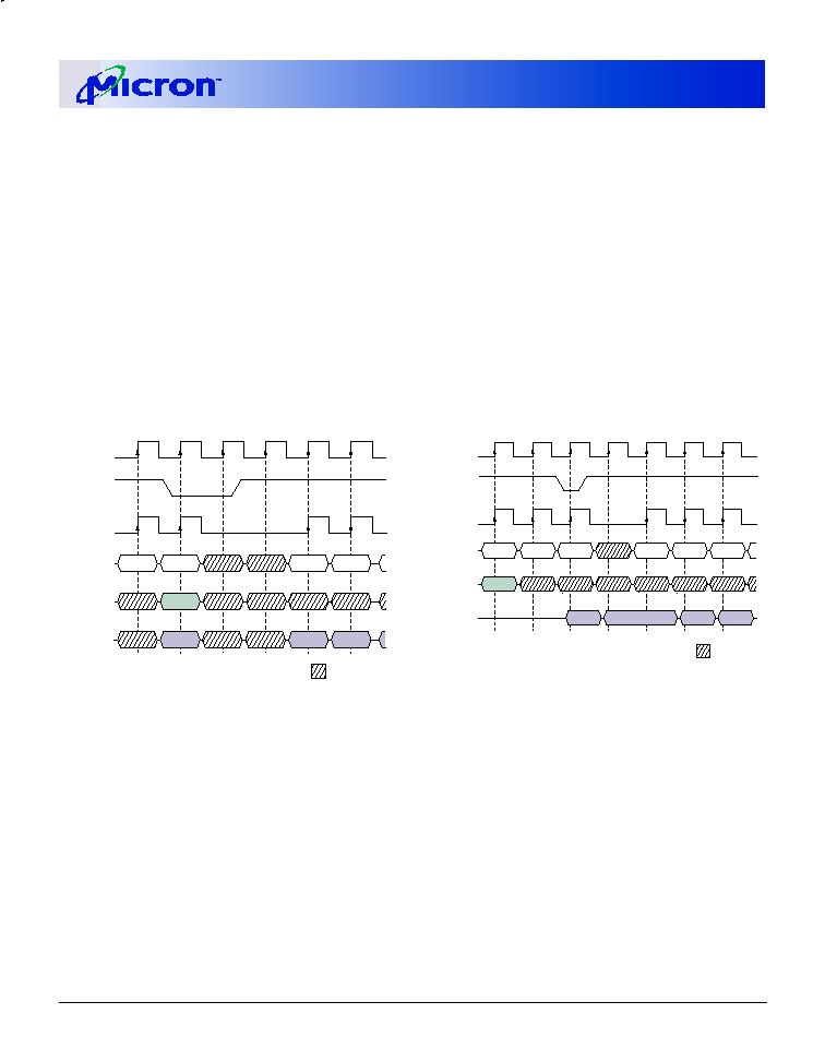
27
128Mb: x16, x32 Mobile SDRAM
Micron Technology, Inc., reserves the right to change products or specifications without notice.
MobileY95W_3V_F.p65 � Rev. F; Pub. 9/02
�2002, Micron Technology, Inc.
128Mb: x16, x32
MOBILE SDRAM
ADVANCE
DON'T CARE
D
IN
COMMAND
ADDRESS
WRITE
BANK,
COL n
D
IN
n
NOP
NOP
CLK
T2
T1
T4
T3
T5
T0
CKE
INTERNAL
CLOCK
NOP
D
IN
n + 1
D
IN
n + 2
Figure 22
Clock Suspend During WRITE Burst
DON'T CARE
CLK
DQ
D
OUT
n
T2
T1
T4
T3
T6
T5
T0
COMMAND
ADDRESS
READ
NOP
NOP
NOP
BANK,
COL n
NOP
D
OUT
n + 1
D
OUT
n + 2
D
OUT
n + 3
NOTE: For this example, CAS latency = 2, burst length = 4 or greater, and
DQM is LOW.
CKE
INTERNAL
CLOCK
NOP
Figure 23
Clock Suspend During READ Burst
CLOCK SUSPEND
The clock suspend mode occurs when a column ac-
cess/burst is in progress and CKE is registered LOW. In
the clock suspend mode, the internal clock is deacti-
vated, "freezing" the synchronous logic.
For each positive clock edge on which CKE is sampled
LOW, the next internal positive clock edge is suspended.
Any command or data present on the input pins at the
time of a suspended internal clock edge is ignored; any
data present on the DQ pins remains driven; and burst
counters are not incremented, as long as the clock is
suspended. (See examples in Figures 22 and 23.)
Clock suspend mode is exited by registering CKE
HIGH; the internal clock and related operation will re-
sume on the subsequent positive clock edge.
BURST READ/SINGLE WRITE
The burst read/single write mode is entered by pro-
gramming the write burst mode bit (M9) in the mode
register to a logic 1. In this mode, all WRITE commands
result in the access of a single column location (burst of
one), regardless of the programmed burst length. READ
commands access columns according to the programmed
burst length and sequence, just as in the normal mode of
operation (M9 = 0).
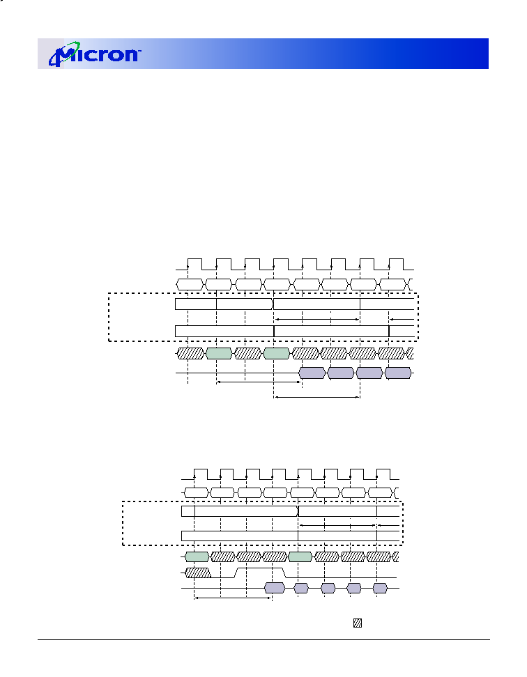
28
128Mb: x16, x32 Mobile SDRAM
Micron Technology, Inc., reserves the right to change products or specifications without notice.
MobileY95W_3V_F.p65 � Rev. F; Pub. 9/02
�2002, Micron Technology, Inc.
128Mb: x16, x32
MOBILE SDRAM
ADVANCE
CONCURRENT AUTO PRECHARGE
An access command (READ or WRITE) to another
bank while an access command with auto precharge
enabled is executing is not allowed by SDRAMs, unless
the SDRAM supports CONCURRENT AUTO PRECHARGE.
Micron SDRAMs support CONCURRENT AUTO
PRECHARGE. Four cases where CONCURRENT AUTO
PRECHARGE occurs are defined below.
READ with Auto Precharge
1. Interrupted by a READ (with or without auto
precharge): A READ to bank m will interrupt a READ
on bank n, CAS latency later. The PRECHARGE to
bank n will begin when the READ to bank m is regis-
tered (Figure 24).
2. Interrupted by a WRITE (with or without auto
precharge): A WRITE to bank m will interrupt a READ
on bank n when registered. DQM should be used two
clocks prior to the WRITE command to prevent bus
contention. The PRECHARGE to bank n will begin
when the WRITE to bank m is registered (Figure 25).
CLK
DQ
D
OUT
a
T2
T1
T4
T3
T6
T5
T0
COMMAND
READ - AP
BANK n
NOP
NOP
NOP
NOP
D
OUT
a + 1
D
OUT
d
D
OUT
d + 1
NOP
T7
BANK n
CAS Latency = 3 (BANK m)
BANK m
ADDRESS
Idle
NOP
NOTE: DQM is LOW.
BANK n,
COL a
BANK m,
COL d
READ - AP
BANK m
Internal
States
t
Page Active
READ with Burst of 4
Interrupt Burst, Precharge
Page Active
READ with Burst of 4
Precharge
RP - BANK n
tRP - BANK m
CAS Latency = 3 (BANK n)
Figure 24
READ With Auto Precharge Interrupted by a READ
CLK
DQ
D
OUT
a
T2
T1
T4
T3
T6
T5
T0
COMMAND
NOP
NOP
NOP
NOP
D
IN
d + 1
D
IN
d
D
IN
d + 2
D
IN
d + 3
NOP
T7
BANK n
BANK m
ADDRESS
Idle
NOP
DQM
NOTE: 1. DQM is HIGH at T2 to prevent D
OUT
-a+1 from contending with D
IN
-d at T4.
BANK n,
COL a
BANK m,
COL d
WRITE - AP
BANK m
Internal
States
t
Page
Active
READ with Burst of 4
Interrupt Burst, Precharge
Page Active
WRITE with Burst of 4
Write-Back
RP - BANK n
t WR - BANK m
CAS Latency = 3 (BANK n)
READ - AP
BANK n
1
DON'T CARE
Figure 25
READ With Auto Precharge Interrupted by a WRITE
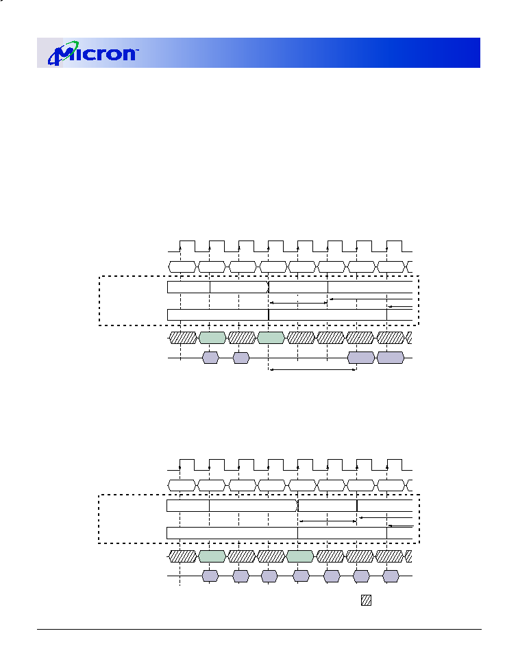
29
128Mb: x16, x32 Mobile SDRAM
Micron Technology, Inc., reserves the right to change products or specifications without notice.
MobileY95W_3V_F.p65 � Rev. F; Pub. 9/02
�2002, Micron Technology, Inc.
128Mb: x16, x32
MOBILE SDRAM
ADVANCE
CLK
DQ
T2
T1
T4
T3
T6
T5
T0
COMMAND
WRITE - AP
BANK n
NOP
NOP
NOP
NOP
D
IN
a + 1
D
IN
a
NOP
NOP
T7
BANK n
BANK m
ADDRESS
NOTE: 1. DQM is LOW.
BANK n,
COL a
BANK m,
COL d
READ - AP
BANK m
Internal
States
t
Page Active
WRITE with Burst of 4
Interrupt Burst, Write-Back
Precharge
Page Active
READ with Burst of 4
t
tRP - BANK m
D
OUT
d
D
OUT
d + 1
CAS Latency = 3 (BANK m)
RP - BANK n
WR - BANK n
Figure 26
WRITE With Auto Precharge Interrupted by a READ
DON'T CARE
CLK
DQ
T2
T1
T4
T3
T6
T5
T0
COMMAND
WRITE - AP
BANK n
NOP
NOP
NOP
NOP
D
IN
d + 1
D
IN
d
D
IN
a + 1
D
IN
a + 2
D
IN
a
D
IN
d + 2
D
IN
d + 3
NOP
T7
BANK n
BANK m
ADDRESS
NOP
NOTE: 1. DQM is LOW.
BANK n,
COL a
BANK m,
COL d
WRITE - AP
BANK m
Internal
States
t
Page Active
WRITE with Burst of 4
Interrupt Burst, Write-Back
Precharge
Page Active
WRITE with Burst of 4
Write-Back
WR - BANK n
tRP - BANK n
t WR - BANK m
Figure 27
WRITE With Auto Precharge Interrupted by a WRITE
WRITE with Auto Precharge
3. Interrupted by a READ (with or without auto
precharge): A READ to bank m will interrupt a WRITE
on bank n when registered, with the data-out appear-
ing CAS latency later. The PRECHARGE to bank n will
begin after
t
WR is met, where
t
WR begins when the
READ to bank m is registered. The last valid WRITE to
bank n will be data-in registered one clock prior to the
READ to bank m (Figure 26).
4. Interrupted by a WRITE (with or without auto
precharge): A WRITE to bank m will interrupt a WRITE
on bank n when registered. The PRECHARGE to bank
n will begin after
t
WR is met, where
t
WR begins when
the WRITE to bank m
is registered.
The last valid data WRITE to bank n will be data
registered one clock prior to a WRITE to bank m
(Figure 27).

30
128Mb: x16, x32 Mobile SDRAM
Micron Technology, Inc., reserves the right to change products or specifications without notice.
MobileY95W_3V_F.p65 � Rev. F; Pub. 9/02
�2002, Micron Technology, Inc.
128Mb: x16, x32
MOBILE SDRAM
ADVANCE
TRUTH TABLE 2 � CKE
(Notes: 1-4)
CKE
n-1
CKE
n
CURRENT STATE
COMMAND
n
ACTION
n
NOTES
L
L
Power-Down
X
Maintain Power-Down
Self Refresh
X
Maintain Self Refresh
Clock Suspend
X
Maintain Clock Suspend
L
H
Power-Down
COMMAND INHIBIT or NOP
Exit Power-Down
5
Self Refresh
COMMAND INHIBIT or NOP
Exit Self Refresh
6
Clock Suspend
X
Exit Clock Suspend
7
H
L
All Banks Idle
COMMAND INHIBIT or NOP
Power-Down Entry
All Banks Idle
AUTO REFRESH
Self Refresh Entry
Reading or Writing
VALID
Clock Suspend Entry
H
H
See Truth Table 3
NOTE: 1. CKE
n
is the logic state of CKE at clock edge n; CKE
n-1
was the state of CKE at the previous clock edge.
2. Current state is the state of the SDRAM immediately prior to clock edge n.
3. COMMAND
n
is the command registered at clock edge n, and ACTION
n
is a result of COMMAND
n
.
4. All states and sequences not shown are illegal or reserved.
5. Exiting power-down at clock edge n will put the device in the all banks idle state in time for clock edge n + 1
(provided that
t
CKS is met).
6. Exiting self refresh at clock edge n will put the device in the all banks idle state once
t
XSR is met. COMMAND INHIBIT
or NOP commands should be issued on any clock edges occurring during the
t
XSR period. A minimum of two NOP
commands must be provided during
t
XSR period.
7. After exiting clock suspend at clock edge n, the device will resume operation and recognize the next command at
clock edge n + 1.

31
128Mb: x16, x32 Mobile SDRAM
Micron Technology, Inc., reserves the right to change products or specifications without notice.
MobileY95W_3V_F.p65 � Rev. F; Pub. 9/02
�2002, Micron Technology, Inc.
128Mb: x16, x32
MOBILE SDRAM
ADVANCE
TRUTH TABLE 3 � CURRENT STATE BANK n, COMMAND TO BANK n
(Notes: 1-6; notes appear below and on next page)
CURRENT STATE CS# RAS# CAS# WE#
COMMAND (ACTION)
NOTES
Any
H
X
X
X
COMMAND INHIBIT (NOP/Continue previous operation)
L
H
H
H
NO OPERATION (NOP/Continue previous operation)
L
L
H
H
ACTIVE (Select and activate row)
Idle
L
L
L
H
AUTO REFRESH
7
L
L
L
L
LOAD MODE REGISTER
7
L
L
H
L
PRECHARGE
11
L
H
L
H
READ (Select column and start READ burst)
10
Row Active
L
H
L
L
WRITE (Select column and start WRITE burst)
10
L
L
H
L
PRECHARGE (Deactivate row in bank or banks)
8
Read
L
H
L
H
READ (Select column and start new READ burst)
10
(Auto
L
H
L
L
WRITE (Select column and start WRITE burst)
10
Precharge
L
L
H
L
PRECHARGE (Truncate READ burst, start PRECHARGE)
8
Disabled)
L
H
H
L
BURST TERMINATE
9
Write
L
H
L
H
READ (Select column and start READ burst)
10
(Auto
L
H
L
L
WRITE (Select column and start new WRITE burst)
10
Precharge
L
L
H
L
PRECHARGE (Truncate WRITE burst, start PRECHARGE)
8
Disabled)
L
H
H
L
BURST TERMINATE
9
NOTE: 1. This table applies when CKE
n-1
was HIGH and CKE
n
is HIGH (see Truth Table 2) and after
t
XSR has been
met (if the previous state was self refresh).
2. This table is bank-specific, except where noted; i.e., the current state is for a specific bank and the commands shown
are those allowed to be issued to that bank when in that state. Exceptions are covered in the notes below.
3. Current state definitions:
Idle: The bank has been precharged, and
t
RP has been met.
Row Active: A row in the bank has been activated, and
t
RCD has been met. No data bursts/accesses and
no register accesses are in progress.
Read: A READ burst has been initiated, with auto precharge disabled, and has not yet
terminated or been terminated.
Write: A WRITE burst has been initiated, with auto precharge disabled, and has not yet terminated
or been terminated.
4. The following states must not be interrupted by a command issued to the same bank. COMMAND INHIBIT or NOP
commands, or allowable commands to the other bank should be issued on any clock edge occurring during these
states. Allowable commands to the other bank are determined by its current state and Truth Table 3, and according to
Truth Table 4.
Precharging: Starts with registration of a PRECHARGE command and ends when
t
RP is met. Once
t
RP is
met, the bank will be in the idle state.
Row Activating: Starts with registration of an ACTIVE command and ends when
t
RCD is met. Once
t
RCD is
met, the bank will be in the row active state.
Read w/Auto
Precharge Enabled: Starts with registration of a READ command with auto precharge enabled and ends when
t
RP
has been met. Once
t
RP is met, the bank will be in the idle state.
Write w/Auto
Precharge Enabled: Starts with registration of a WRITE command with auto precharge enabled and ends when
t
RP has been met. Once
t
RP is met, the bank will be in the idle state.
(Continued on next page)

32
128Mb: x16, x32 Mobile SDRAM
Micron Technology, Inc., reserves the right to change products or specifications without notice.
MobileY95W_3V_F.p65 � Rev. F; Pub. 9/02
�2002, Micron Technology, Inc.
128Mb: x16, x32
MOBILE SDRAM
ADVANCE
NOTE (continued):
5. The following states must not be interrupted by any executable command; COMMAND INHIBIT or NOP commands
must be applied on each positive clock edge during these states.
Refreshing: Starts with registration of an AUTO REFRESH command and ends when
t
RC is met. Once
t
RC is
met, the SDRAM will be in the all banks idle state.
Accessing Mode
Register: Starts with registration of a LOAD MODE REGISTER command and ends when
t
MRD has been
met. Once
t
MRD is met, the SDRAM will be in the all banks idle state.
Precharging All: Starts with registration of a PRECHARGE ALL command and ends when
t
RP is met. Once
t
RP is
met, all banks will be in the idle state.
6. All states and sequences not shown are illegal or reserved.
7. Not bank-specific; requires that all banks are idle.
8. May or may not be bank-specific; if all banks are to be precharged, all must be in a valid state for precharging.
9. Not bank-specific; BURST TERMINATE affects the most recent READ or WRITE burst, regardless of bank.
10. READs or WRITEs listed in the Command (Action) column include READs or WRITEs with auto precharge enabled and
READs or WRITEs with auto precharge disabled.
11. Does not affect the state of the bank and acts as a NOP to that bank.
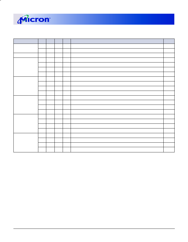
33
128Mb: x16, x32 Mobile SDRAM
Micron Technology, Inc., reserves the right to change products or specifications without notice.
MobileY95W_3V_F.p65 � Rev. F; Pub. 9/02
�2002, Micron Technology, Inc.
128Mb: x16, x32
MOBILE SDRAM
ADVANCE
TRUTH TABLE 4 � CURRENT STATE BANK n, COMMAND TO BANK m
(Notes: 1-6; notes appear below and on next page)
CURRENT STATE CS# RAS# CAS# WE#
COMMAND (ACTION)
NOTES
Any
H
X
X
X
COMMAND INHIBIT (NOP/Continue previous operation)
L
H
H
H
NO OPERATION (NOP/Continue previous operation)
Idle
X
X
X
X
Any Command Otherwise Allowed to Bank m
Row
L
L
H
H
ACTIVE (Select and activate row)
Activating,
L
H
L
H
READ (Select column and start READ burst)
7
Active, or
L
H
L
L
WRITE (Select column and start WRITE burst)
7
Precharging
L
L
H
L
PRECHARGE
Read
L
L
H
H
ACTIVE (Select and activate row)
(Auto
L
H
L
H
READ (Select column and start new READ burst)
7, 10
Precharge
L
H
L
L
WRITE (Select column and start WRITE burst)
7, 11
Disabled)
L
L
H
L
PRECHARGE
9
Write
L
L
H
H
ACTIVE (Select and activate row)
(Auto
L
H
L
H
READ (Select column and start READ burst)
7, 12
Precharge
L
H
L
L
WRITE (Select column and start new WRITE burst)
7, 13
Disabled)
L
L
H
L
PRECHARGE
9
Read
L
L
H
H
ACTIVE (Select and activate row)
(With Auto
L
H
L
H
READ (Select column and start new READ burst)
7, 8, 14
Precharge)
L
H
L
L
WRITE (Select column and start WRITE burst)
7, 8, 15
L
L
H
L
PRECHARGE
9
Write
L
L
H
H
ACTIVE (Select and activate row)
(With Auto
L
H
L
H
READ (Select column and start READ burst)
7, 8, 16
Precharge)
L
H
L
L
WRITE (Select column and start new WRITE burst)
7, 8, 17
L
L
H
L
PRECHARGE
9
NOTE: 1. This table applies when CKE
n-1
was HIGH and CKE
n
is HIGH (see Truth Table 2) and after
t
XSR has been met (if the
previous state was self refresh).
2. This table describes alternate bank operation, except where noted; i.e., the current state is for bank n and the
commands shown are those allowed to be issued to bank m (assuming that bank m is in such a state that the given
command is allowable). Exceptions are covered in the notes below.
3. Current state definitions:
Idle: The bank has been precharged, and
t
RP has been met.
Row Active: A row in the bank has been activated, and
t
RCD has been met. No data bursts/accesses and
no register accesses are in progress.
Read: A READ burst has been initiated, with auto precharge disabled, and has not yet terminated
or been terminated.
Write: A WRITE burst has been initiated, with auto precharge disabled, and has not yet terminated
or been terminated.
Read w/Auto
Precharge Enabled: Starts with registration of a READ command with auto precharge enabled, and ends when
t
RP has been met. Once
t
RP is met, the bank will be in the idle state.
Write w/Auto
Precharge Enabled: Starts with registration of a WRITE command with auto precharge enabled, and ends when
t
RP has been met. Once
t
RP is met, the bank will be in the idle state.
(Continued on next page)

34
128Mb: x16, x32 Mobile SDRAM
Micron Technology, Inc., reserves the right to change products or specifications without notice.
MobileY95W_3V_F.p65 � Rev. F; Pub. 9/02
�2002, Micron Technology, Inc.
128Mb: x16, x32
MOBILE SDRAM
ADVANCE
NOTE (continued):
4. AUTO REFRESH, SELF REFRESH and LOAD MODE REGISTER commands may only be issued when all banks are idle.
5. A BURST TERMINATE command cannot be issued to another bank; it applies to the bank represented by the current
state only.
6. All states and sequences not shown are illegal or reserved.
7. READs or WRITEs to bank m listed in the Command (Action) column include READs or WRITEs with auto precharge
enabled and READs or WRITEs with auto precharge disabled.
8. CONCURRENT AUTO PRECHARGE: Bank n will initiate the auto precharge command when its burst has been
interrupted by bank m's burst.
9. Burst in bank n continues as initiated.
10. For a READ without auto precharge interrupted by a READ (with or without auto precharge), the READ to bank m
will interrupt the READ on bank n, CAS latency later (Figure 7).
11. For a READ without auto precharge interrupted by a WRITE (with or without auto precharge), the WRITE to bank m
will interrupt the READ on bank n when registered (Figures 9 and 10). DQM should be used one clock prior to the
WRITE command to prevent bus contention.
12. For a WRITE without auto precharge interrupted by a READ (with or without auto precharge), the READ to bank m
will interrupt the WRITE on bank n when registered (Figure 17), with the data-out appearing CAS latency later. The
last valid WRITE to bank n will be data-in registered one clock prior to the READ to bank m.
13. For a WRITE without auto precharge interrupted by a WRITE (with or without auto precharge), the WRITE to bank m
will interrupt the WRITE on bank n when registered (Figure 15). The last valid WRITE to bank n will be data-in
registered one clock prior to the READ to bank m.
14. For a READ with auto precharge interrupted by a READ (with or without auto precharge), the READ to bank m will
interrupt the READ on bank n, CAS latency later. The PRECHARGE to bank n will begin when the READ to bank m is
registered (Figure 24).
15. For a READ with auto precharge interrupted by a WRITE (with or without auto precharge), the WRITE to bank m will
interrupt the READ on bank n when registered. DQM should be used two clocks prior to the WRITE command to
prevent bus contention. The PRECHARGE to bank n will begin when the WRITE to bank m is registered (Figure 25).
16. For a WRITE with auto precharge interrupted by a READ (with or without auto precharge), the READ to bank m will
interrupt the WRITE on bank n when registered, with the data-out appearing CAS latency later. The PRECHARGE to
bank n will begin after
t
WR is met, where
t
WR begins when the READ to bank m is registered. The last valid WRITE to
bank n will be data-in registered one clock prior to the READ to bank m (Figure 26).
17. For a WRITE with auto precharge interrupted by a WRITE (with or without auto precharge), the WRITE to bank m will
interrupt the WRITE on bank n when registered. The PRECHARGE to bank n will begin after
t
WR is met, where
t
WR
begins when the WRITE to bank m is registered. The last valid WRITE to bank n will be data registered one clock prior
to the WRITE to bank m (Figure 27).
35
128Mb: x16, x32 Mobile SDRAM
Micron Technology, Inc., reserves the right to change products or specifications without notice.
MobileY95W_3V_F.p65 � Rev. F; Pub. 9/02
�2002, Micron Technology, Inc.
128Mb: x16, x32
MOBILE SDRAM
ADVANCE
DC ELECTRICAL CHARACTERISTICS AND OPERATING CONDITIONS - LC VERSION
(Notes: 1, 5, 6; notes appear on page 39; V
DD
= +3.3V �0.3V, V
DD
Q = +3.3V �0.3V
PARAMETER/CONDITION
SYMBOL
MIN
MAX
UNITS NOTES
Supply Voltage
V
DD
3
3.6
V
I/O Supply Voltage
V
DD
Q
3
3.6
V
Input High Voltage: Logic 1; All inputs
V
IH
2
V
DD
+ 0.3
V
22
Input Low Voltage: Logic 0; All inputs
V
IL
-0.3
0.8
V
22
Data Output High Voltage: Logic 1; All inputs
V
OH
2.4
�
V
Data Output LOW Voltage: LOGIC 0; All inputs
V
OL
�
0.4
V
Input Leakage Current:
I
I
-5
5
�A
Any Input 0V
V
IN
V
DD
(All other pins not under test = 0V)
Output Leakage Current: DQs are disabled; 0V
V
OUT
V
DD
Q
I
OZ
-5
5
�A
DC ELECTRICAL CHARACTERISTICS AND OPERATING CONDITIONS - V VERSION
(Notes: 1, 5, 6; notes appear on page 39; V
DD
= 2.5 �0.2V, V
DD
Q = +2.5V �0.2V or +1.8V �0.15V )
PARAMETER/CONDITION
SYMBOL
MIN
MAX
UNITS NOTES
Supply Voltage
V
DD
2.3
2.7
V
I/O Supply Voltage
V
DD
Q(2.5V)
2.3
2.7
V
V
DD
Q(1.8V)
1.65
1.95
V
Input High Voltage: Logic 1; All inputs
V
IH
1.25
V
DD
+ 0.3
V
22
Input Low Voltage: Logic 0; All inputs
V
IL
-0.3
+0.55
V
22
Data Output High Voltage: Logic 1; All inputs
V
OH
V
DD
Q - 0.2
�
V
Data Output Low Voltage: LOGIC 0; All inputs
V
OL
�
0.2
V
Input Leakage Current:
I
I
-2
2
�A
Any input 0V
V
IN
V
DD
(All other pins not under test = 0V)
Output Leakage Current: DQs are disabled; 0V
V
OUT
V
DD
Q
I
OZ
-5
5
�A
ABSOLUTE MAXIMUM RATINGS*
Voltage on V
DD
/V
DD
Q Supply
Relative to V
SS
(3.3V) ............................. -1V to +4.6V
Relative to V
SS
(2.5V) ......................... -0.5V to +3.6V
Voltage on Inputs, NC or I/O Pins
Relative to V
SS
(3.3V) ............................. -1V to +4.6V
Relative to V
SS
(2.5V) ......................... -0.5V to +3.6V
Operating Temperature,
T
A
(Industrial) ....................................... -40�C to +85�C
Storage Temperature (plastic) ................ -55�C to +150�C
Power Dissipation .......................................................... 1W
*Stresses greater than those listed under "Absolute Maxi-
mum Ratings" may cause permanent damage to the de-
vice. This is a stress rating only, and functional operation
of the device at these or any other conditions above those
indicated in the operational sections of this specification
is not implied. Exposure to absolute maximum rating
conditions for extended periods may affect reliability.
36
128Mb: x16, x32 Mobile SDRAM
Micron Technology, Inc., reserves the right to change products or specifications without notice.
MobileY95W_3V_F.p65 � Rev. F; Pub. 9/02
�2002, Micron Technology, Inc.
128Mb: x16, x32
MOBILE SDRAM
ADVANCE
ELECTRICAL CHARACTERISTICS AND RECOMMENDED AC OPERATING CONDITIONS
(Notes: 5, 6, 8, 9, 11; notes appear on page 39)
AC CHARACTERISTICS
-8
-10
PARAMETER
SYMBOL
MIN
MAX
MIN
MAX
UNITS NOTES
Access time from CLK (pos. edge)
CL = 3
t
AC (3)
7
7
ns
27
CL = 2
t
AC (2)
8
8
ns
CL = 1
t
AC (1)
19
22
ns
Address hold time
t
AH
1
1
ns
Address setup time
t
AS
2.5
2.5
ns
CLK high-level width
t
CH
3
3
ns
CLK low-level width
t
CL
3
3
ns
Clock cycle time
CL = 3
t
CK (3)
8
10
ns
23
CL = 2
t
CK (2)
10
12
ns
23
CL = 1
t
CK (1)
20
25
ns
23
CKE hold time
t
CKH
1
1
ns
CKE setup time
t
CKS
2.5
2.5
ns
CS#, RAS#, CAS#, WE#, DQM hold time
t
CMH
1
1
ns
CS#, RAS#, CAS#, WE#, DQM setup time
t
CMS
2.5
2.5
ns
Data-in hold time
t
DH
1
1
ns
Data-in setup time
t
DS
2.5
2.5
ns
Data-out high-impedance time
CL = 3
t
HZ (3)
7
7
ns
10
CL = 2
t
HZ (2)
8
8
ns
10
CL = 1
t
HZ (1)
19
22
ns
10
Data-out low-impedance time
t
LZ
1
1
ns
Data-out hold time (load)
t
OH
2.5
2.5
ns
Data-out hold time (no load)
t
OH
N
1.8
1.8
ns
28
ACTIVE to PRECHARGE command
t
RAS
48
120,000
50
120,000
ns
ACTIVE to ACTIVE command period
t
RC
80
100
ns
ACTIVE to READ or WRITE delay
t
RCD
20
20
ns
Refresh period (4,096 rows)
t
REF
64
64
ms
AUTO REFRESH period
t
RFC
80
100
ns
PRECHARGE command period
t
RP
20
20
ns
ACTIVE bank a to ACTIVE bank b command
t
RRD
20
20
ns
Transition time
t
T
0.5
1.2
0.5
1.2
ns
7
WRITE recovery time
t
WR
1 CLK +
1 CLK +
�
24
7ns
5ns
15
15
ns
25
Exit SELF REFRESH to ACTIVE command
t
XSR
80
100
ns
20
AC ELECTRICAL CHARACTERISTICS AND OPERATING CONDITIONS
(V
DD
= +3.3V �0.3V or 2.5 �0.2V, V
DD
Q = +3.3V �0.3V or +2.5V �0.2V or +1.8V �0.15V )
PARAMETER/CONDITION
SYMBOL
MIN
MAX
UNITS NOTES
Input High Voltage: Logic 1; All inputs
V
IH
1.4
�
V
Input Low Voltage: Logic 0; All inputs
V
IL
�
0.4
V
37
128Mb: x16, x32 Mobile SDRAM
Micron Technology, Inc., reserves the right to change products or specifications without notice.
MobileY95W_3V_F.p65 � Rev. F; Pub. 9/02
�2002, Micron Technology, Inc.
128Mb: x16, x32
MOBILE SDRAM
ADVANCE
MAX
I
DD
SPECIFICATIONS AND CONDITIONS (x16)
(Notes: 1, 5, 6, 11, 13; notes appear on page 39; V
DD
= +3.3V �0.3V or 2.5 �0.2V, V
DD
Q = +3.3V �0.3V or +2.5V
�0.2V or +1.8V �0.15V )
PARAMETER/CONDITION
SYMBOL
-8
-10
UNITS NOTES
Operating Current: Active Mode;
I
DD
1
130
100
mA
3, 18,
Burst = 2; READ or WRITE;
t
RC =
t
RC (MIN)
19, 32
Standby Current: Power-Down Mode; All banks idle; CKE = LOW
I
DD
2
350
350
�A
32
Standby Current: Active Mode;
I
DD
3
35
30
mA
3, 12,
CKE = HIGH; CS# = HIGH; All banks active after
t
RCD met;
19, 32
No accesses in progress
Operating Current: Burst Mode; Page burst;
I
DD
4
100
95
mA
3, 18,
READ or WRITE; All banks active
19, 32
Auto Refresh Current
t
RFC =
t
RFC (MIN)
I
DD
5
210
170
mA
3, 12,
CKE = HIGH; CS# = HIGH
t
RFC = 15.625�s
I
DD
6
3
3
mA
18, 19,
32, 33
AC FUNCTIONAL CHARACTERISTICS
(Notes: 5, 6, 7, 8, 9, 11; notes appear on page 39)
PARAMETER
SYMBOL
-8
-10 UNITS NOTES
READ/WRITE command to READ/WRITE command
t
CCD
1
1
t
CK
17
CKE to clock disable or power-down entry mode
t
CKED
1
1
t
CK
14
CKE to clock enable or power-down exit setup mode
t
PED
1
1
t
CK
14
DQM to input data delay
t
DQD
0
0
t
CK
17
DQM to data mask during WRITEs
t
DQM
0
0
t
CK
17
DQM to data high-impedance during READs
t
DQZ
2
2
t
CK
17
WRITE command to input data delay
t
DWD
0
0
t
CK
17
Data-in to ACTIVE command
t
DAL
5
5
t
CK
15, 21
Data-in to PRECHARGE command
t
DPL
2
2
t
CK
16, 21
Last data-in to burst STOP command
t
BDL
1
1
t
CK
17
Last data-in to new READ/WRITE command
t
CDL
1
1
t
CK
17
Last data-in to PRECHARGE command
t
RDL
2
2
t
CK
16, 21
LOAD MODE REGISTER command to ACTIVE or REFRESH command
t
MRD
2
2
t
CK
26
Data-out to high-impedance from PRECHARGE command
CL = 3
t
ROH(3)
3
3
t
CK
17
CL = 2
t
ROH(2)
2
2
t
CK
17
CL = 1
t
ROH(1)
1
1
t
CK
17
I
DD
7
- SELF REFRESH CURRENT OPTIONS (x16)
(Notes: Note 4 appears on page 39) (V
DD
= +3.3V �0.3V or 2.5 �0.2V, V
DD
Q) = +3.3V �0.3V or +2.5V �0.2V or
+1.8V �0.15V)
Temperature Compensated Self Refresh
Max
-8 and -10
UNITS
NOTES
Parameter/Condition
Temperature
Self Refresh Current:
85
�
C
800
�A
4
CKE < 0.2V
70
�
C
500
�A
4
45
�
C
350
�A
4
15
�
C
300
�A
4
38
128Mb: x16, x32 Mobile SDRAM
Micron Technology, Inc., reserves the right to change products or specifications without notice.
MobileY95W_3V_F.p65 � Rev. F; Pub. 9/02
�2002, Micron Technology, Inc.
128Mb: x16, x32
MOBILE SDRAM
ADVANCE
CAPACITANCE
(Note: 2; notes appear on page 39)
PARAMETER
SYMBOL
MIN
MAX
UNITS NOTES
Input Capacitance: CLK
C
I
1
2.5
3.5
pF
29
Input Capacitance: All other input-only pins
C
I
2
2.5
3.8
pF
30
Input/Output Capacitance: DQs
C
IO
4.0
6.0
pF
31
MAX
I
DD
SPECIFICATIONS AND CONDITIONS (x32)
(Notes: 1, 5, 6, 11, 13; notes appear on page 39; V
DD
= +3.3V �0.3V or 2.5 �0.2V, V
DD
Q = +3.3V �0.3V or +2.5V
�0.2V or +1.8V �0.15V )
PARAMETER/CONDITION
SYMBOL
-8
-10
UNITS NOTES
Operating Current: Active Mode;
I
DD
1
150
120
mA
3, 18,
Burst = 2; READ or WRITE;
t
RC =
t
RC (MIN)
19, 32
Standby Current: Power-Down Mode;
I
DD
2
350
350
�A
32
All banks idle; CKE = LOW
Standby Current: Active Mode;
I
DD
3
40
35
mA
3, 12,
CKE = HIGH; CS# = HIGH; All banks active after
t
RCD met;
19, 32
No accesses in progress
Operating Current: Burst Mode; Page burst;
I
DD
4
115
110
mA
3, 18,
READ or WRITE; All banks active
19, 32
Auto Refresh Current
t
RFC =
t
RFC (MIN)
I
DD
5
220
180
mA
3, 12,
CKE = HIGH; CS# = HIGH
t
RFC = 15.625�s
I
DD
6
3
3
mA
18, 19,
32, 33
I
DD
7
- SELF REFRESH CURRENT OPTIONS (x32)
(Notes: Note 4 appears on page 39) (V
DD
= +3.3V �0.3V or 2.5 �0.2V, V
DD
Q) = +3.3V �0.3V or +2.5V �0.2V or
+1.8V �0.15V)
Temperature Compensated Self Refresh
Max
-8 and -10
UNITS
NOTES
Parameter/Condition
Temperature
Self Refresh Current:
85
�
C
1000
�A
4
CKE < 0.2V
70
�
C
550
�A
4
45
�
C
400
�A
4
15
�
C
350
�A
4

39
128Mb: x16, x32 Mobile SDRAM
Micron Technology, Inc., reserves the right to change products or specifications without notice.
MobileY95W_3V_F.p65 � Rev. F; Pub. 9/02
�2002, Micron Technology, Inc.
128Mb: x16, x32
MOBILE SDRAM
ADVANCE
14. Timing actually specified by
t
CKS; clock(s) specified
as a reference only at minimum cycle rate.
15. Timing actually specified by
t
WR plus
t
RP; clock(s)
specified as a reference only at minimum cycle rate.
16. Timing actually specified by
t
WR.
17. Required clocks are specified by JEDEC functionality
and are not dependent on any timing parameter.
18. The I
DD
current will increase or decrease propor-
tionally according to the amount of frequency alter-
ation for the test condition.
19. Address transitions average one transition every two
clocks.
20. CLK must be toggled a minimum of two times during
this period.
21. Based on
t
CK =8ns for -8 and
t
CK =10ns for -10.
22. V
IH
overshoot: V
IH
(MAX) = V
DD
Q + 2V for a pulse width
3ns, and the pulse width cannot be greater than one
third of the cycle rate. V
IL
undershoot: V
IL
(MIN) = -2V
for a pulse width
3ns.
23. The clock frequency must remain constant (stable
clock is defined as a signal cycling within timing
constraints specified for the clock pin) during access
or precharge states (READ, WRITE, including
t
WR,
and PRECHARGE commands). CKE may be used to
reduce the data rate.
24. Auto precharge mode only. The precharge timing
budget (
t
RP) begins at 7ns for -8 after the first clock
delay, after the last WRITE is executed. May not ex-
ceed limit set for precharge mode.
25. Precharge mode only.
26. JEDEC and PC100 specify three clocks.
27.
t
AC for -8 at CL = 3 with no load is 7ns and is guaran-
teed by design.
28. Parameter guaranteed by design.
29. PC100 specifies a maximum of 4pF.
30. PC100 specifies a maximum of 5pF.
31. PC100 specifies a maximum of 6.5pF.
32. For -8, CL = 2 and
t
CK = 10ns; for -10, CL = 3 and
t
CK =10ns.
33. CKE is HIGH during refresh command period
t
RFC (MIN) else CKE is LOW. The I
DD
6 limit is actu-
ally a nominal value and does not result in a fail
value.
NOTES
1.
All voltages referenced to V
SS
.
2.
This parameter is sampled. V
DD
, V
DD
Q = +3.3V;
f = 1 MHz, T
A
= 25�C; pin under test biased at 1.4V.
3.
I
DD
is dependent on output loading and cycle rates.
Specified values are obtained with minimum cycle
time and the outputs open.
4.
Enables on-chip refresh and address counters.
5.
The minimum specifications are used only to
indicate cycle time at which proper operation over
the full temperature range (-40�C
T
A
+85�C for
IT parts) is ensured.
6.
An initial pause of 100�s is required after power-up,
followed by two AUTO REFRESH commands, before
proper device operation is ensured. (V
DD
and V
DD
Q
must be powered up simultaneously. V
SS
and V
SS
Q
must be at same potential.) The two AUTO REFRESH
command wake-ups should be repeated any time
the
t
REF refresh requirement is exceeded.
7.
AC characteristics assume
t
T = 1ns.
8.
In addition to meeting the transition rate specifica-
tion, the clock and CKE must transit between V
IH
and
V
IL
(or between V
IL
and V
IH
) in a monotonic manner.
9.
Outputs measured for 3.3V at1.5V or 2.5V at 1.25V
10.
t
HZ defines the time at which the output achieves the
open circuit condition; it is not a reference to V
OH
or
V
OL
. The last valid data element will meet
t
OH before
going High-Z.
11. AC timing and I
DD
tests have V
IL
and V
IH
, with timing
referenced to V
IH
/2 = crossover point. If the input
transition time is longer than t
T
(MAX), then the
timing is referenced at V
IL
(MAX) and V
IH
(MIN) and
no longer at the V
IH
/2 crossover point.
12. Other input signals are allowed to transition no more
than once every two clocks and are otherwise at valid
V
IH
or V
IL
levels.
13. I
DD
specifications are tested after the device is prop-
erly initialized.
Q
30pF
with equivalent load:
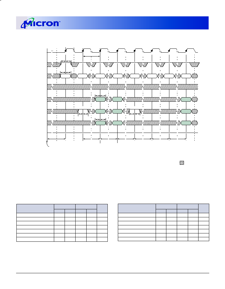
40
128Mb: x16, x32 Mobile SDRAM
Micron Technology, Inc., reserves the right to change products or specifications without notice.
MobileY95W_3V_F.p65 � Rev. F; Pub. 9/02
�2002, Micron Technology, Inc.
128Mb: x16, x32
MOBILE SDRAM
ADVANCE
INITIALIZE AND LOAD MODE REGISTER
1,2
*CAS latency indicated in parentheses.
-8
-10
SYMBOL*
MIN
MAX
MIN
MAX
UNITS
t
CKH
1
1
ns
t
CKS
2.5
2.5
ns
t
CMH
1
1
ns
t
CMS
2.5
2.5
ns
t
MRD
3
2
2
t
CK
t
RFC
80
100
ns
t
RP
20
20
ns
TIMING PARAMETERS
-8
-10
SYMBOL*
MIN
MAX
MIN
MAX
UNITS
t
AH
1
1
ns
t
AS
2.5
2.5
ns
t
CH
3
3
ns
t
CL
3
3
ns
t
CK (3)
8
10
ns
t
CK (2)
10
12
ns
t
CK (1)
20
25
ns
CKE
BA0, BA1
Load Extended
Mode Register
Load Mode
Register
t
CKS
Power-up:
V
DD
and
CLK stable
T = 100�s
t
CKH
(
)
(
)
(
)
(
)
(
)
(
)
(
)
(
)
(
)
(
)
(
)
(
)
(
)
(
)
(
)
(
)
(
)
(
)
(
)
(
)
(
)
(
)
(
)
(
)
(
)
(
)
(
)
(
)
(
)
(
)
(
)
(
)
(
)
(
)
(
)
(
)
(
)
(
)
(
)
(
)
(
)
(
)
(
)
(
)
(
)
(
)
(
)
(
)
(
)
(
)
(
)
(
)
(
)
(
)
(
)
(
)
DQML, DQMU
(
)
(
)
(
)
(
)
(
)
(
)
(
)
(
)
DQ
High-Z
A0-A9, A11
RA
A10
RA
ALL BANKS
CLK
t
CK
COMMAND
5
LMR4
NOP
PRE3
LMR4
AR4
AR4
ACT4
t
CMS
t
CMH
BA0 = L,
BA1 = H
tAS tAH
t
AS
t
AH
BA0 = L,
BA1 = L
(
)
(
)
(
)
(
)
CODE CODE
tAS tAH
CODE CODE
(
)
(
)
(
)
(
)
PRE
ALL BANKS
tAS tAH
NOTE:
1. The two AUTO REFRESH commands at T9 and T19 may be applied before either LOAD MODE REGISTER (LMR) command.
2. PRE = PRECHARGE command, LMR = LOAD MODE REGISTER command, AR = AUTO REFRESH command, ACT = ACTIVE command, RA = Row Address,
BA = Bank Address
3. Optional refresh command.
4. The Load Mode Register for both MR/EMR and 2 Auto Refresh commands can be in any order. However, all must occur prior to an Active command.
5. Device timing is -10 with 100 MHz clock.
(
)
(
)
(
)
(
)
T0
T1
T3
T5
T7
T9
T19
T29
DON'T CARE
BA
(
)
(
)
(
)
(
)
(
)
(
)
(
)
(
)
(
)
(
)
(
)
(
)
(
)
(
)
(
)
(
)
(
)
(
)
(
)
(
)
(
)
(
)
(
)
(
)
(
)
(
)
(
)
(
)
(
)
(
)
(
)
(
)
(
)
(
)
(
)
(
)
(
)
(
)
(
)
(
)
(
)
(
)
(
)
(
)
(
)
(
)
(
)
(
)
(
)
(
)
(
)
(
)
(
)
(
)
(
)
(
)
(
)
(
)
(
)
(
)
(
)
(
)
(
)
(
)
(
)
(
)
(
)
(
)
(
)
(
)
(
)
(
)
(
)
(
)
(
)
(
)
(
)
(
)
(
)
(
)
(
)
(
)
(
)
(
)
(
)
(
)
(
)
(
)
(
)
(
)
(
)
(
)
(
)
(
)
(
)
(
)
(
)
(
)
(
)
(
)
(
)
(
)
(
)
(
)
(
)
(
)
t
RP
t
MRD
t
MRD
t
RP
t
RFC
t
RFC
(
)
(
)
(
)
(
)
(
)
(
)
(
)
(
)
(
)
(
)
(
)
(
)
(
)
(
)
(
)
(
)
(
)
(
)
(
)
(
)
(
)
(
)
(
)
(
)
(
)
(
)
(
)
(
)
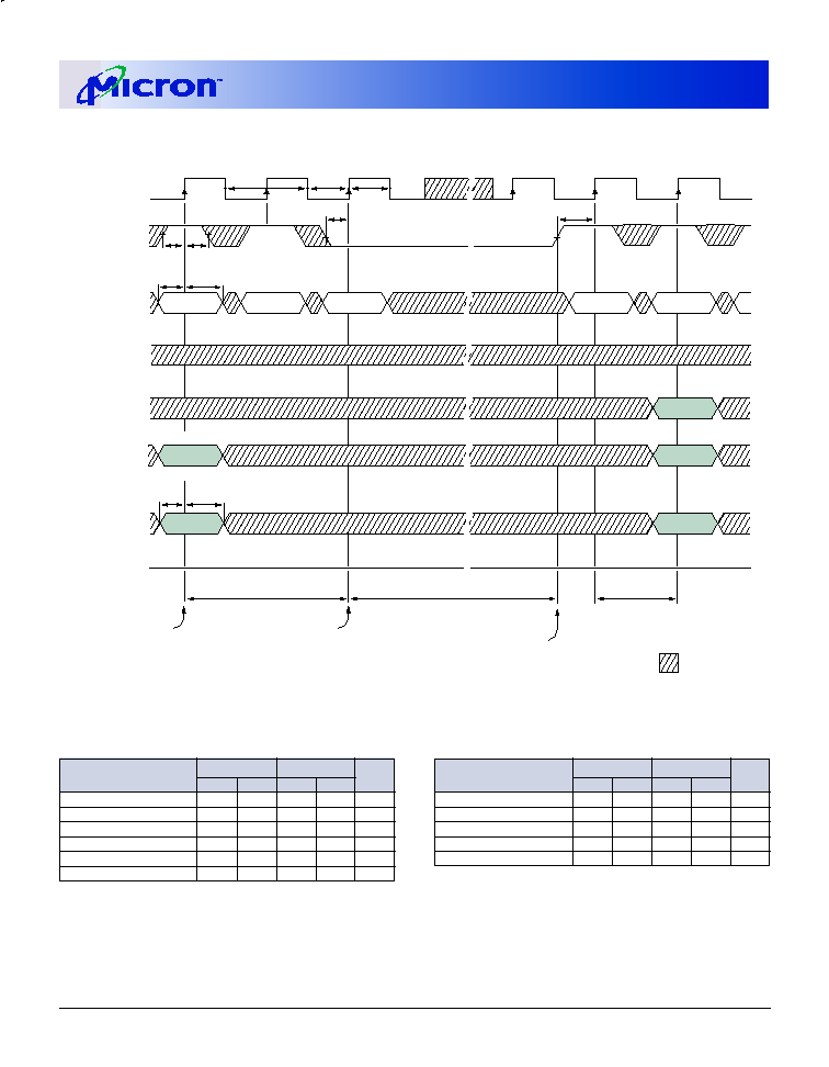
41
128Mb: x16, x32 Mobile SDRAM
Micron Technology, Inc., reserves the right to change products or specifications without notice.
MobileY95W_3V_F.p65 � Rev. F; Pub. 9/02
�2002, Micron Technology, Inc.
128Mb: x16, x32
MOBILE SDRAM
ADVANCE
NOTE: 1. Violating refresh requirements during power-down may result in a loss of data.
POWER-DOWN MODE
1
tCH
tCL
tCK
Two clock cycles
CKE
CLK
DQ
All banks idle, enter
power-down mode
Precharge all
active banks
Input buffers gated off while in
power-down mode
Exit power-down mode
(
)
(
)
(
)
(
)
DON'T CARE
tCKS
tCKS
COMMAND
tCMH
tCMS
PRECHARGE
NOP
NOP
ACTIVE
NOP
(
)
(
)
(
)
(
)
All banks idle
BA0, BA1
BANK
BANK(S)
(
)
(
)
(
)
(
)
High-Z
tAH
tAS
tCKH
tCKS
DQML, DQMU
(
)
(
)
(
)
(
)
(
)
(
)
(
)
(
)
A0-A9, A11
ROW
(
)
(
)
(
)
(
)
ALL BANKS
SINGLE BANK
A10
ROW
(
)
(
)
(
)
(
)
T0
T1
T2
Tn + 1
Tn + 2
*CAS latency indicated in parentheses.
-8
-10
SYMBOL*
MIN
MAX
MIN
MAX
UNITS
t
CK (1)
20
25
ns
t
CKH
1
1
ns
t
CKS
2.5
2.5
ns
t
CMH
1
1
ns
t
CMS
2.5
2.5
ns
TIMING PARAMETERS
-8
-10
SYMBOL*
MIN
MAX
MIN
MAX
UNITS
t
AH
1
1
ns
t
AS
2.5
2.5
ns
t
CH
3
3
ns
t
CL
3
3
ns
t
CK (3)
8
10
ns
t
CK (2)
10
12
ns
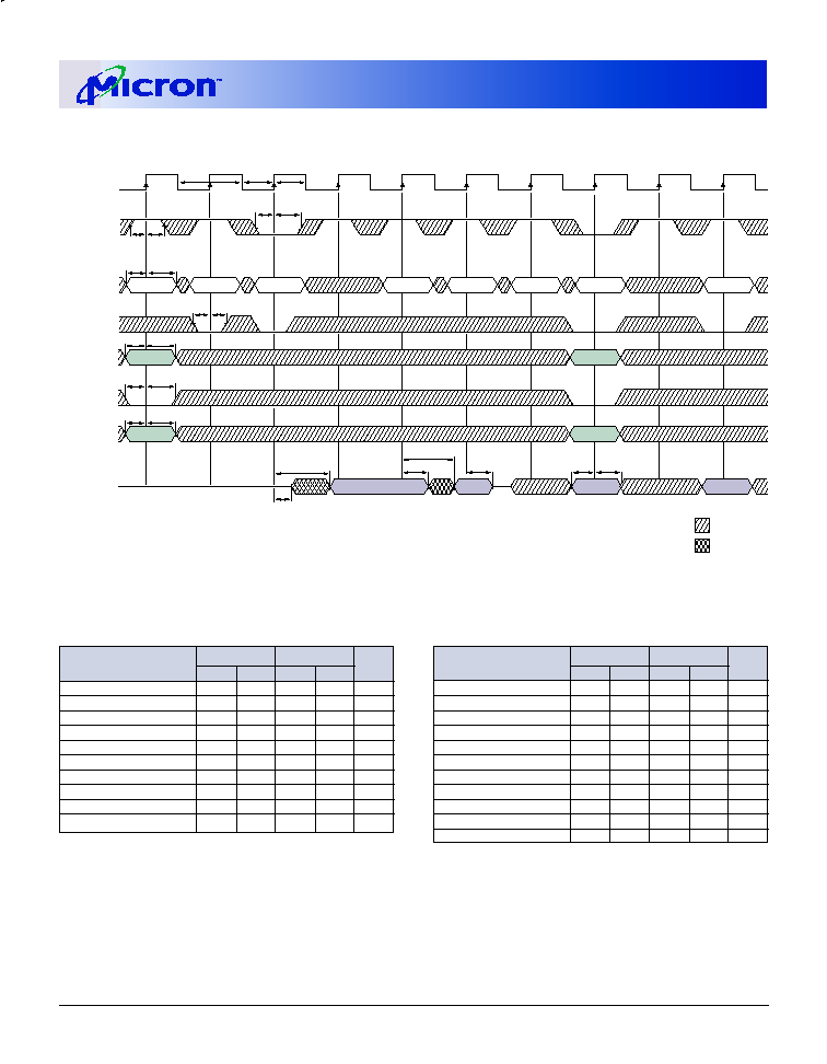
42
128Mb: x16, x32 Mobile SDRAM
Micron Technology, Inc., reserves the right to change products or specifications without notice.
MobileY95W_3V_F.p65 � Rev. F; Pub. 9/02
�2002, Micron Technology, Inc.
128Mb: x16, x32
MOBILE SDRAM
ADVANCE
CLOCK SUSPEND MODE
1
tCH
tCL
tCK
tAC
tLZ
DQMU, DQML
CLK
A0-A9, A11
DQ
BA0, BA1
A10
tOH
D
OUT
m
tAH
tAS
tAH
tAS
tAH
tAS
BANK
tDH
D
OUT
e
tAC
tHZ
D
OUT
m + 1
COMMAND
tCMH
tCMS
NOP
NOP
NOP
NOP
NOP
READ
WRITE
DON'T CARE
UNDEFINED
CKE
tCKS tCKH
BANK
COLUMN m
tDS
D
OUT
e + 1
NOP
tCKH
tCKS
tCMH
tCMS
2
COLUMN e2
T0
T1
T2
T3
T4
T5
T6
T7
T8
T9
NOTE: 1. For this example, the burst length = 2, the CAS latency = 3, and auto precharge is disabled.
2. x16: A9 and A11 = "Don't Care"
x32: A8, A9 and A11 = "Don't Care"
*CAS latency indicated in parentheses.
-8
-10
SYMBOL*
MIN
MAX
MIN
MAX
UNITS
t
CKH
1
1
ns
t
CKS
2.5
2.5
ns
t
CMH
1
1
ns
t
CMS
2.5
2.5
ns
t
DH
1
1
ns
t
DS
2.5
2.5
ns
t
HZ (3)
7
7
ns
t
HZ (2)
8
8
ns
t
HZ (1)
19
22
ns
t
LZ
1
1
ns
t
OH
2.5
2.5
ns
TIMING PARAMETERS
-8
-10
SYMBOL*
MIN
MAX
MIN
MAX
UNITS
t
AC (3)
7
7
ns
t
AC (2)
8
8
ns
t
AC (1)
19
22
ns
t
AH
1
1
ns
t
AS
2.5
2.5
ns
t
CH
3
3
ns
t
CL
3
3
ns
t
CK (3)
8
10
ns
t
CK (2)
10
12
ns
t
CK (1)
20
25
ns
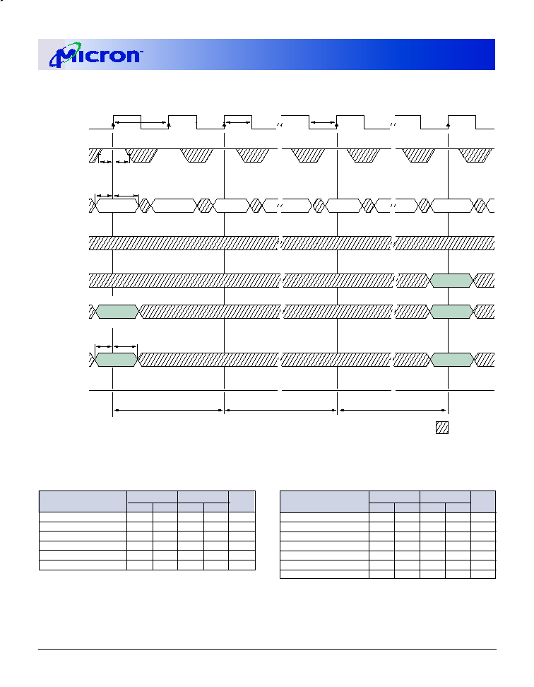
43
128Mb: x16, x32 Mobile SDRAM
Micron Technology, Inc., reserves the right to change products or specifications without notice.
MobileY95W_3V_F.p65 � Rev. F; Pub. 9/02
�2002, Micron Technology, Inc.
128Mb: x16, x32
MOBILE SDRAM
ADVANCE
AUTO REFRESH MODE
tCH
tCL
tCK
CKE
CLK
DQ
tRFC
1
(
)
(
)
(
)
(
)
(
)
(
)
tRP
(
)
(
)
(
)
(
)
(
)
(
)
(
)
(
)
COMMAND
tCMH
tCMS
NOP
NOP
(
)
(
)
(
)
(
)
BANK
ACTIVE
AUTO
REFRESH
(
)
(
)
(
)
(
)
NOP
NOP
PRECHARGE
Precharge all
active banks
AUTO
REFRESH
tRFC
1
High-Z
BA0, BA1
BANK(S)
(
)
(
)
(
)
(
)
(
)
(
)
(
)
(
)
tAH
tAS
tCKH
tCKS
(
)
(
)
NOP
(
)
(
)
(
)
(
)
(
)
(
)
(
)
(
)
DQMU, DQML
A0-A9, A11
ROW
(
)
(
)
(
)
(
)
ALL BANKS
SINGLE BANK
A10
ROW
(
)
(
)
(
)
(
)
(
)
(
)
(
)
(
)
(
)
(
)
(
)
(
)
(
)
(
)
(
)
(
)
T0
T1
T2
Tn + 1
To + 1
DON'T CARE
*CAS latency indicated in parentheses.
-8
-10
SYMBOL*
MIN
MAX
MIN
MAX
UNITS
t
CK (1)
20
25
ns
t
CKH
1
1
ns
t
CKS
2.5
2.5
ns
t
CMH
1
1
ns
t
CMS
2.5
2.5
ns
t
RFC
80
100
ns
t
RP
20
20
ns
TIMING PARAMETERS
-8
-10
SYMBOL*
MIN
MAX
MIN
MAX
UNITS
t
AH
1
1
ns
t
AS
2.5
2.5
ns
t
CH
3
3
ns
t
CL
3
3
ns
t
CK (3)
8
10
ns
t
CK (2)
10
12
ns
NOTE: 1. Each AUTO REFRESH command performs a refresh cycle. Back-to-back commands are not required.
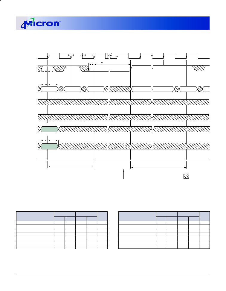
44
128Mb: x16, x32 Mobile SDRAM
Micron Technology, Inc., reserves the right to change products or specifications without notice.
MobileY95W_3V_F.p65 � Rev. F; Pub. 9/02
�2002, Micron Technology, Inc.
128Mb: x16, x32
MOBILE SDRAM
ADVANCE
SELF REFRESH MODE
*CAS latency indicated in parentheses.
-8
-10
SYMBOL*
MIN
MAX
MIN
MAX
UNITS
t
CKH
1
1
ns
t
CKS
2.5
2.5
ns
t
CMH
1
1
ns
t
CMS
2.5
2.5
ns
t
RAS
48
120,000
50
120,000
ns
t
RP
20
20
ns
t
XSR
80
100
ns
TIMING PARAMETERS
-8
-10
SYMBOL*
MIN
MAX
MIN
MAX
UNITS
t
AH
1
1
ns
t
AS
2.5
2.5
ns
t
CH
3
3
ns
t
CL
3
3
ns
t
CK (3)
8
10
ns
t
CK (2)
10
12
ns
t
CK (1)
20
25
ns
DON'T CARE
tCH
tCL
tCK
tRP
CKE
CLK
DQ
Enter self refresh mode
Precharge all
active banks
tXSR
CLK stable prior to exiting
self refresh mode
Exit self refresh mode
(Restart refresh time base)
(
)
(
)
(
)
(
)
(
)
(
)
(
)
(
)
(
)
(
)
(
)
(
)
(
)
(
)
COMMAND
tCMH
tCMS
AUTO
REFRESH
PRECHARGE
NOP
NOP
(
)
(
)
(
)
(
)
(
)
(
)
(
)
(
)
BA0, BA1
BANK(S)
High-Z
tCKS
AH
AS
AUTO
REFRESH
> tRAS
(
)
(
)
(
)
(
)
(
)
(
)
(
)
(
)
tCKH
tCKS
DQMU, DQML
(
)
(
)
(
)
(
)
(
)
(
)
(
)
(
)
t
t
A0-A9, A11
(
)
(
)
(
)
(
)
ALL BANKS
SINGLE BANK
A10
(
)
(
)
(
)
(
)
(
)
(
)
(
)
(
)
(
)
(
)
(
)
(
)
T0
T1
T2
Tn + 1
To + 1
To + 2
(
)
(
)
(
)
(
)
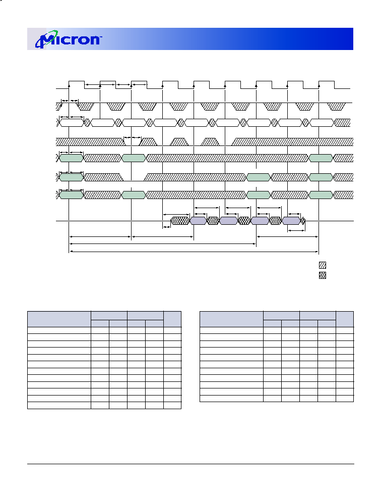
45
128Mb: x16, x32 Mobile SDRAM
Micron Technology, Inc., reserves the right to change products or specifications without notice.
MobileY95W_3V_F.p65 � Rev. F; Pub. 9/02
�2002, Micron Technology, Inc.
128Mb: x16, x32
MOBILE SDRAM
ADVANCE
READ � WITHOUT AUTO PRECHARGE
1
ALL BANKS
tCH
tCL
tCK
tAC
tLZ
tRP
tRAS
tRCD
CAS Latency
tRC
tOH
D
OUT
m
tCMH
tCMS
tAH
tAS
tAH
tAS
tAH
tAS
ROW
ROW
BANK
BANK(S)
BANK
ROW
ROW
BANK
tHZ
tOH
D
OUT
m+3
tAC
tOH
tAC
tOH
tAC
D
OUT
m+2
D
OUT
m+1
tCMH
tCMS
PRECHARGE
NOP
NOP
NOP
ACTIVE
NOP
READ
NOP
ACTIVE
DISABLE AUTO PRECHARGE
SINGLE BANKS
DON'T CARE
UNDEFINED
COLUMN m
2
tCKH
tCKS
T0
T1
T2
T3
T4
T5
T6
T7
T8
DQMU, DQML
CKE
CLK
A0-A9, A11
DQ
BA0, BA1
A10
COMMAND
TIMING PARAMETERS
-8
-10
SYMBOL*
MIN
MAX
MIN
MAX
UNITS
t
AC (3)
7
7
ns
t
AC (2)
8
8
ns
t
AC (1)
19
22
ns
t
AH
1
1
ns
t
AS
2.5
2.5
ns
t
CH
3
3
ns
t
CL
3
3
ns
t
CK (3)
8
10
ns
t
CK (2)
10
12
ns
t
CK (1)
20
25
ns
t
CKH
1
1
ns
t
CKS
2.5
2.5
ns
t
CMH
1
1
ns
t
CMS
2.5
2.5
ns
t
HZ (3)
7
7
ns
t
HZ (2)
8
8
ns
t
HZ (1)
19
22
ns
t
LZ
1
1
ns
t
OH
2.5
2.5
ns
t
RAS
48
120,000
50
120,000
ns
t
RC
80
100
ns
t
RCD
20
20
ns
t
RP
20
20
ns
*CAS latency indicated in parentheses.
NOTE: 1. For this example, the burst length = 4, the CAS latency = 2, and the READ burst is followed by a "manual"
PRECHARGE.
2. x16: A9 and A11 = "Don't Care"
x32: A8, A9,and A11 = "Don't Care"
-8
-10
SYMBOL*
MIN
MAX
MIN
MAX
UNITS
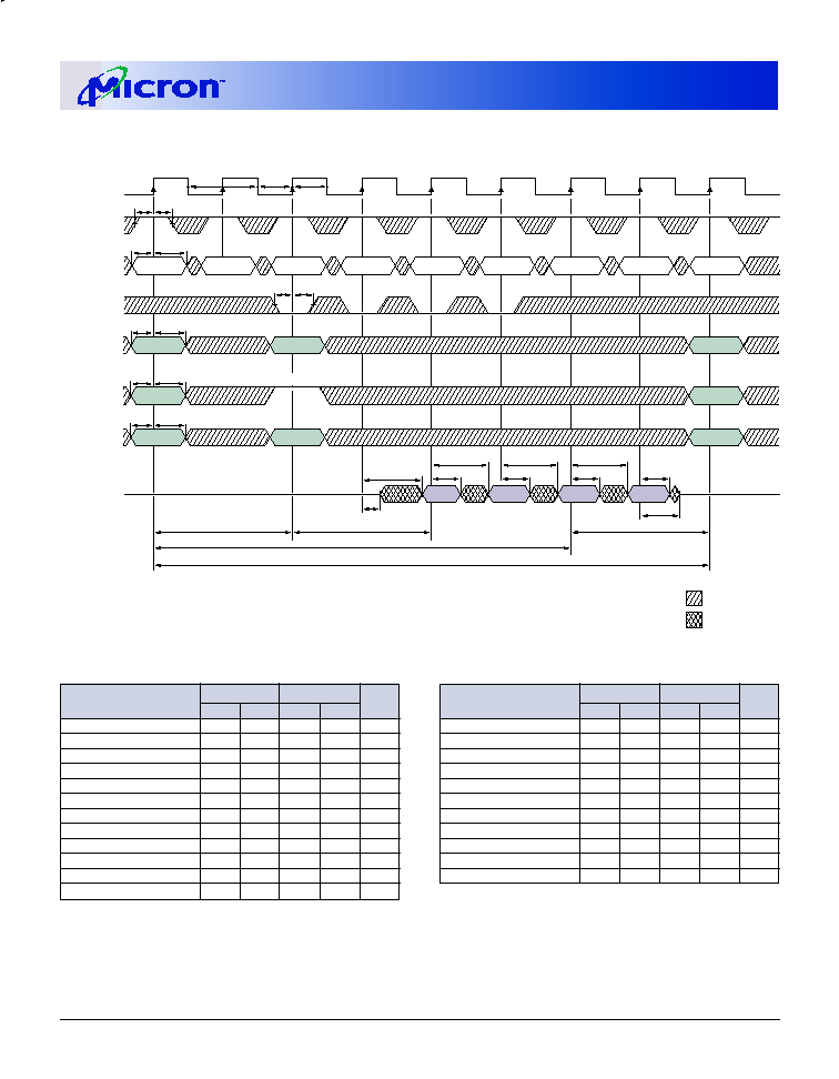
46
128Mb: x16, x32 Mobile SDRAM
Micron Technology, Inc., reserves the right to change products or specifications without notice.
MobileY95W_3V_F.p65 � Rev. F; Pub. 9/02
�2002, Micron Technology, Inc.
128Mb: x16, x32
MOBILE SDRAM
ADVANCE
READ � WITH AUTO PRECHARGE
1
ENABLE AUTO PRECHARGE
tCH
tCL
tCK
tAC
tLZ
tRP
tRAS
tRCD
CAS Latency
tRC
DQMU, DQML
CKE
CLK
A0-A9, A11
DQ
BA0, BA1
A10
tOH
D
OUT
m
tCMH
tCMS
tAH
tAS
tAH
tAS
tAH
tAS
ROW
ROW
BANK
BANK
ROW
ROW
BANK
DON'T CARE
UNDEFINED
tHZ
tOH
D
OUT
m + 3
tAC
tOH
tAC
tOH
tAC
D
OUT
m + 2
D
OUT
m + 1
COMMAND
tCMH
tCMS
NOP
NOP
NOP
ACTIVE
NOP
READ
NOP
ACTIVE
NOP
tCKH
tCKS
COLUMN m 2
T0
T1
T2
T4
T3
T5
T6
T7
T8
NOTE: 1. For this example, the burst length = 4, and the CAS latency = 2.
2. x16: A9 and A11 = "Don't Care"
x32: A8, A9,and A11 = "Don't Care"
*CAS latency indicated in parentheses.
-8
-10
SYMBOL*
MIN
MAX
MIN
MAX
UNITS
t
CMH
1
1
ns
t
CMS
2.5
2.5
ns
t
HZ (3)
7
7
ns
t
HZ (2)
8
8
ns
t
HZ (1)
19
22
ns
t
LZ
1
1
ns
t
OH
2.5
2.5
ns
t
RAS
48
120,000
50
120,000
ns
t
RC
80
70
ns
t
RCD
20
20
ns
t
RP
20
20
ns
TIMING PARAMETERS
-8
-10
SYMBOL*
MIN
MAX
MIN
MAX
UNITS
t
AC (3)
7
7
ns
t
AC (2)
8
8
ns
t
AC (1)
19
22
ns
t
AH
1
1
ns
t
AS
2.5
2.5
ns
t
CH
3
3
ns
t
CL
3
3
ns
t
CK (3)
8
10
ns
t
CK (2)
10
12
ns
t
CK (1)
20
25
ns
t
CKH
1
1
ns
t
CKS
2.5
2.5
ns
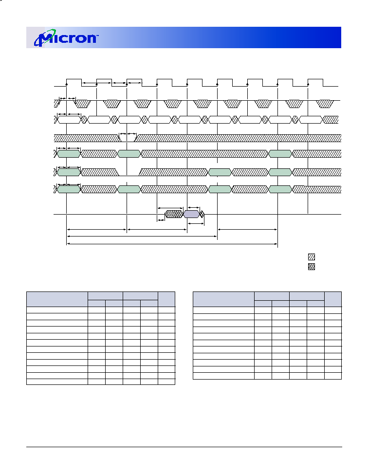
47
128Mb: x16, x32 Mobile SDRAM
Micron Technology, Inc., reserves the right to change products or specifications without notice.
MobileY95W_3V_F.p65 � Rev. F; Pub. 9/02
�2002, Micron Technology, Inc.
128Mb: x16, x32
MOBILE SDRAM
ADVANCE
NOTE: 1. For this example, the burst length = 1, the CAS latency = 2, and the READ burst is followed by a "manual"
PRECHARGE.
2. x16: A9 and A11 = "Don't Care"
x32: A8, A9,and A11 = "Don't Care"
3. PRECHARGE command not allowed or
t
RAS would be violated.
*CAS latency indicated in parentheses.
-8
-10
SYMBOL*
MIN
MAX
MIN
MAX
UNITS
t
CMH
1
1
ns
t
CMS
2.5
2.5
ns
t
HZ (3)
7
7
ns
t
HZ (2)
8
8
ns
t
HZ (1)
19
22
ns
t
LZ
1
1
ns
t
OH
2.5
2.5
ns
t
RAS
48
120,000
50
120,000
ns
t
RC
80
100
ns
t
RCD
20
20
ns
t
RP
20
20
ns
TIMING PARAMETERS
-8
-10
SYMBOL*
MIN
MAX
MIN
MAX
UNITS
t
AC (3)
7
7
ns
t
AC (2)
8
8
ns
t
AC (1)
19
22
ns
t
AH
1
1
ns
t
AS
2.5
2.5
ns
t
CH
3
3
ns
t
CL
3
3
ns
t
CK (3)
8
10
ns
t
CK (2)
10
12
ns
t
CK (1)
20
25
ns
t
CKH
1
1
ns
t
CKS
2.5
2.5
ns
SINGLE READ � WITHOUT AUTO PRECHARGE
1
ALL BANKS
tCH
tCL
tCK
tAC
tLZ
tRP
tRAS
tRCD
CAS Latency
tRC
tOH
D
OUT
m
tCMH
tCMS
tAH
tAS
tAH
tAS
tAH
tAS
ROW
ROW
BANK
BANK(S)
BANK
ROW
ROW
BANK
tHZ
tCMH
tCMS
NOP
NOP
NOP
PRECHARGE
ACTIVE
NOP
READ
ACTIVE
NOP
DISABLE AUTO PRECHARGE
SINGLE BANKS
DON'T CARE
UNDEFINED
COLUMN m
2
tCKH
tCKS
T0
T1
T2
T3
T4
T5
T6
T7
T8
DQMU, DQML
CKE
CLK
A0-A9, A11
DQ
BA0, BA1
A10
COMMAND
3
3
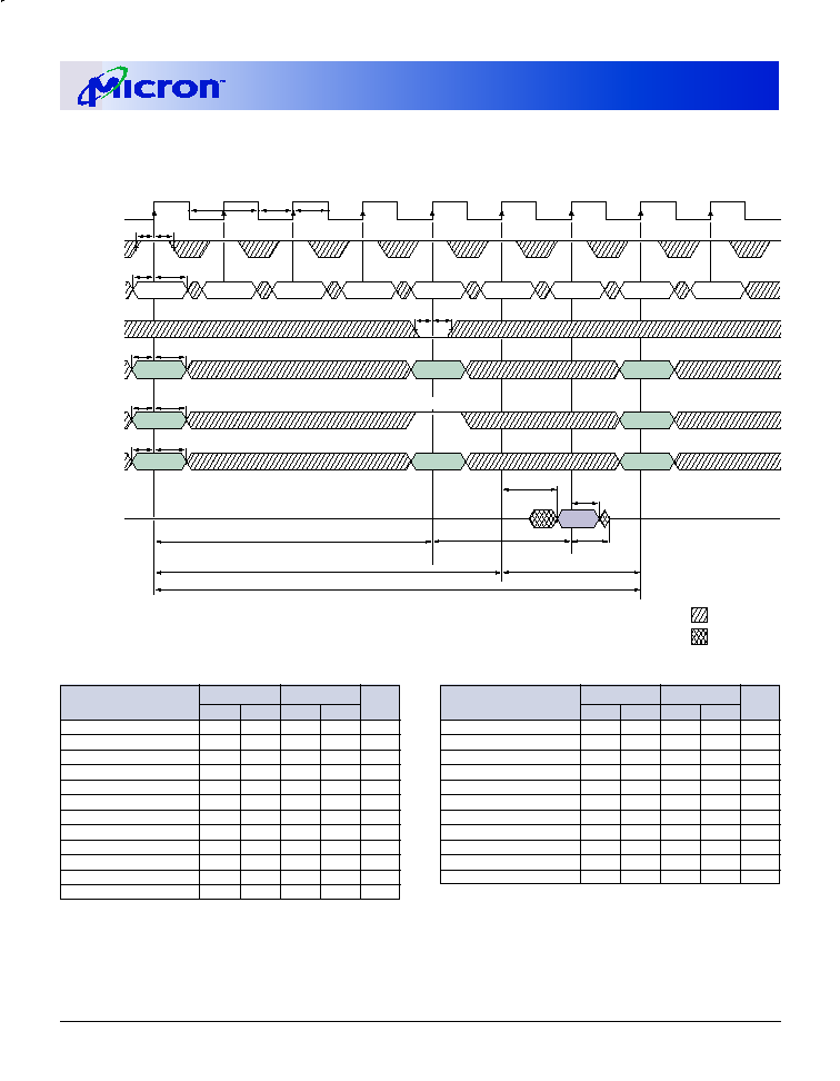
48
128Mb: x16, x32 Mobile SDRAM
Micron Technology, Inc., reserves the right to change products or specifications without notice.
MobileY95W_3V_F.p65 � Rev. F; Pub. 9/02
�2002, Micron Technology, Inc.
128Mb: x16, x32
MOBILE SDRAM
ADVANCE
ENABLE AUTO PRECHARGE
tCH
tCL
tCK
tRP
tRAS
tRCD
CAS Latency
tRC
DQMU, DQML
CKE
CLK
A0-A9, A11
DQ
BA0, BA1
A10
tCMH
tCMS
tAH
tAS
tAH
tAS
tAH
tAS
ROW
ROW
BANK
BANK
ROW
ROW
BANK
DON'T CARE
UNDEFINED
tHZ
t OH
D
OUT
m
tAC
COMMAND
tCMH
tCMS
NOP3
READ
ACTIVE
NOP
NOP3
ACTIVE
NOP
tCKH
tCKS
COLUMN m2
T0
T1
T2
T4
T3
T5
T6
T7
T8
NOP
NOP
NOTE: 1. For this example, the burst length = 1, and the CAS latency = 2.
2. x16: A9 and A11 = "Don't Care"
x32: A8, A9,and A11 = "Don't Care"
3. READ command not allowed else
t
RAS would be violated.
*CAS latency indicated in parentheses.
-8
-10
SYMBOL*
MIN
MAX
MIN
MAX
UNITS
t
CMH
1
1
ns
t
CMS
2.5
2.5
ns
t
HZ (3)
7
7
ns
t
HZ (2)
8
8
ns
t
HZ (1)
19
22
ns
t
LZ
1
1
ns
t
OH
2.5
2.5
ns
t
RAS
48
120,000
50
120,000
ns
t
RC
80
100
ns
t
RCD
20
20
ns
t
RP
20
20
ns
TIMING PARAMETERS
-8
-10
SYMBOL*
MIN
MAX
MIN
MAX
UNITS
t
AC (3)
7
7
ns
t
AC (2)
8
8
ns
t
AC (1)
19
22
ns
t
AH
1
1
ns
t
AS
2.5
2.5
ns
t
CH
3
3
ns
t
CL
3
3
ns
t
CK (3)
8
10
ns
t
CK (2)
10
12
ns
t
CK (1)
20
25
ns
t
CKH
1
1
ns
t
CKS
2.5
2.5
ns
SINGLE READ � WITH AUTO PRECHARGE
1
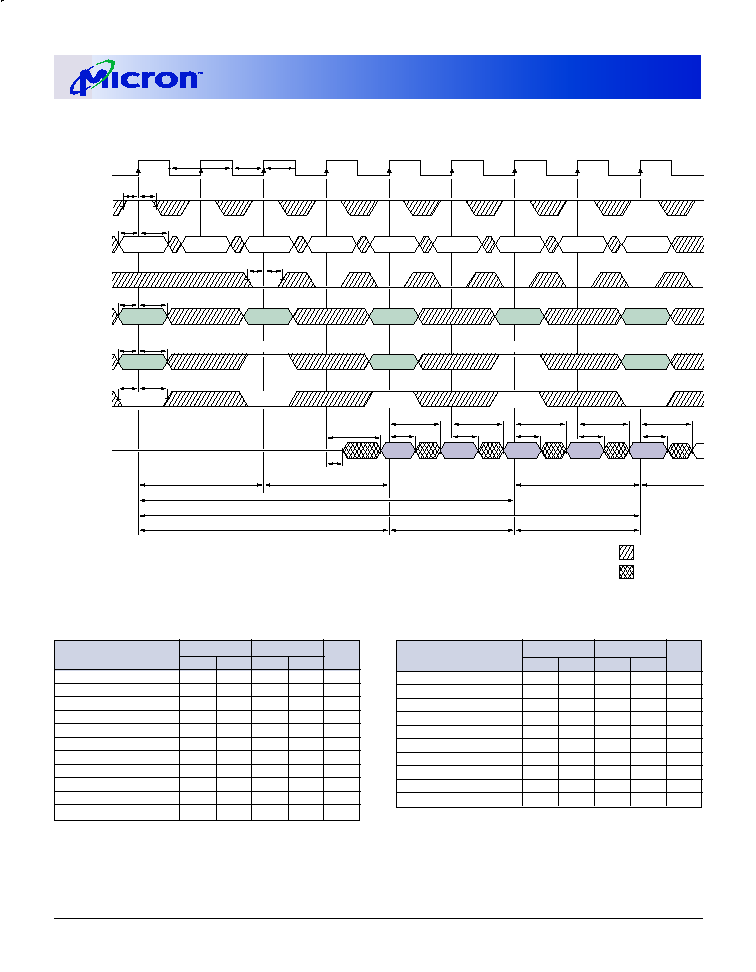
49
128Mb: x16, x32 Mobile SDRAM
Micron Technology, Inc., reserves the right to change products or specifications without notice.
MobileY95W_3V_F.p65 � Rev. F; Pub. 9/02
�2002, Micron Technology, Inc.
128Mb: x16, x32
MOBILE SDRAM
ADVANCE
ALTERNATING BANK READ ACCESSES
1
ENABLE AUTO PRECHARGE
tCH
tCL
tCK
tAC
tLZ
DQMU, DQML
CLK
A0-A9, A11
DQ
BA0, BA1
A10
tOH
D
OUT
m
tCMH
tCMS
tAH
tAS
tAH
tAS
tAH
tAS
ROW
ROW
ROW
ROW
DON'T CARE
UNDEFINED
tOH
D
OUT
m + 3
tAC
tOH
tAC
tOH
tAC
D
OUT
m + 2
D
OUT
m + 1
COMMAND
tCMH
tCMS
NOP
NOP
ACTIVE
NOP
READ
NOP
ACTIVE
tOH
D
OUT
b
tAC
tAC
READ
ENABLE AUTO PRECHARGE
ROW
ACTIVE
ROW
BANK 0
BANK 0
BANK 3
BANK 3
BANK 0
CKE
tCKH
tCKS
COLUMN m 2
COLUMN b 2
T0
T1
T2
T4
T3
T5
T6
T7
T8
tRP - BANK 0
tRAS - BANK 0
tRCD - BANK 0
tRCD - BANK 0
CAS Latency - BANK 0
tRCD - BANK 3
CAS Latency - BANK 3
t
t
RC - BANK 0
RRD
NOTE: 1. For this example, the burst length = 4, and the CAS latency = 2.
2. x16: A9 and A11 = "Don't Care"
x32: A8, A9,and A11 = "Don't Care"
*CAS latency indicated in parentheses.
-8
-10
SYMBOL*
MIN
MAX
MIN
MAX
UNITS
t
CKS
2.5
2.5
ns
t
CMH
1
1
ns
t
CMS
2.5
2.5
ns
t
LZ
1
1
ns
t
OH
2.5
2.5
ns
t
RAS
48
120,000
50
120,000
ns
t
RC
80
100
ns
t
RCD
20
20
ns
t
RP
20
20
ns
t
RRD
20
20
ns
TIMING PARAMETERS
-8
-10
SYMBOL*
MIN
MAX
MIN
MAX
UNITS
t
AC (3)
7
7
ns
t
AC (2)
8
8
ns
t
AC (1)
19
22
ns
t
AH
1
1
ns
t
AS
2.5
2.5
ns
t
CH
3
3
ns
t
CL
3
3
ns
t
CK (3)
8
10
ns
t
CK (2)
10
12
ns
t
CK (1)
20
25
ns
t
CKH
1
1
ns
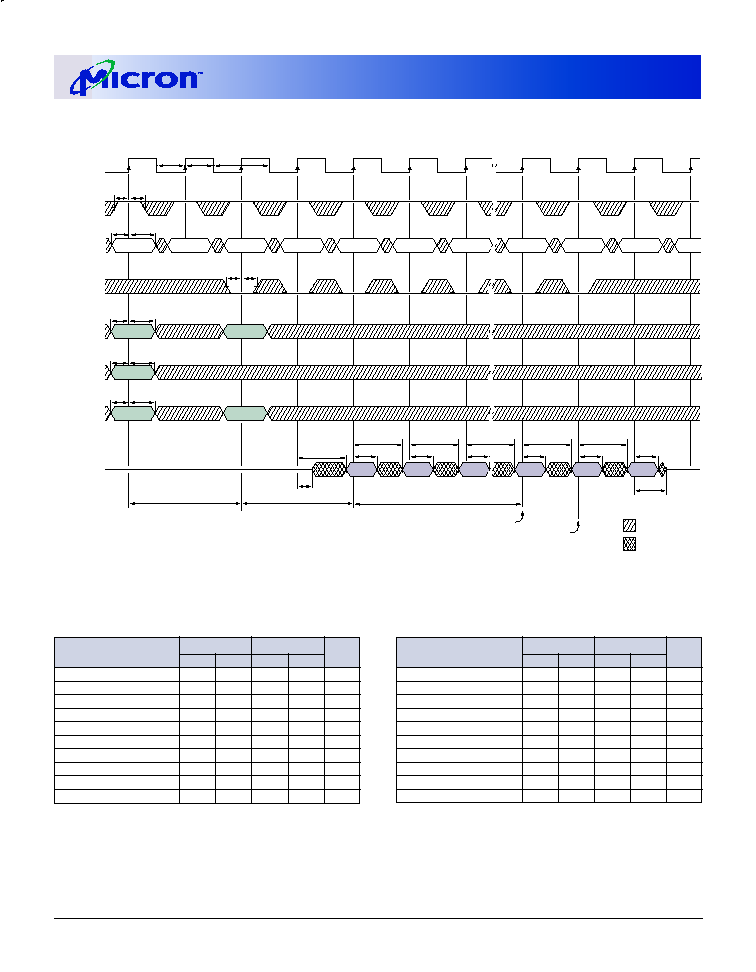
50
128Mb: x16, x32 Mobile SDRAM
Micron Technology, Inc., reserves the right to change products or specifications without notice.
MobileY95W_3V_F.p65 � Rev. F; Pub. 9/02
�2002, Micron Technology, Inc.
128Mb: x16, x32
MOBILE SDRAM
ADVANCE
READ � FULL-PAGE BURST
1
tCH
tCL
tCK
tAC
tLZ
tRCD
CAS Latency
DQMU, DQML
CKE
CLK
A0-A9, A11
DQ
BA0, BA1
A10
tOH
D
OUT
m
tCMH
tCMS
tAH
tAS
tAH
tAS
tAC
tOH
D
OUT
m+1
ROW
ROW
tHZ
tAC
tOH
D
OUT
m+1
tAC
tOH
D
OUT
m+2
tAC
tOH
D
OUT
m-1
tAC
tOH
D
OUT
m
Full-page burst does not self-terminate.
Can use BURST TERMINATE command.
(
)
(
)
(
)
(
)
(
)
(
)
(
)
(
)
(
)
(
)
(
)
(
)
(
)
(
)
Full page completed
512 (x16) locations within same row
DON'T CARE
UNDEFINED
COMMAND
tCMH
tCMS
NOP
NOP
NOP
ACTIVE
NOP
READ
NOP
BURST TERM
NOP
NOP
(
)
(
)
(
)
(
)
NOP
(
)
(
)
(
)
(
)
tAH
tAS
BANK
(
)
(
)
(
)
(
)
BANK
tCKH
tCKS
(
)
(
)
(
)
(
)
(
)
(
)
(
)
(
)
COLUMN m 2
3
T0
T1
T2
T4
T3
T5
T6
Tn + 1
Tn + 2
Tn + 3
Tn + 4
NOTE: 1. For this example, the CAS latency = 2.
2. x16: A9 and A11 = "Don't Care"
x32: A8, A9,and A11 = "Don't Care"
3. Page left open; no
t
RP.
*CAS latency indicated in parentheses.
-8
-10
SYMBOL*
MIN
MAX
MIN
MAX
UNITS
t
CKH
1
1
ns
t
CKS
2.5
2.5
ns
t
CMH
1
1
ns
t
CMS
2.5
2.5
ns
t
HZ (3)
7
7
ns
t
HZ (2)
8
8
ns
t
HZ (1)
19
22
ns
t
LZ
1
1
ns
t
OH
2.5
2.5
ns
t
RCD
20
20
ns
TIMING PARAMETERS
-8
-10
SYMBOL*
MIN
MAX
MIN
MAX
UNITS
t
AC (3)
7
7
ns
t
AC (2)
8
8
ns
t
AC (1)
19
22
ns
t
AH
1
1
ns
t
AS
2.5
2.5
ns
t
CH
3
3
ns
t
CL
3
3
ns
t
CK (3)
8
10
ns
t
CK (2)
10
12
ns
t
CK (1)
20
25
ns
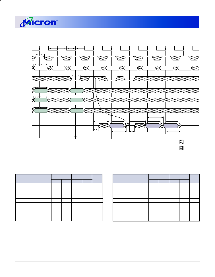
51
128Mb: x16, x32 Mobile SDRAM
Micron Technology, Inc., reserves the right to change products or specifications without notice.
MobileY95W_3V_F.p65 � Rev. F; Pub. 9/02
�2002, Micron Technology, Inc.
128Mb: x16, x32
MOBILE SDRAM
ADVANCE
READ � DQM OPERATION
1
tCH
tCL
tCK
tRCD
CAS Latency
DQMU, DQML
CKE
CLK
A0-A9, A11
DQ
BA0, BA1
A10
tCMS
ROW
BANK
ROW
BANK
tAC
LZ
D
OUT
m
tOH
D
OUT
m + 3
D
OUT
m + 2
t
tHZ
LZ
t
tCMH
COMMAND
NOP
NOP
NOP
ACTIVE
NOP
READ
NOP
NOP
NOP
tHZ
tAC
tOH
tAC
tOH
tAH
tAS
tCMS tCMH
tAH
tAS
tAH
tAS
tCKH
tCKS
ENABLE AUTO PRECHARGE
DISABLE AUTO PRECHARGE
COLUMN m 2
T0
T1
T2
T4
T3
T5
T6
T7
T8
DON'T CARE
UNDEFINED
NOTE: 1. For this example, the burst length = 4, and the CAS latency = 2.
2. x16: A9 and A11 = "Don't Care"
x32: A8, A9,and A11 = "Don't Care"
*CAS latency indicated in parentheses.
-8
-10
SYMBOL*
MIN
MAX
MIN
MAX
UNITS
t
CKH
1
1
ns
t
CKS
2.5
2.5
ns
t
CMH
1
1
ns
t
CMS
2.5
2.5
ns
t
HZ (3)
7
7
ns
t
HZ (2)
8
8
ns
t
HZ (1)
19
22
ns
t
LZ
1
1
ns
t
OH
2.5
2.5
ns
t
RCD
20
20
ns
TIMING PARAMETERS
-8
-10
SYMBOL*
MIN
MAX
MIN
MAX
UNITS
t
AC (3)
7
7
ns
t
AC (2)
8
8
ns
t
AC (1)
19
22
ns
t
AH
1
1
ns
t
AS
2.5
2.5
ns
t
CH
3
3
ns
t
CL
3
3
ns
t
CK (3)
8
10
ns
t
CK (2)
10
12
ns
t
CK (1)
20
25
ns
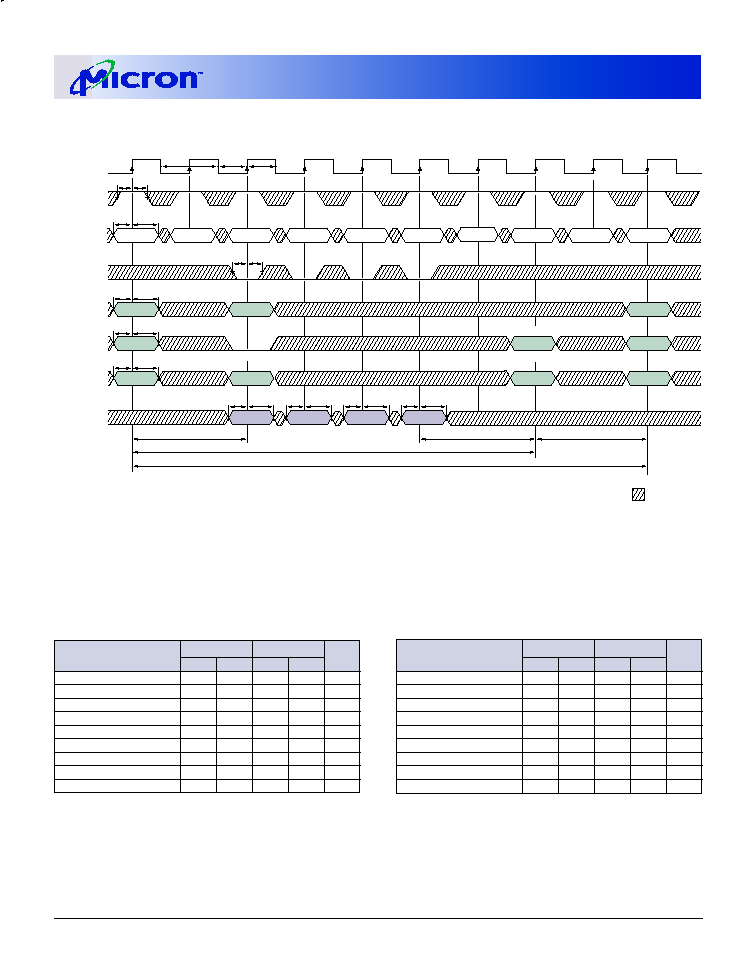
52
128Mb: x16, x32 Mobile SDRAM
Micron Technology, Inc., reserves the right to change products or specifications without notice.
MobileY95W_3V_F.p65 � Rev. F; Pub. 9/02
�2002, Micron Technology, Inc.
128Mb: x16, x32
MOBILE SDRAM
ADVANCE
WRITE � WITHOUT AUTO PRECHARGE
1
DISABLE AUTO PRECHARGE
ALL BANKS
tCH
tCL
tCK
tRP
tRAS
tRCD
tRC
DQMU, DQML
CKE
CLK
A0-A9, A11
DQ
BA0, BA1
A10
tCMH
tCMS
tAH
tAS
ROW
ROW
BANK
BANK
BANK
ROW
ROW
BANK
t WR
D
IN
m
tDH
tDS
D
IN
m + 1
D
IN
m + 2
D
IN
m + 3
COMMAND
tCMH
tCMS
NOP
NOP
NOP
ACTIVE
NOP
WRITE
NOP
PRECHARGE
ACTIVE
tAH
tAS
tAH
tAS
tDH
tDS
tDH
tDS
tDH
tDS
SINGLE BANK
tCKH
tCKS
COLUMN m 3
2
T0
T1
T2
T4
T3
T5
T6
T7
T8
DON'T CARE
T9
NOP
NOTE: 1. For this example, the burst length = 4, and the WRITE burst is followed by a "manual" PRECHARGE.
2. 15ns is required between <D
IN
m + 3> and the PRECHARGE command, regardless of frequency.
3. x16: A9 and A11 = "Don't Care"
x32: A8, A9,and A11 = "Don't Care"
*CAS latency indicated in parentheses.
-8
-10
SYMBOL*
MIN
MAX
MIN
MAX
UNITS
t
CMH
1
1
ns
t
CMS
2.5
2.5
ns
t
DH
1
1
ns
t
DS
2.5
2.5
ns
t
RAS
48
120,000
50
120,000
ns
t
RC
80
100
ns
t
RCD
20
20
ns
t
RP
20
20
ns
t
WR
15
15
ns
TIMING PARAMETERS
-8
-10
SYMBOL*
MAX
MIN
MAX
UNITS
t
AH
1
1
ns
t
AS
2.5
2.5
ns
t
CH
3
3
ns
t
CL
3
3
ns
t
CK (3)
8
10
ns
t
CK (2)
10
12
ns
t
CK (1)
20
25
ns
t
CKH
1
1
ns
t
CKS
2.5
2.5
ns
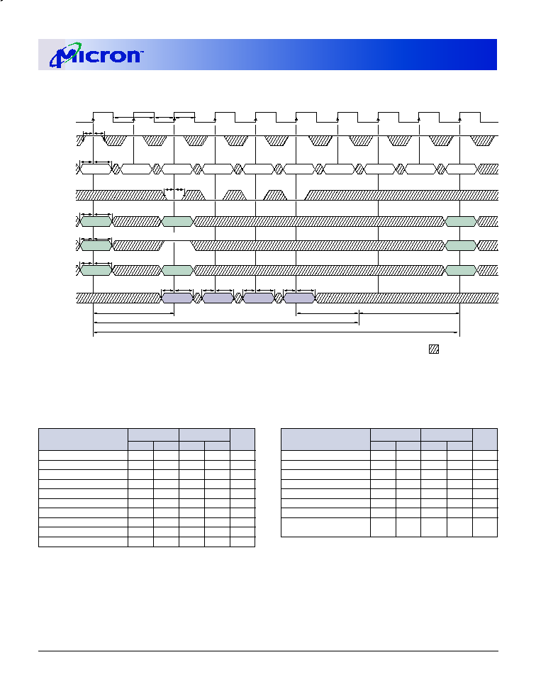
53
128Mb: x16, x32 Mobile SDRAM
Micron Technology, Inc., reserves the right to change products or specifications without notice.
MobileY95W_3V_F.p65 � Rev. F; Pub. 9/02
�2002, Micron Technology, Inc.
128Mb: x16, x32
MOBILE SDRAM
ADVANCE
WRITE � WITH AUTO PRECHARGE
1
ENABLE AUTO PRECHARGE
tCH
tCL
tCK
tRP
tRAS
tRCD
tRC
DQMU, DQML
CKE
CLK
A0-A9, A11
DQ
BA0, BA1
A10
tCMH
tCMS
tAH
tAS
ROW
ROW
BANK
BANK
ROW
ROW
BANK
tWR
D
IN
m
tDH
tDS
D
IN
m + 1
D
IN
m + 2
D
IN
m + 3
COMMAND
tCMH
tCMS
NOP
NOP
NOP
ACTIVE
NOP
WRITE
NOP
ACTIVE
tAH
tAS
tAH
tAS
tDH
tDS
tDH
tDS
tDH
tDS
tCKH
tCKS
NOP
NOP
COLUMN m 2
T0
T1
T2
T4
T3
T5
T6
T7
T8
T9
DON'T CARE
NOTE: 1. For this example, the burst length = 4.
2. x16: A9 and A11 = "Don't Care"
x32: A8, A9,and A11 = "Don't Care"
*CAS latency indicated in parentheses.
-8
-10
SYMBOL*
MIN
MAX
MIN
MAX
UNITS
t
CMS
2.5
2.5
ns
t
DH
1
1
ns
t
DS
2.5
2.5
ns
t
RAS
48
120,000
50
120,000
ns
t
RC
80
100
ns
t
RCD
20
20
ns
t
RP
20
20
ns
t
WR
1 CLK +
1 CLK +
�
7ns
5ns
TIMING PARAMETERS
-8
-10
SYMBOL*
MIN
MAX
MIN
MAX
UNITS
t
AH
1
1
ns
t
AS
2.5
2.5
ns
t
CH
3
3
ns
t
CL
3
3
ns
t
CK (3)
8
10
ns
t
CK (2)
10
12
ns
t
CK (1)
20
25
ns
t
CKH
1
1
ns
t
CKS
2.5
2.5
ns
t
CMH
1
1
ns
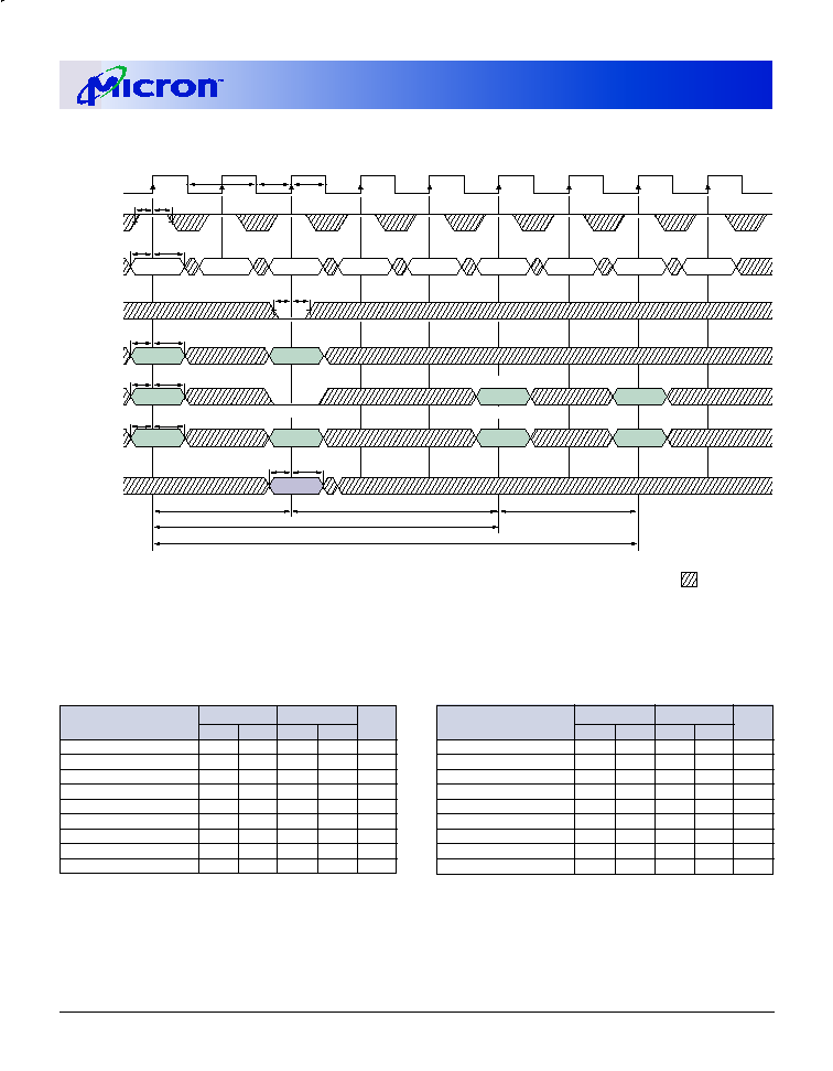
54
128Mb: x16, x32 Mobile SDRAM
Micron Technology, Inc., reserves the right to change products or specifications without notice.
MobileY95W_3V_F.p65 � Rev. F; Pub. 9/02
�2002, Micron Technology, Inc.
128Mb: x16, x32
MOBILE SDRAM
ADVANCE
NOTE: 1. For this example, the burst length = 1, and the WRITE burst is followed by a "manual" PRECHARGE.
2. 15ns is required between <D
IN
m> and the PRECHARGE command, regardless of frequency.
3. x16: A9 and A11 = "Don't Care"
x32: A8, A9,and A11 = "Don't Care"
4. PRECHARGE command not allowed else
t
RAS would be violated.
*CAS latency indicated in parentheses.
-8
-10
SYMBOL*
MIN
MAX
MIN
MAX
UNITS
t
CMH
1
1
ns
t
CMS
2.5
2.5
ns
t
DH
1
1
ns
t
DS
2.5
2.5
ns
t
RAS
48
120,000
50
120,000
ns
t
RC
80
100
ns
t
RCD
20
20
ns
t
RP
20
20
ns
t
WR
15
15
ns
TIMING PARAMETERS
-8
-10
SYMBOL*
MIN
MAX
MIN
MAX
UNITS
t
AH
1
1
ns
t
AS
2.5
2.5
ns
t
CH
3
3
ns
t
CL
3
3
ns
t
CK (3)
8
10
ns
t
CK (2)
10
12
ns
t
CK (1)
20
25
ns
t
CKH
1
1
ns
t
CKS
2.5
2.5
ns
SINGLE WRITE � WITHOUT AUTO PRECHARGE
1
DISABLE AUTO PRECHARGE
ALL BANKS
tCH
tCL
tCK
tRP
tRAS
tRCD
tRC
DQMU, DQML
CKE
CLK
A0-A9, A11
DQ
BA0, BA1
A10
tCMH
tCMS
tAH
tAS
ROW
BANK BANK
BANK
ROW
ROW
BANK
t WR
D
IN
m
tDH
tDS
COMMAND
tCMH
tCMS
NOP
4
NOP
4
PRECHARGE
ACTIVE
NOP
WRITE
ACTIVE
NOP
NOP
tAH
tAS
tAH
tAS
SINGLE BANK
tCKH
tCKS
COLUMN m 3
2
T0
T1
T2
T4
T3
T5
T6
T7
T8
DON'T CARE
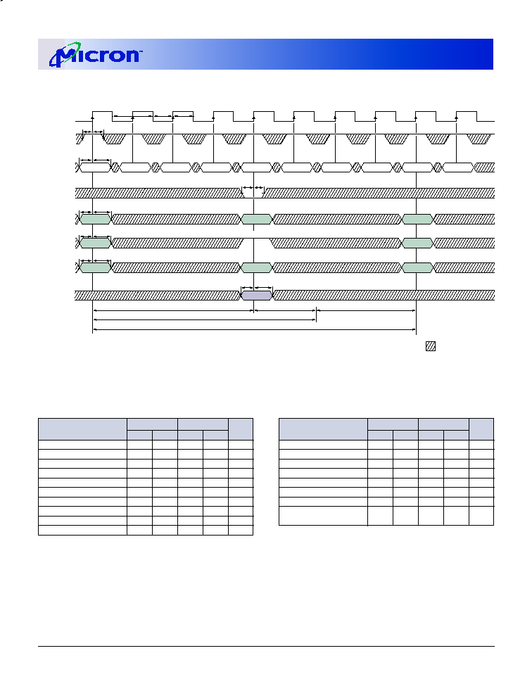
55
128Mb: x16, x32 Mobile SDRAM
Micron Technology, Inc., reserves the right to change products or specifications without notice.
MobileY95W_3V_F.p65 � Rev. F; Pub. 9/02
�2002, Micron Technology, Inc.
128Mb: x16, x32
MOBILE SDRAM
ADVANCE
NOTE: 1. For this example, the burst length = 1.
2. x16: A9 and A11 = "Don't Care"
x32: A8, A9,and A11 = "Don't Care"
3. WRITE command not allowed else
t
RAS would be violated.
ENABLE AUTO PRECHARGE
tCH
tCL
tCK
tRP
tRAS
tRCD
tRC
DQMU, DQML
CKE
CLK
A0-A9, A11
DQ
BA0, BA1
A10
tCMH
tCMS
tAH
tAS
ROW
ROW
BANK
BANK
ROW
ROW
BANK
tWR
D
IN
m
COMMAND
tCMH
tCMS
NOP3
NOP3
NOP
ACTIVE
NOP3
WRITE
NOP
ACTIVE
tAH
tAS
tAH
tAS
tDH
tDS
tCKH
tCKS
NOP
NOP
COLUMN m 2
T0
T1
T2
T4
T3
T5
T6
T7
T8
T9
DON'T CARE
SINGLE WRITE � WITH AUTO PRECHARGE
1
*CAS latency indicated in parentheses.
-8
-10
SYMBOL*
MIN
MAX
MIN
MAX
UNITS
t
CMS
2.5
2.5
ns
t
DH
1
1
ns
t
DS
2.5
2.5
ns
t
RAS
48
120,000
50
120,000
ns
t
RC
80
100
ns
t
RCD
20
20
ns
t
RP
20
20
ns
t
WR
1 CLK +
1 CLK +
�
7ns
5ns
TIMING PARAMETERS
-8
-10
SYMBOL*
MIN
MAX
MIN
MAX
UNITS
t
AH
1
1
ns
t
AS
2.5
2.5
ns
t
CH
3
3
ns
t
CL
3
3
ns
t
CK (3)
8
10
ns
t
CK (2)
10
12
ns
t
CK (1)
20
25
ns
t
CKH
1
1
ns
t
CKS
2.5
2.5
ns
t
CMH
1
1
ns

56
128Mb: x16, x32 Mobile SDRAM
Micron Technology, Inc., reserves the right to change products or specifications without notice.
MobileY95W_3V_F.p65 � Rev. F; Pub. 9/02
�2002, Micron Technology, Inc.
128Mb: x16, x32
MOBILE SDRAM
ADVANCE
ALTERNATING BANK WRITE ACCESSES
1
DON'T CARE
tCH
tCL
tCK
CLK
DQ
D
IN
m
tDH
tDS
D
IN
m + 1
D
IN
m + 2
D
IN
m + 3
COMMAND
tCMH
tCMS
NOP
NOP
ACTIVE
NOP
WRITE
NOP
NOP
ACTIVE
tDH
tDS
tDH
tDS
tDH
tDS
ACTIVE
WRITE
D
IN
b
tDH
tDS
D
IN
b + 1
D
IN
b + 3
tDH
tDS
tDH
tDS
ENABLE AUTO PRECHARGE
DQMU, DQML
A0-A9, A11
BA0, BA1
A10
tCMH
tCMS
tAH
tAS
tAH
tAS
tAH
tAS
ROW
ROW
ROW
ROW
ENABLE AUTO PRECHARGE
ROW
ROW
BANK 0
BANK 0
BANK 1
BANK 0
BANK 1
CKE
tCKH
tCKS
D
IN
b + 2
tDH
tDS
COLUMN b 2
COLUMN m 2
tRP - BANK 0
tRAS - BANK 0
tRCD - BANK 0
t
t
RCD - BANK 0
tWR - BANK 0
WR - BANK 1
tRCD - BANK 1
t
t
RC - BANK 0
RRD
T0
T1
T2
T3
T4
T5
T6
T7
T8
T9
NOTE: 1. For this example, the burst length = 4.
2. x16: A9 and A11 = "Don't Care"
x32: A8, A9,and A11 = "Don't Care"
*CAS latency indicated in parentheses.
-8
-10
SYMBOL*
MIN
MAX
MIN
MAX
UNITS
t
CMS
2.5
2.5
ns
t
DH
1
1
ns
t
DS
2.5
2.5
ns
t
RAS
48
120,000
50
120,000
ns
t
RC
80
100
ns
t
RCD
20
20
ns
t
RP
20
20
ns
t
RRD
20
20
ns
t
WR
1 CLK +
1 CLK +
�
7ns
5ns
TIMING PARAMETERS
-8
-10
SYMBOL*
MIN
MAX
MIN
MAX
UNITS
t
AH
1
1
ns
t
AS
2.5
2.5
ns
t
CH
3
3
ns
t
CL
3
3
ns
t
CK (3)
8
10
ns
t
CK (2)
10
12
ns
t
CK (1)
20
25
ns
t
CKH
1
1
ns
t
CKS
2.5
2.5
ns
t
CMH
1
1
ns
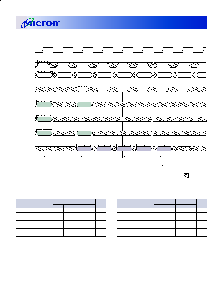
57
128Mb: x16, x32 Mobile SDRAM
Micron Technology, Inc., reserves the right to change products or specifications without notice.
MobileY95W_3V_F.p65 � Rev. F; Pub. 9/02
�2002, Micron Technology, Inc.
128Mb: x16, x32
MOBILE SDRAM
ADVANCE
WRITE � FULL-PAGE BURST
tCH
tCL
tCK
tRCD
DQMU, DQML
CKE
CLK
A0-A9, A11
BA0, BA1
A10
tCMS
tAH
tAS
tAH
tAS
ROW
ROW
Full-page burst does not
self-terminate. Can use
BURST TERMINATE
command to stop.
2, 3
(
)
(
)
(
)
(
)
(
)
(
)
(
)
(
)
Full page completed
DON'T CARE
COMMAND
tCMH
tCMS
NOP
NOP
NOP
ACTIVE
NOP
WRITE
BURST TERM
NOP
NOP
(
)
(
)
(
)
(
)
(
)
(
)
(
)
(
)
DQ
D
IN
m
tDH
tDS
D
IN
m + 1
D
IN
m + 2
D
IN
m + 3
tDH
tDS
tDH
tDS
tDH
tDS
D
IN
m - 1
tDH
tDS
tAH
tAS
BANK
(
)
(
)
(
)
(
)
BANK
tCMH
tCKH
tCKS
(
)
(
)
(
)
(
)
(
)
(
)
(
)
(
)
(
)
(
)
(
)
(
)
512 (x16) locations within same row
COLUMN m 1
T0
T1
T2
T3
T4
T5
Tn + 1
Tn + 2
Tn + 3
NOTE: 1. x16: A9 and A11 = "Don't Care"
x32: A8, A9,and A11 = "Don't Care"
2.
t
WR must be satisfied prior to PRECHARGE command.
3. Page left open; no
t
RP.
*CAS latency indicated in parentheses.
-8
-10
SYMBOL*
MIN
MAX
MIN
MAX
UNITS
t
CKH
1
1
ns
t
CKS
2.5
2.5
ns
t
CMH
1
1
ns
t
CMS
2.5
2.5
ns
t
DH
1
1
ns
t
DS
2.5
2.5
ns
t
RCD
20
20
ns
TIMING PARAMETERS
-8
-10
SYMBOL*
MIN
MAX
MIN
MAX
UNITS
t
AH
1
1
ns
t
AS
2.5
2.5
ns
t
CH
3
3
ns
t
CL
3
3
ns
t
CK (3)
8
10
ns
t
CK (2)
10
12
ns
t
CK (1)
20
25
ns

58
128Mb: x16, x32 Mobile SDRAM
Micron Technology, Inc., reserves the right to change products or specifications without notice.
MobileY95W_3V_F.p65 � Rev. F; Pub. 9/02
�2002, Micron Technology, Inc.
128Mb: x16, x32
MOBILE SDRAM
ADVANCE
WRITE � DQM OPERATION
1
DON'T CARE
tCH
tCL
tCK
tRCD
DQMU, DQML
CKE
CLK
A0-A9, A11
DQ
BA0, BA1
A10
tCMS
tAH
tAS
ROW
BANK
ROW
BANK
ENABLE AUTO PRECHARGE
D
IN
m + 3
tDH
tDS
D
IN
m
D
IN
m + 2
tCMH
COMMAND
NOP
NOP
NOP
ACTIVE
NOP
WRITE
NOP
NOP
tCMS
tCMH
tDH
tDS
tDH
tDS
tAH
tAS
tAH
tAS
DISABLE AUTO PRECHARGE
tCKH
tCKS
COLUMN m 2
T0
T1
T2
T3
T4
T5
T6
T7
NOTE: 1. For this example, the burst length = 4.
2. x16: A9 and A11 = "Don't Care"
x32: A8, A9,and A11 = "Don't Care"
*CAS latency indicated in parentheses.
-8
-10
SYMBOL*
MIN
MAX
MIN
MAX
UNITS
t
CKH
1
1
ns
t
CKS
2.5
2.5
ns
t
CMH
1
1
ns
t
CMS
2.5
2.5
ns
t
DH
1
1
ns
t
DS
2.5
2.5
ns
t
RCD
20
20
ns
TIMING PARAMETERS
-8
-10
SYMBOL*
MIN
MAX
MIN
MAX
UNITS
t
AH
1
1
ns
t
AS
2.5
2.5
ns
t
CH
3
3
ns
t
CL
3
3
ns
t
CK (3)
8
10
ns
t
CK (2)
10
12
ns
t
CK (1)
20
25
ns
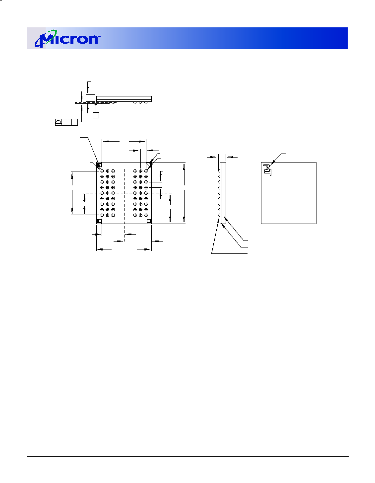
59
128Mb: x16, x32 Mobile SDRAM
Micron Technology, Inc., reserves the right to change products or specifications without notice.
MobileY95W_3V_F.p65 � Rev. F; Pub. 9/02
�2002, Micron Technology, Inc.
128Mb: x16, x32
MOBILE SDRAM
ADVANCE
54-BALL VFBGA (8mm x 9mm)
NOTE: 1. All dimensions in millimeters.
2. Package width and length do not include mold protrusion; allowable mold protrusion is 0.25mm per side.
BALL A1
0.80
TYP
BALL A9
BALL
A1 ID
54X
0.35
SOLDER BALL DIAMETER
REFERS TO POST REFLOW
CONDITION. THE PRE-
REFLOW DIAMETER IS � 0.33
0.80
TYP
6.40
0.70 �0.075
SEATING PLANE
C
0.08 C
1.0 MAX
MOLD COMPOUND: EPOXY NOVOLAC
SUBSTRATE: PLASTIC LAMINATE
SOLDER BALL MATERIAL: EUTECTIC 63% Sn, 37% Pb or
62% Sn, 36% Pb, 2%Ag
SOLDER BALL PAD: � .27mm
4.00 �0.05
3.20 �0.05
3.20 �0.05
8.00 �0.10
BALL A1 ID
4.50 �0.05
9.00 �0.10
6.40
C
L
C
L
60
128Mb: x16, x32 Mobile SDRAM
Micron Technology, Inc., reserves the right to change products or specifications without notice.
MobileY95W_3V_F.p65 � Rev. F; Pub. 9/02
�2002, Micron Technology, Inc.
128Mb: x16, x32
MOBILE SDRAM
ADVANCE
90-BALL FBGA (11mm x 13mm)
(Bottom View)
NOTE: 1. All dimensions in millimeters.
2. Recommended pad size for PCB is 0.33mm�0.025mm.
BALL
A1 ID
SUBSTRATE: PLASTIC LAMINATE
ENCAPSULATION MATERIAL: EPOXY NOVOLAC
SOLDER BALL MATERIAL: EUTECTIC 63% Sn, 37% Pb.
Or 62% Sn, 36% Pb, 2% Ag
SOLDER BALL PAD: � .33mm
SEATING PLANE
.850 �.075
BALL A9
SOLDER BALL DIAMETER REFERS
TO POST REFLOW CONDITION.
THE PRE-REFLOW DIAMETER IS � 0.40mm
.10
C
C
13.00 � .10
.80
TYP
11.20
1.20 MAX
5.60 �.05
6.50 �.05
BALL
A1 ID
BALL A1
.80
TYP
5.50 �.05
3.20 �.05
11.00 �.10
6.40
0.45
90X �
C
L
C
L
61
128Mb: x16, x32 Mobile SDRAM
Micron Technology, Inc., reserves the right to change products or specifications without notice.
MobileY95W_3V_F.p65 � Rev. F; Pub. 9/02
�2002, Micron Technology, Inc.
128Mb: x16, x32
MOBILE SDRAM
ADVANCE
FBGA DEVICE MARKING
Due to the size of the package, Micron's standard part
number is not printed on the top of each device. Instead,
an abbreviated device mark comprised of a five-digit
alphanumeric code is used. The abbreviated device marks
are cross referenced to Micron part numbers in Table 1.
8000 S. Federal Way, P.O. Box 6, Boise, ID 83707-0006, Tel: 208-368-3900
E-mail: prodmktg@micron.com, Internet: http://www.micron.com, Customer Comment Line: 800-932-4992
Micron and the M logo are registered trademarks and the Micron logo is a trademark of Micron Technology, Inc.
DBFCF
Speed Grade
B = -10
C = -8
Width ( I/Os)
D = x16
G = x32
Device Density
F = 128Mb
Product Type
N = 2.5V SDR SDRAM, Low Power version (54-ball, 8 x 9)
P = 3.3V SDR SDRAM, Low Power version (54-ball, 8 x 9)
V = 2.5V SDR SDRAM, Low Power version (90-ball, 11 x 13)
Z = 3.3V SDR SDRAM, Low Power version (90-ball, 11 x 13)
Product Group
D = DRAM
Z = DRAM ENGINEERING SAMPLE
DATA SHEET DESIGNATION
Advance: This data sheet contains initial descriptions of products still under development.
CROSS REFERENCE FOR FBGA OR VFBGA DEVICE MARKING
ENGINEERING
PRODUCTION
PART NUMBER
ARCHITECTURE
FBGA/VFBGA
SAMPLE
MARKING
MT48V4M32LFFC-8
4 Meg x 32
90-pin, 11 x 13
ZVFGC
DVFGC
MT48LC4M32LFFC-10
4 Meg x 32
90-pin, 11 x 13
ZZFGB
DZFGB
MT48V8M16LFFF-10
8 Meg x 16
54-ball, 8 x 9
ZNFDB
DNFDB
MT48LC8M16LFFF-8
8 Meg x 16
54-ball, 8 x 9
ZPFDC
DPFDC