Document Outline
- 288Mb CIO Reduced Latency (RLDRAMÆ II)
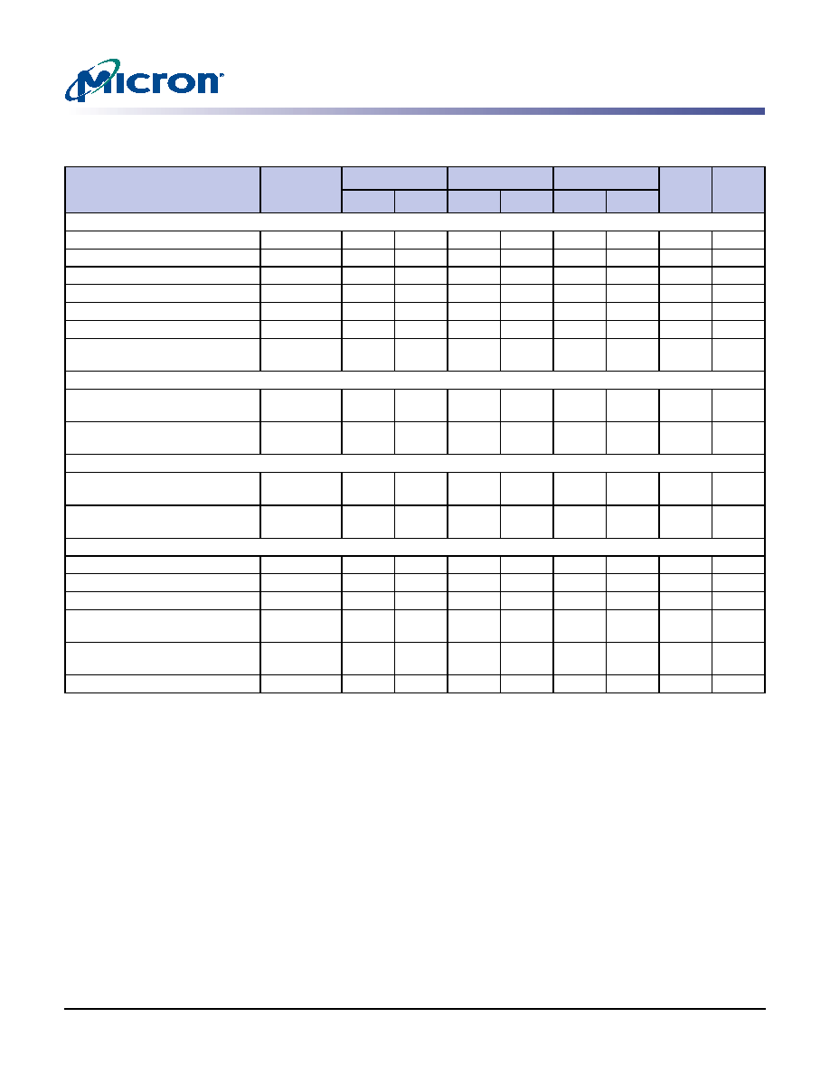
- Table 1: Valid Part Numbers
- Figure 1: 144-Ball µBGA
- Options
- Marking
- General Description
- Functional Block Diagram
- Ball Assignment and Description
- Commands
- Initialization
- Programmable Impedance Output Buffer
- Clock Considerations
- Mode Register Set Command (MRS)
- Configuration Table
- Write Basic Information
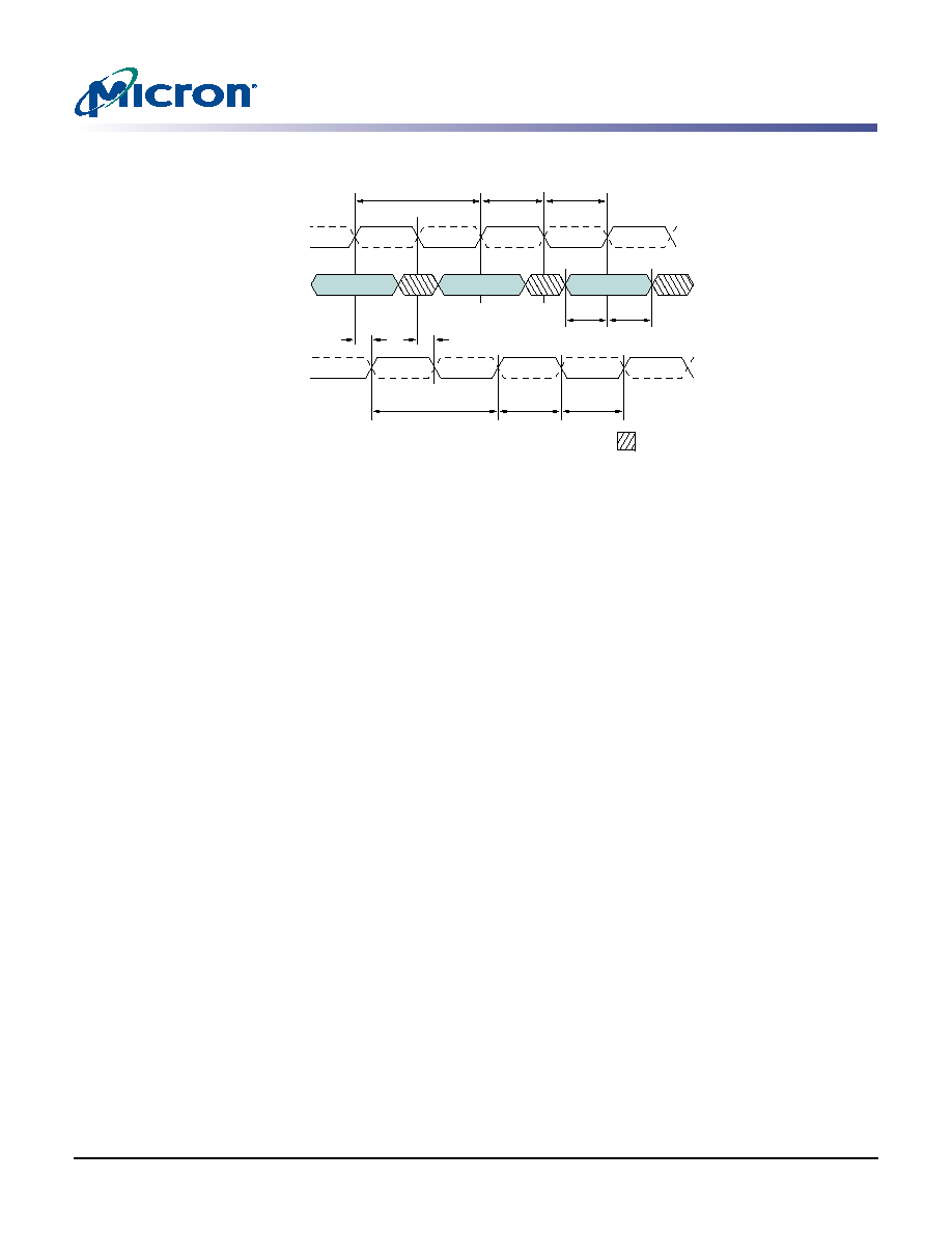
- Figure 9: WRITE Command
- Figure 10: Basic WRITE Burst/DM Timing
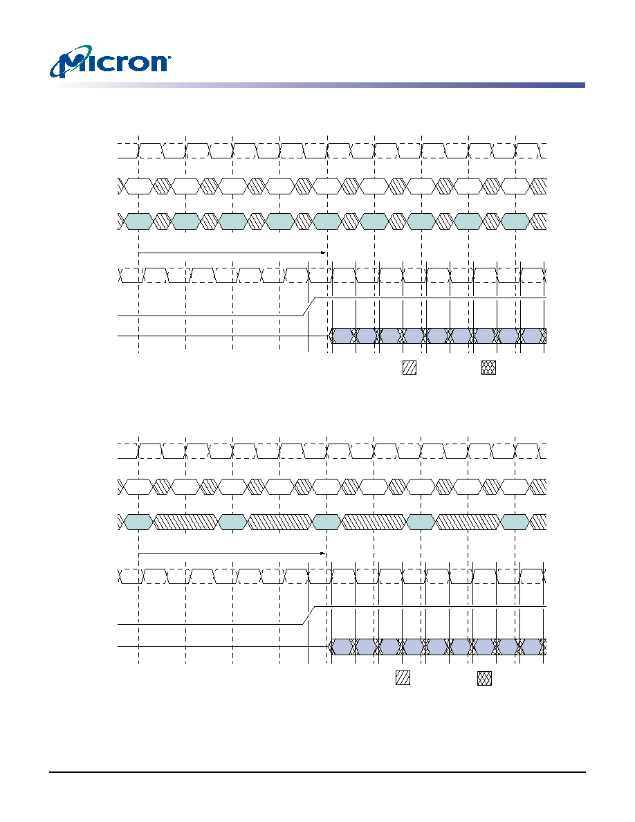
- Figure 11: WRITE Burst Basic Sequence: BL = 2, RL = 4, WL = 5, Configuration 1
- Figure 12: WRITE Burst Basic Sequence: BL = 4, RL = 4, WL = 5, Configuration 1
- Figure 13: WRITE Followed By READ: BL = 2, RL = 4, WL = 5, Configuration 1
- Figure 14: WRITE Followed By READ: BL = 4, RL = 4, WL = 5, Configuration 1
- Read Basic Information
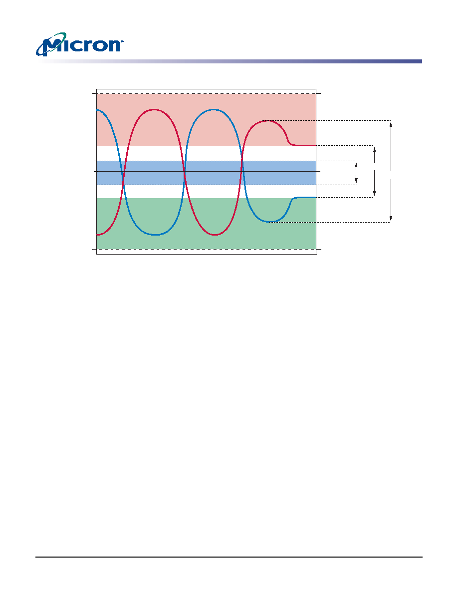
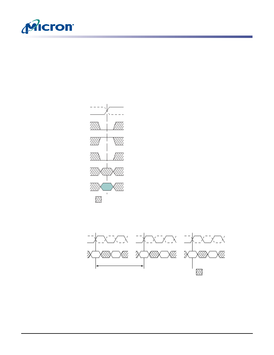
- Figure 15: READ Command
- Figure 16: Basic READ Burst Timing
- Figure 17: READ Burst: BL = 2, RL = 4, Configuration 1
- Figure 18: READ Burst: BL = 4, RL = 4, Configuration 1
- Figure 19: READ followed by WRITE, BL = 2, RL = 4, WL = 5, Configuration 1
- Figure 20: READ followed by WRITE, BL = 4, RL = 4, WL = 5, Configuration 1
- AUTO REFRESH Command (AREF)
- On-Die Termination
- Operation with Multiplexed Addresses
- Address Mapping
- Configuration Table
- REFRESH Command in Multiplexed Address Mode
- IEEE 1149.1 Serial Boundary Scan (JTAG)
- Disabling the JTAG Feature
- Test Access Port (TAP)
- TAP Instruction Set
- Electrical Characteristics
- Package Dimensions
Products and specifications discussed herein are subject to change by Micron without notice.
288Mb: x36, x18, x9 2.5V V
EXT
, 1.8V V
DD
, HSTL, RLDRAM II
Features
PDF: 09005aef80a41b46/Source: 09005aef809f284b
Micron Technology, Inc., reserves the right to change products or specifications without notice.
MT49H8M36_1.fm - Rev. H 8/05 EN
1
©2002 Micron Technology, Inc. All rights reserved.
288Mb CIO Reduced Latency (RLDRAM
Æ
II)
MT49H8M36
MT49H16M18
MT49H32M9
For the latest data sheet, refer to Micron's Web site: www.micron.com/rldram
Features
∑ 400 MHz DDR operation (800 Mb/s/pin data rate)
∑ Organization
8 Meg x 36, 16 Meg x 18, and 32 Meg x 9
8 banks
∑ Cyclic bank switching for maximum bandwidth
∑ Reduced cycle time (20ns at 400 MHz)
∑ Nonmultiplexed addresses (address multiplexing
option available)
∑ SRAM-type interface
∑ Programmable READ latency (RL), row cycle time,
and burst sequence length
∑ Balanced READ and WRITE latencies in order to
optimize data bus utilization
∑ Data mask for WRITE commands
∑ Differential input clocks (CK, CK#)
∑ Differential input data clocks (DKx, DKx#)
∑ On-chip DLL generates CK edge-aligned data and
output data clock signals
∑ Data valid signal (QVLD)
∑ 32ms refresh (8K refresh for each bank; 64K refresh
command must be issued in total each 32ms)
∑ 144-ball µBGA package
∑ HSTL I/O (1.5V or 1.8V nominal)
∑ 25≠60 matched impedance outputs
∑ 2.5V V
EXT
, 1.8V V
DD
, 1.5V or 1.8V V
DD
Q I/O
∑ On-die termination (ODT) R
TT
Table 1:
Valid Part Numbers
Part Number
Description
MT49H8M36FM-xx
8 Meg x 36 RLDRAM II
MT49H16M18FM-xx
16 Meg x 18 RLDRAM II
MT49H32M9FM-xx
32 Meg x 9 RLDRAM II
Figure 1:
144-Ball µBGA
Notes: 1. Contact Micron for availability of lead-free
products.
Options
Marking
∑ Clock cycle timing
2.5ns (400 MHz)
3.3ns (300 MHz)
5ns (200 MHz)
-25
-33
-5
∑ Configuration
8 Meg x 36
16 Meg x 18
32 Meg x 9
MT49H8M36
MT49H16M18
MT49H32M9
∑ Operating temperature range
Commercial
0∞ to +95∞C
Industrial
T
C
= -40∞C to +95∞C
T
A
= -40∞C to 85∞C)
None
IT
∑ Package
144-ball µBGA
(11mm x 18.5mm, lead-free)
FM
BM
1

PDF: 09005aef80a41b46/Source: 09005aef809f284b
Micron Technology, Inc., reserves the right to change products or specifications without notice.
MT49H8M36TOC.fm - Rev. H 8/05 EN
2
©2002 Micron Technology, Inc. All rights reserved.
288Mb: x36, x18, x9 2.5V V
EXT
, 1.8V V
DD
, HSTL, RLDRAM II
Table of Contents
Table of Contents
Features . . . . . . . . . . . . . . . . . . . . . . . . . . . . . . . . . . . . . . . . . . . . . . . . . . . . . . . . . . . . . . . . . . . . . . . . . . . . . . . . . . . . . . . . . . . . . .1
Options . . . . . . . . . . . . . . . . . . . . . . . . . . . . . . . . . . . . . . . . . . . . . . . . . . . . . . . . . . . . . . . . . . . . . . . . . . . . . . . . . . . . . . . . . . . .1
General Description . . . . . . . . . . . . . . . . . . . . . . . . . . . . . . . . . . . . . . . . . . . . . . . . . . . . . . . . . . . . . . . . . . . . . . . . . . . . . . . . . . .5
Functional Block Diagram. . . . . . . . . . . . . . . . . . . . . . . . . . . . . . . . . . . . . . . . . . . . . . . . . . . . . . . . . . . . . . . . . . . . . . . . . . . . . .6
Ball Assignment and Description . . . . . . . . . . . . . . . . . . . . . . . . . . . . . . . . . . . . . . . . . . . . . . . . . . . . . . . . . . . . . . . . . . . . . . .7
Commands . . . . . . . . . . . . . . . . . . . . . . . . . . . . . . . . . . . . . . . . . . . . . . . . . . . . . . . . . . . . . . . . . . . . . . . . . . . . . . . . . . . . . . . . . .11
Initialization . . . . . . . . . . . . . . . . . . . . . . . . . . . . . . . . . . . . . . . . . . . . . . . . . . . . . . . . . . . . . . . . . . . . . . . . . . . . . . . . . . . . . . . . .14
Programmable Impedance Output Buffer. . . . . . . . . . . . . . . . . . . . . . . . . . . . . . . . . . . . . . . . . . . . . . . . . . . . . . . . . . . . . . .15
Clock Considerations . . . . . . . . . . . . . . . . . . . . . . . . . . . . . . . . . . . . . . . . . . . . . . . . . . . . . . . . . . . . . . . . . . . . . . . . . . . . . . . . .15
Mode Register Set Command (MRS). . . . . . . . . . . . . . . . . . . . . . . . . . . . . . . . . . . . . . . . . . . . . . . . . . . . . . . . . . . . . . . . . . . .17
Configuration Table . . . . . . . . . . . . . . . . . . . . . . . . . . . . . . . . . . . . . . . . . . . . . . . . . . . . . . . . . . . . . . . . . . . . . . . . . . . . . . . . . .18
Write Basic Information. . . . . . . . . . . . . . . . . . . . . . . . . . . . . . . . . . . . . . . . . . . . . . . . . . . . . . . . . . . . . . . . . . . . . . . . . . . . . . .19
Read Basic Information . . . . . . . . . . . . . . . . . . . . . . . . . . . . . . . . . . . . . . . . . . . . . . . . . . . . . . . . . . . . . . . . . . . . . . . . . . . . . . .22
AUTO REFRESH Command (AREF) . . . . . . . . . . . . . . . . . . . . . . . . . . . . . . . . . . . . . . . . . . . . . . . . . . . . . . . . . . . . . . . . . . . .26
On-Die Termination . . . . . . . . . . . . . . . . . . . . . . . . . . . . . . . . . . . . . . . . . . . . . . . . . . . . . . . . . . . . . . . . . . . . . . . . . . . . . . . . . .27
Operation with Multiplexed Addresses . . . . . . . . . . . . . . . . . . . . . . . . . . . . . . . . . . . . . . . . . . . . . . . . . . . . . . . . . . . . . . . . .30
Address Mapping . . . . . . . . . . . . . . . . . . . . . . . . . . . . . . . . . . . . . . . . . . . . . . . . . . . . . . . . . . . . . . . . . . . . . . . . . . . . . . . . . . . .33
Configuration Table . . . . . . . . . . . . . . . . . . . . . . . . . . . . . . . . . . . . . . . . . . . . . . . . . . . . . . . . . . . . . . . . . . . . . . . . . . . . . . . . . .34
REFRESH Command in Multiplexed Address Mode . . . . . . . . . . . . . . . . . . . . . . . . . . . . . . . . . . . . . . . . . . . . . . . . . . . . . .34
IEEE 1149.1 Serial Boundary Scan (JTAG) . . . . . . . . . . . . . . . . . . . . . . . . . . . . . . . . . . . . . . . . . . . . . . . . . . . . . . . . . . . . . . .36
Disabling the JTAG Feature. . . . . . . . . . . . . . . . . . . . . . . . . . . . . . . . . . . . . . . . . . . . . . . . . . . . . . . . . . . . . . . . . . . . . . . . . . . .36
Test Access Port (TAP) . . . . . . . . . . . . . . . . . . . . . . . . . . . . . . . . . . . . . . . . . . . . . . . . . . . . . . . . . . . . . . . . . . . . . . . . . . . . . . . .36
Test Clock (TCK) . . . . . . . . . . . . . . . . . . . . . . . . . . . . . . . . . . . . . . . . . . . . . . . . . . . . . . . . . . . . . . . . . . . . . . . . . . . . . . . . . . .36
Test Mode Select (TMS) . . . . . . . . . . . . . . . . . . . . . . . . . . . . . . . . . . . . . . . . . . . . . . . . . . . . . . . . . . . . . . . . . . . . . . . . . . . .36
Test Data-In (TDI) . . . . . . . . . . . . . . . . . . . . . . . . . . . . . . . . . . . . . . . . . . . . . . . . . . . . . . . . . . . . . . . . . . . . . . . . . . . . . . . . .36
Test Data-Out (TDO) . . . . . . . . . . . . . . . . . . . . . . . . . . . . . . . . . . . . . . . . . . . . . . . . . . . . . . . . . . . . . . . . . . . . . . . . . . . . . . .36
Performing a TAP RESET . . . . . . . . . . . . . . . . . . . . . . . . . . . . . . . . . . . . . . . . . . . . . . . . . . . . . . . . . . . . . . . . . . . . . . . . . . .37
TAP Registers. . . . . . . . . . . . . . . . . . . . . . . . . . . . . . . . . . . . . . . . . . . . . . . . . . . . . . . . . . . . . . . . . . . . . . . . . . . . . . . . . . . . . .37
Instruction Register . . . . . . . . . . . . . . . . . . . . . . . . . . . . . . . . . . . . . . . . . . . . . . . . . . . . . . . . . . . . . . . . . . . . . . . . . . . . . . . .38
Bypass Register . . . . . . . . . . . . . . . . . . . . . . . . . . . . . . . . . . . . . . . . . . . . . . . . . . . . . . . . . . . . . . . . . . . . . . . . . . . . . . . . . . . .38
Boundary Scan Register . . . . . . . . . . . . . . . . . . . . . . . . . . . . . . . . . . . . . . . . . . . . . . . . . . . . . . . . . . . . . . . . . . . . . . . . . . . .38
Identification (ID) Register. . . . . . . . . . . . . . . . . . . . . . . . . . . . . . . . . . . . . . . . . . . . . . . . . . . . . . . . . . . . . . . . . . . . . . . . . .38
TAP Instruction Set . . . . . . . . . . . . . . . . . . . . . . . . . . . . . . . . . . . . . . . . . . . . . . . . . . . . . . . . . . . . . . . . . . . . . . . . . . . . . . . . . . .38
Overview. . . . . . . . . . . . . . . . . . . . . . . . . . . . . . . . . . . . . . . . . . . . . . . . . . . . . . . . . . . . . . . . . . . . . . . . . . . . . . . . . . . . . . . . . .38
EXTEST . . . . . . . . . . . . . . . . . . . . . . . . . . . . . . . . . . . . . . . . . . . . . . . . . . . . . . . . . . . . . . . . . . . . . . . . . . . . . . . . . . . . . . . . . . .39
IDCODE . . . . . . . . . . . . . . . . . . . . . . . . . . . . . . . . . . . . . . . . . . . . . . . . . . . . . . . . . . . . . . . . . . . . . . . . . . . . . . . . . . . . . . . . . .39
High-Z. . . . . . . . . . . . . . . . . . . . . . . . . . . . . . . . . . . . . . . . . . . . . . . . . . . . . . . . . . . . . . . . . . . . . . . . . . . . . . . . . . . . . . . . . . . .39
CLAMP . . . . . . . . . . . . . . . . . . . . . . . . . . . . . . . . . . . . . . . . . . . . . . . . . . . . . . . . . . . . . . . . . . . . . . . . . . . . . . . . . . . . . . . . . . .39
SAMPLE/PRELOAD . . . . . . . . . . . . . . . . . . . . . . . . . . . . . . . . . . . . . . . . . . . . . . . . . . . . . . . . . . . . . . . . . . . . . . . . . . . . . . . .39
BYPASS . . . . . . . . . . . . . . . . . . . . . . . . . . . . . . . . . . . . . . . . . . . . . . . . . . . . . . . . . . . . . . . . . . . . . . . . . . . . . . . . . . . . . . . . . . .39
Reserved for Future Use . . . . . . . . . . . . . . . . . . . . . . . . . . . . . . . . . . . . . . . . . . . . . . . . . . . . . . . . . . . . . . . . . . . . . . . . . . . .39
Electrical Characteristics . . . . . . . . . . . . . . . . . . . . . . . . . . . . . . . . . . . . . . . . . . . . . . . . . . . . . . . . . . . . . . . . . . . . . . . . . . . . . .44
Package Dimensions . . . . . . . . . . . . . . . . . . . . . . . . . . . . . . . . . . . . . . . . . . . . . . . . . . . . . . . . . . . . . . . . . . . . . . . . . . . . . . . . .48

PDF: 09005aef80a41b46/Source: 09005aef809f284b
Micron Technology, Inc., reserves the right to change products or specifications without notice.
MT49H8M36LOF.fm - Rev. H 8/05 EN
3
©2002 Micron Technology, Inc. All rights reserved.
288Mb: x36, x18, x9 2.5V V
EXT
, 1.8V V
DD
, HSTL, RLDRAM II
List of Figures
List of Figures
Figure 1:
144-Ball µBGA . . . . . . . . . . . . . . . . . . . . . . . . . . . . . . . . . . . . . . . . . . . . . . . . . . . . . . . . . . . . . . . . . . . . . . . . . . . .1
Figure 2:
8 Meg x 36 . . . . . . . . . . . . . . . . . . . . . . . . . . . . . . . . . . . . . . . . . . . . . . . . . . . . . . . . . . . . . . . . . . . . . . . . . . . . . . . .6
Figure 3:
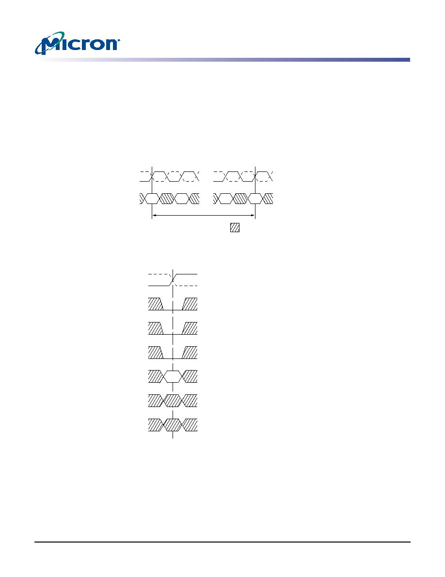
Clock/Input Data Clock Command/Address Timings . . . . . . . . . . . . . . . . . . . . . . . . . . . . . . . . . . . . . . .14
Figure 4:
Power-Up Sequence. . . . . . . . . . . . . . . . . . . . . . . . . . . . . . . . . . . . . . . . . . . . . . . . . . . . . . . . . . . . . . . . . . . . . .15
Figure 5:
Clock Input. . . . . . . . . . . . . . . . . . . . . . . . . . . . . . . . . . . . . . . . . . . . . . . . . . . . . . . . . . . . . . . . . . . . . . . . . . . . . .16
Figure 6:
Mode Register Set Timing . . . . . . . . . . . . . . . . . . . . . . . . . . . . . . . . . . . . . . . . . . . . . . . . . . . . . . . . . . . . . . . .17
Figure 7:
Mode Register Set . . . . . . . . . . . . . . . . . . . . . . . . . . . . . . . . . . . . . . . . . . . . . . . . . . . . . . . . . . . . . . . . . . . . . . .17
Figure 8:
Mode Register Bit Map . . . . . . . . . . . . . . . . . . . . . . . . . . . . . . . . . . . . . . . . . . . . . . . . . . . . . . . . . . . . . . . . . . .18
Figure 9:
WRITE Command . . . . . . . . . . . . . . . . . . . . . . . . . . . . . . . . . . . . . . . . . . . . . . . . . . . . . . . . . . . . . . . . . . . . . . .19
Figure 10:
Basic WRITE Burst/DM Timing. . . . . . . . . . . . . . . . . . . . . . . . . . . . . . . . . . . . . . . . . . . . . . . . . . . . . . . . . . . .20
Figure 11:
WRITE Burst Basic Sequence: BL = 2, RL = 4, WL = 5, Configuration 1 . . . . . . . . . . . . . . . . . . . . . . . . . .20
Figure 12:
WRITE Burst Basic Sequence: BL = 4, RL = 4, WL = 5, Configuration 1 . . . . . . . . . . . . . . . . . . . . . . . . . .21
Figure 13:
WRITE Followed By READ: BL = 2, RL = 4, WL = 5, Configuration 1 . . . . . . . . . . . . . . . . . . . . . . . . . . . .21
Figure 14:
WRITE Followed By READ: BL = 4, RL = 4, WL = 5, Configuration 1 . . . . . . . . . . . . . . . . . . . . . . . . . . . .22
Figure 15:
READ Command . . . . . . . . . . . . . . . . . . . . . . . . . . . . . . . . . . . . . . . . . . . . . . . . . . . . . . . . . . . . . . . . . . . . . . . .23
Figure 16:
Basic READ Burst Timing . . . . . . . . . . . . . . . . . . . . . . . . . . . . . . . . . . . . . . . . . . . . . . . . . . . . . . . . . . . . . . . . .23
Figure 17:
READ Burst: BL = 2, RL = 4, Configuration 1 . . . . . . . . . . . . . . . . . . . . . . . . . . . . . . . . . . . . . . . . . . . . . . . . .24
Figure 18:
READ Burst: BL = 4, RL = 4, Configuration 1 . . . . . . . . . . . . . . . . . . . . . . . . . . . . . . . . . . . . . . . . . . . . . . . . .24
Figure 19:
READ followed by WRITE, BL = 2, RL = 4, WL = 5, Configuration 1 . . . . . . . . . . . . . . . . . . . . . . . . . . . . .25
Figure 20:
READ followed by WRITE, BL = 4, RL = 4, WL = 5, Configuration 1 . . . . . . . . . . . . . . . . . . . . . . . . . . . . .25
Figure 21:
AUTO REFRESH Command . . . . . . . . . . . . . . . . . . . . . . . . . . . . . . . . . . . . . . . . . . . . . . . . . . . . . . . . . . . . . .26
Figure 22:
AUTO REFRESH Cycle . . . . . . . . . . . . . . . . . . . . . . . . . . . . . . . . . . . . . . . . . . . . . . . . . . . . . . . . . . . . . . . . . . . .26
Figure 23:
On-Die Termination-Equivalent Circuit . . . . . . . . . . . . . . . . . . . . . . . . . . . . . . . . . . . . . . . . . . . . . . . . . . .27
Figure 24:
READ Burst with ODT: BL = 2, Configuration 1 . . . . . . . . . . . . . . . . . . . . . . . . . . . . . . . . . . . . . . . . . . . . . .28
Figure 25:
READ NOP READ with ODT: BL = 2, Configuration 1. . . . . . . . . . . . . . . . . . . . . . . . . . . . . . . . . . . . . . . . .28
Figure 26:
READ NOP NOP READ with ODT: BL = 2, Configuration 1 . . . . . . . . . . . . . . . . . . . . . . . . . . . . . . . . . . . .29
Figure 27:
READ followed by WRITE with ODT: BL = 2, Configuration 1 . . . . . . . . . . . . . . . . . . . . . . . . . . . . . . . . .29
Figure 28:
WRITE followed by READ with ODT: BL = 2, Configuration 1 . . . . . . . . . . . . . . . . . . . . . . . . . . . . . . . . .30
Figure 29:
Command Description in Multiplexed Address Mode. . . . . . . . . . . . . . . . . . . . . . . . . . . . . . . . . . . . . . . .31
Figure 30:
Mode Register Set Command in Multiplexed Address Mode . . . . . . . . . . . . . . . . . . . . . . . . . . . . . . . . . .31
Figure 31:
Power-Up Sequence in Multiplexed Address Mode . . . . . . . . . . . . . . . . . . . . . . . . . . . . . . . . . . . . . . . . . .32
Figure 32:
Burst REFRESH Operation . . . . . . . . . . . . . . . . . . . . . . . . . . . . . . . . . . . . . . . . . . . . . . . . . . . . . . . . . . . . . . . .34
Figure 33:
WRITE Burst Basic Sequence: BL = 4, with Multiplexed Addresses, Configuration 1, WL = 6 . . . . . .35
Figure 34:
READ Burst Basic Sequence: BL = 4, with Multiplexed Addresses, Configuration 1, RL = 5. . . . . . . .35
Figure 35:
TAP Controller State Diagram . . . . . . . . . . . . . . . . . . . . . . . . . . . . . . . . . . . . . . . . . . . . . . . . . . . . . . . . . . . . .37
Figure 36:
TAP Controller Block Diagram . . . . . . . . . . . . . . . . . . . . . . . . . . . . . . . . . . . . . . . . . . . . . . . . . . . . . . . . . . . .37
Figure 37:
TAP Timing. . . . . . . . . . . . . . . . . . . . . . . . . . . . . . . . . . . . . . . . . . . . . . . . . . . . . . . . . . . . . . . . . . . . . . . . . . . . . .40
Figure 38:
Absolute Maximum Ratings . . . . . . . . . . . . . . . . . . . . . . . . . . . . . . . . . . . . . . . . . . . . . . . . . . . . . . . . . . . . . .44
Figure 39:
Output Test Conditions . . . . . . . . . . . . . . . . . . . . . . . . . . . . . . . . . . . . . . . . . . . . . . . . . . . . . . . . . . . . . . . . . .45
Figure 40:
Input Waveform . . . . . . . . . . . . . . . . . . . . . . . . . . . . . . . . . . . . . . . . . . . . . . . . . . . . . . . . . . . . . . . . . . . . . . . . .45
Figure 41:
144-Ball µBGA . . . . . . . . . . . . . . . . . . . . . . . . . . . . . . . . . . . . . . . . . . . . . . . . . . . . . . . . . . . . . . . . . . . . . . . . . . .48

PDF: 09005aef80a41b46/Source: 09005aef809f284b
Micron Technology, Inc., reserves the right to change products or specifications without notice.
MT49H8M36LOT.fm - Rev. H 8/05 EN
4
©2002 Micron Technology, Inc. All rights reserved.
288Mb: x36, x18, x9 2.5V V
EXT
, 1.8V V
DD
, HSTL, RLDRAM II
List of Tables
List of Tables
Table 1:
Valid Part Numbers . . . . . . . . . . . . . . . . . . . . . . . . . . . . . . . . . . . . . . . . . . . . . . . . . . . . . . . . . . . . . . . . . . . . . . .1
Table 2:
8 Meg x 36 Ball Assignment (Top View) 144-Ball µBGA . . . . . . . . . . . . . . . . . . . . . . . . . . . . . . . . . . . . . . . .7
Table 3:
16 Meg x 18 Ball Assignment (Top View) 144-Ball µBGA . . . . . . . . . . . . . . . . . . . . . . . . . . . . . . . . . . . . . . .8
Table 4:
32 Meg x 9 Ball Assignment (Top View) 144-Ball µBGA . . . . . . . . . . . . . . . . . . . . . . . . . . . . . . . . . . . . . . . .9
Table 5:
Ball Descriptions. . . . . . . . . . . . . . . . . . . . . . . . . . . . . . . . . . . . . . . . . . . . . . . . . . . . . . . . . . . . . . . . . . . . . . . . .10
Table 7:
Command Table . . . . . . . . . . . . . . . . . . . . . . . . . . . . . . . . . . . . . . . . . . . . . . . . . . . . . . . . . . . . . . . . . . . . . . . . .11
Table 8:
Description of Commands . . . . . . . . . . . . . . . . . . . . . . . . . . . . . . . . . . . . . . . . . . . . . . . . . . . . . . . . . . . . . . . .12
Table 9:
AC Electrical Characteristics . . . . . . . . . . . . . . . . . . . . . . . . . . . . . . . . . . . . . . . . . . . . . . . . . . . . . . . . . . . . . .13
Table 10:
Clock Input Operating Conditions . . . . . . . . . . . . . . . . . . . . . . . . . . . . . . . . . . . . . . . . . . . . . . . . . . . . . . . . .15
Table 11:
RLDRAM Configuration Table . . . . . . . . . . . . . . . . . . . . . . . . . . . . . . . . . . . . . . . . . . . . . . . . . . . . . . . . . . . . .18
Table 13:
Address Mapping in Multiplexed Address Mode. . . . . . . . . . . . . . . . . . . . . . . . . . . . . . . . . . . . . . . . . . . . .33
Table 14:
Configuration Table In Multiplexed Address Mode . . . . . . . . . . . . . . . . . . . . . . . . . . . . . . . . . . . . . . . . . .34
Table 15:
TAP AC Electrical Characteristics and Operating Conditions. . . . . . . . . . . . . . . . . . . . . . . . . . . . . . . . . .40
Table 16:
TAP AC Electrical Characteristics . . . . . . . . . . . . . . . . . . . . . . . . . . . . . . . . . . . . . . . . . . . . . . . . . . . . . . . . . .40
Table 17:
TAP DC Electrical Characteristics and Operating Conditions . . . . . . . . . . . . . . . . . . . . . . . . . . . . . . . . .41
Table 18:
Identification Register Definitions . . . . . . . . . . . . . . . . . . . . . . . . . . . . . . . . . . . . . . . . . . . . . . . . . . . . . . . . .42
Table 19:
Scan Register Sizes . . . . . . . . . . . . . . . . . . . . . . . . . . . . . . . . . . . . . . . . . . . . . . . . . . . . . . . . . . . . . . . . . . . . . . .42
Table 20:
Instruction Codes . . . . . . . . . . . . . . . . . . . . . . . . . . . . . . . . . . . . . . . . . . . . . . . . . . . . . . . . . . . . . . . . . . . . . . . .42
Table 21:
Boundary Scan (Exit) Order . . . . . . . . . . . . . . . . . . . . . . . . . . . . . . . . . . . . . . . . . . . . . . . . . . . . . . . . . . . . . . .43
Table 22:
DC Electrical Characteristics and Operating Conditions. . . . . . . . . . . . . . . . . . . . . . . . . . . . . . . . . . . . . .44
Table 23:
AC Electrical Characteristics and Operating Conditions . . . . . . . . . . . . . . . . . . . . . . . . . . . . . . . . . . . . . .45
Table 24:
Capacitance . . . . . . . . . . . . . . . . . . . . . . . . . . . . . . . . . . . . . . . . . . . . . . . . . . . . . . . . . . . . . . . . . . . . . . . . . . . . .45
Table 25:
I
DD
Operating Conditions and Maximum Limits . . . . . . . . . . . . . . . . . . . . . . . . . . . . . . . . . . . . . . . . . . . .46

PDF: 09005aef80a41b46/Source: 09005aef809f284b
Micron Technology, Inc., reserves the right to change products or specifications without notice.
MT49H8M36_2.fm - Rev. H 8/05 EN
5
©2002 Micron Technology, Inc. All rights reserved.
288Mb: x36, x18, x9 2.5V V
EXT
, 1.8V V
DD
, HSTL, RLDRAM II
General Description
General Description
The Micron
Æ
288Mb reduced latency DRAM (RLDRAM
Æ
) II is a high-speed memory
device designed for high bandwidth communication data storage--telecommunica-
tions, networking, and cache applications, etc. The chip's 8-bank architecture is opti-
mized for high speed and achieves a peak bandwidth of 28.8 Gb/s, using a 36-bit
interface and a maximum system clock of 400 MHz.
The double data rate (DDR) interface transfers two 36-, 18-, or 9-bit wide data word per
clock cycle at the I/O pins. Output data is referenced to the free-running output data
clock.
Commands, addresses, and control signals are registered at every positive edge of the
differential input clock, while input data is registered at both positive and negative edges
of the input data clock(s).
Read and write accesses to the RLDRAM are burst-oriented. The burst length is pro-
grammable from 2, 4, or 8
1
by setting the mode register.
The device is supplied with 2.5V and 1.8V for the core and 1.5V or 1.8V for the output
drivers.
Bank-scheduled refresh is supported with row address generated internally.
A standard µBGA 144-ball package is used to enable ultra high-speed data transfer rates
and a simple upgrade path from former products.
Notes:
1. Burst of 8 on x18 and x9 devices only.
PDF: 09005aef80a41b46/Source: 09005aef809f284b
Micron Technology, Inc., reserves the right to change products or specifications without notice.
MT49H8M36_2.fm - Rev. H 8/05 EN
6
©2002 Micron Technology, Inc. All rights reserved.
288Mb: x36, x18, x9 2.5V V
EXT
, 1.8V V
DD
, HSTL, RLDRAM II
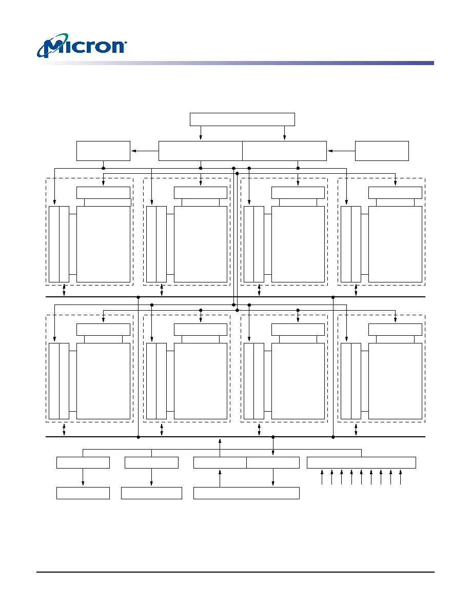
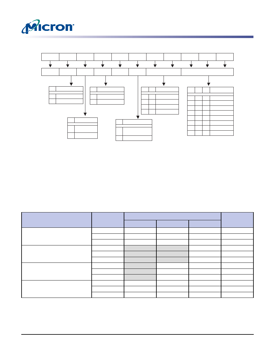
Functional Block Diagram
Functional Block Diagram
Figure 2:
8 Meg x 36
Notes: 1. When the BL = 4 setting is used, A18 is a "Don't Care."
A0≠A18
1
, B0, B1, B2
Column Address
Buffer
Column Address
Counter
Refresh
Counter
Row Decoder
Memory Array
Bank 1
Column Decoder
Sense Amp and Data Bus
Row Address
Buffer
Row Decoder
Memory Array
Bank 0
Column Decoder
Sense Amp and Data Bus
Row Decoder
Memory Array
Bank 2
Column Decoder
Sense Amp and Data Bus
Row Decoder
Memory Array
Bank 3
Column Decoder
Sense Amp and Data Bus
Row Decoder
Memory Array
Bank 5
Column Decoder
Sense Amp and Data Bus
Row Decoder
Memory Array
Bank 4
Column Decoder
Sense Amp and Data Bus
Row Decoder
Memory Array
Bank 6
Column Decoder
Sense Amp and Data Bus
Row Decoder
Memory Array
Bank 7
Column Decoder
CK
CK#
DK[1:0]
DK#[1:0]
WE#
CS#
REF#
DM
V
REF
Sense Amp and Data Bus
Output Data Valid
QVLD
Output Data Clock
QK[1:0], QK#[1:0]
Input Buffers
Output Buffers
Control Logic and Timing Generator
DQ0≠DQ35
PDF: 09005aef80a41b46/Source: 09005aef809f284b
Micron Technology, Inc., reserves the right to change products or specifications without notice.
MT49H8M36_2.fm - Rev. H 8/05 EN
7
©2002 Micron Technology, Inc. All rights reserved.
288Mb: x36, x18, x9 2.5V V
EXT
, 1.8V V
DD
, HSTL, RLDRAM II
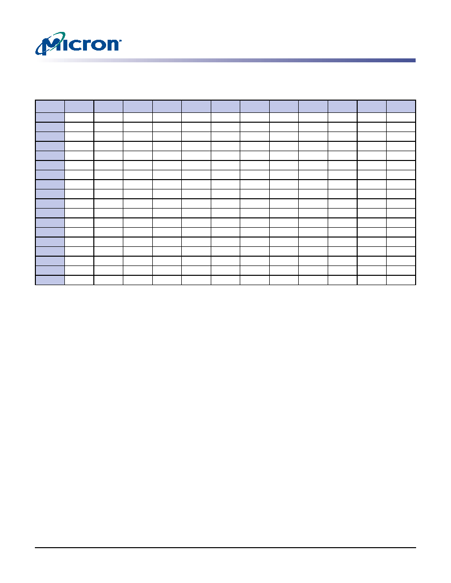
Ball Assignment and Description
Ball Assignment and Description
Table 2:
8 Meg x 36 Ball Assignment (Top View) 144-Ball µBGA
Notes: 1. Reserved for future use. This may optionally be connected to GND.
2. Reserved for future use. This signal is internally connected and has parasitic characteristics
of an address input signal. This may optionally be connected to GND.
1
2
3
4
5
6
7
8
9
10
11
12
A
V
REF
V
SS
V
EXT
V
SS
V
SS
V
EXT
TMS
TCK
B
V
DD
DQ8
DQ9
V
SS
Q
V
SS
Q
DQ1
DQ0
V
DD
C
V
TT
DQ10
DQ11
V
DD
Q
V
DD
Q
DQ3
DQ2
V
TT
D
(A22)
1
DQ12
DQ13
V
SS
Q
V
SS
Q
QK0#
QK0
V
SS
E
(A21)
2
DQ14
DQ15
V
DD
Q
V
DD
Q
DQ5
DQ4
(A20)
2
F
A5
DQ16
DQ17
V
SS
Q
V
SS
Q
DQ7
DQ6
QVLD
G
A8
A6
A7
V
DD
V
DD
A2
A1
A0
H
B2
A9
V
SS
V
SS
V
SS
V
SS
A4
A3
J
DK0
DK0#
V
DD
V
DD
V
DD
V
DD
B0
CK
K
DK1
DK1#
V
DD
V
DD
V
DD
V
DD
B1
CK#
L
REF#
CS#
V
SS
V
SS
V
SS
V
SS
A14
A13
M
WE#
A16
A17
V
DD
V
DD
A12
A11
A10
N
A18
DQ24
DQ25
V
SS
Q
V
SS
Q
DQ35
DQ34
(A19)
2
P
A15
DQ22
DQ23
V
DD
Q
V
DD
Q
DQ33
DQ32
DM
R
V
SS
QK1
QK1#
V
SS
Q
V
SS
Q
DQ31
DQ30
V
SS
T
V
TT
DQ20
DQ21
V
DD
Q
V
DD
Q
DQ29
DQ28
V
TT
U
V
DD
DQ18
DQ19
V
SS
Q
V
SS
Q
DQ27
DQ26
V
DD
V
V
REF
ZQ
V
EXT
V
SS
V
SS
V
EXT
TDO
TDI
PDF: 09005aef80a41b46/Source: 09005aef809f284b
Micron Technology, Inc., reserves the right to change products or specifications without notice.
MT49H8M36_2.fm - Rev. H 8/05 EN
8
©2002 Micron Technology, Inc. All rights reserved.
288Mb: x36, x18, x9 2.5V V
EXT
, 1.8V V
DD
, HSTL, RLDRAM II
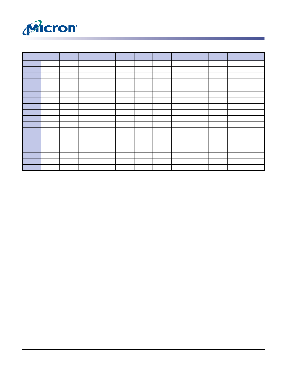
Ball Assignment and Description
Table 3:
16 Meg x 18 Ball Assignment (Top View) 144-Ball µBGA
Notes: 1. Reserved for future use. This may optionally be connected to GND.
2. Reserved for future use. This signal is internally connected and has parasitic characteristics
of an address input signal. This may optionally be connected to GND
3. No Function. This signal is internally connected and has parasitic characteristics of a clock
input signal.
4. Do not use. This signal is internally connected and has parasitic characteristics of a I/O. This
may optionally be connected to GND.
1
2
3
4
5
6
7
8
9
10
11
12
A
V
REF
V
SS
V
EXT
V
SS
V
SS
V
EXT
TMS
TCK
B
V
DD
DNU
4
DQ4
V
SS
Q
V
SS
Q
DQ0
DNU
4
V
DD
C
V
TT
DNU
4
DQ5
V
DD
Q
V
DD
Q
DQ1
DNU
4
V
TT
D
(A22)
1
DNU
4
DQ6
V
SS
Q
V
SS
Q
QK0#
QK0
V
SS
E
(A21)
2
DNU
4
DQ7
V
DD
Q
V
DD
Q
DQ2
DNU
4
(A20)
2
F
A5
DNU
4
DQ8
V
SS
Q
V
SS
Q
DQ3
DNU
4
QVLD
G
A8
A6
A7
V
DD
V
DD
A2
A1
A0
H
B2
A9
V
SS
V
SS
V
SS
V
SS
A4
A3
J
NF
3
NF
3
V
DD
V
DD
V
DD
V
DD
B0
CK
K
DK
DK#
V
DD
V
DD
V
DD
V
DD
B1
CK#
L
REF#
CS#
V
SS
V
SS
V
SS
V
SS
A14
A13
M
WE#
A16
A17
V
DD
V
DD
A12
A11
A10
N
A18
DNU
4
DQ14
V
SS
Q
V
SS
Q
DQ9
DNU
4
A19
P
A15
DNU
4
DQ15
V
DD
Q
V
DD
Q
DQ10
DNU
4
DM
R
V
SS
QK1
QK1#
V
SS
Q
V
SS
Q
DQ11
DNU
4
V
SS
T
V
TT
DNU
4
DQ16
V
DD
Q
V
DD
Q
DQ12
DNU
4
V
TT
U
V
DD
DNU
4
DQ17
V
SS
Q
V
SS
Q
DQ13
DNU
4
V
DD
V
V
REF
ZQ
V
EXT
V
SS
V
SS
V
EXT
TDO
TDI

PDF: 09005aef80a41b46/Source: 09005aef809f284b
Micron Technology, Inc., reserves the right to change products or specifications without notice.
MT49H8M36_2.fm - Rev. H 8/05 EN
9
©2002 Micron Technology, Inc. All rights reserved.
288Mb: x36, x18, x9 2.5V V
EXT
, 1.8V V
DD
, HSTL, RLDRAM II
Ball Assignment and Description
Table 4:
32 Meg x 9 Ball Assignment (Top View) 144-Ball µBGA
Notes: 1. Reserved for future use. This signal is not connected.
2. Reserved for future use. This signal is internally connected and has parasitic characteristics
of a clock input signal.
3. No Function. This signal is internally connected and has parasitic characteristics of a clock
input signal.
4. Do not use. This signal is internally connected and has parasitic characteristics of a I/O. This
may optionally be connected to GND.
1
2
3
4
5
6
7
8
9
10
11
12
A
V
REF
V
SS
V
EXT
V
SS
V
SS
V
EXT
TMS
TCK
B
V
DD
DNU
4
DNU
4
V
SS
Q
V
SS
Q
DQ0
DNU
4
V
DD
C
V
TT
DNU
4
DNU
4
V
DD
Q
V
DD
Q
DQ1
DNU
4
V
TT
D
(A22)
1
DNU
4
DNU
4
V
SS
Q
V
SS
Q
QK0#
QK0
V
SS
E
(A21)
2
DNU
4
DNU
4
V
DD
Q
V
DD
Q
DQ2
DNU
4
A20
F
A5
DNU
4
DNU
4
V
SS
Q
V
SS
Q
DQ3
DNU
4
QVLD
G
A8
A6
A7
V
DD
V
DD
A2
A1
A0
H
B2
A9
V
SS
V
SS
V
SS
V
SS
A4
A3
J
NF
3
NF
3
V
DD
V
DD
V
DD
V
DD
B0
CK
K
DK
DK#
V
DD
V
DD
V
DD
V
DD
B1
CK#
L
REF#
CS#
V
SS
V
SS
V
SS
V
SS
A14
A13
M
WE#
A16
A17
V
DD
V
DD
A12
A11
A10
N
A18
DNU
4
DNU
4
V
SS
Q
V
SS
Q
DQ4
DNU
4
A19
P
A15
DNU
4
DNU
4
V
DD
Q
V
DD
Q
DQ5
DNU
4
DM
R
V
SS
DNU
4
DNU
4
V
SS
Q
V
SS
Q
DQ6
DNU
4
V
SS
T
V
TT
DNU
4
DNU
4
V
DD
Q
V
DD
Q
DQ7
DNU
4
V
TT
U
V
DD
DNU
4
DNU
4
V
SS
Q
V
SS
Q
DQ8
DNU
4
V
DD
V
V
REF
ZQ
V
EXT
V
SS
V
SS
V
EXT
TDO
TDI

PDF: 09005aef80a41b46/Source: 09005aef809f284b
Micron Technology, Inc., reserves the right to change products or specifications without notice.
MT49H8M36_2.fm - Rev. H 8/05 EN
10
©2002 Micron Technology, Inc. All rights reserved.
288Mb: x36, x18, x9 2.5V V
EXT
, 1.8V V
DD
, HSTL, RLDRAM II
Ball Assignment and Description
Table 5:
Ball Descriptions
Symbol
Type
Description
CK, CK#
Input
Input clock: CK and CK# are differential clock inputs. Addresses and commands are latched
on the rising edge of CK. CK# is ideally 180 degrees out of phase with CK.
CS#
Input
Chip select: CS# enables the command decoder when LOW and disables it when HIGH.
When the command decoder is disabled, new commands are ignored, but internal
operations continue.
WE#, REF#
Input
Command inputs: Sampled at the positive edge of CK, WE#, and REF# define (together
with CS#) the command to be executed.
A[0:20]
Input
Address inputs: A[0:20] define the row and column addresses for READ and WRITE
operations. During a MODE REGISTER SET, the address inputs define the register settings.
They are sampled at the rising edge of CK. In the x36 configuration, A[20:19] are reserved
for address expansion; in the x18 configuration, A[20] is reserved for address epansion.
These expansion addresses can be treated as address inputs, but they do not affect the
operation of the device.
A21
≠
Reserved for future use. This signal is internally connected and can be treated as an address
input.
A22
≠
Reserved for future use. This signal is not connected and may be connected to ground.
BA[0:2]
Input
Bank address inputs: Select to which internal bank a command is being applied.
DQ0≠DQ35
Input/Output Data input/output: The DQ signals form the 36-bit data bus. During READ commands, the
data is referenced to both edges of QK. During WRITE commands, the data is sampled at
both edges of DKx.
QKx, QKx#
Output
Output data clocks: QKx and QKx# are opposite polarity, output data clocks. During READs,
they are free running and edge-aligned with data output from the RLDRAM. QKx# is
ideally 180 degrees out of phase with QKx. For the x36 device, QK0 and QK0# are aligned
with DQ0≠DQ17. QK1 and QK1# are aligned with DQ18≠DQ35. For the x18 device, QK0 and
QK0# are aligned with DQ0≠DQ8. QK1 and QK1# are aligned with DQ9≠DQ17. Consult the
RLDRAM II design guide for more details.
DKx, DKx#
Input
Input data clock: DKx and DKx# are the differential input data clocks. All input data is
referenced to both edges of DKx. DKx# is ideally 180 degrees out of phase with DKx. For
the x36 device, DQ0≠DQ17 are referenced to DK0 and DK0#, and DQ18≠DQ35 are
referenced to DK1 and DK1#. For the x9 and x18 devices, all DQs are referenced to DK and
DK#.
DM
Input
Input data mask: The DM signal is the input mask signal for WRITE data. Input data is
masked when DM is sampled HIGH, along with the WRITE input data. DM is sampled on
both edges of DK (DK1 for the x36 configuration).
QVLD
Output
Data valid: The QVLD indicates valid output data. QVLD is edge-aligned with QKx and
QKx#.
TMS
TDI
Input
IEEE 1149.1 test inputs: These balls may be left no connects if the JTAG function is not used
in the circuit
TCK
Input
IEEE 1149.1 clock input: This ball must be tied to V
SS
if the JTAG function is not used in the
circuit.
TDO
Output
IEEE 1149.1 test output: JTAG Output
ZQ
Input/Output External impedance [25≠60
]: This signal is used to tune the device outputs to the system
data bus impedance. DQ output impedance is set to 0.2 ◊ RQ, where RQ is a resistor from
this signal to ground. Connecting ZQ to GND invokes the minimum impedance mode.
Connecting ZQ to V
DD
invokes the maximum impedance mode. Refer to Figure 8 on
page 18 to activate this function.
V
REF
Input
Input reference voltage: Nominally V
DD
Q/2. Provides a reference voltage for the input
buffers.
V
EXT
Supply
Power supply: 2.5V nominal. See Table 22 on page 44 for range.
V
DD
Supply
Power supply: 1.8V nominal. See Table 22 on page 44 for range.

PDF: 09005aef80a41b46/Source: 09005aef809f284b
Micron Technology, Inc., reserves the right to change products or specifications without notice.
MT49H8M36_2.fm - Rev. H 8/05 EN
11
©2002 Micron Technology, Inc. All rights reserved.
288Mb: x36, x18, x9 2.5V V
EXT
, 1.8V V
DD
, HSTL, RLDRAM II
Commands
Commands
According to the functional signal description, the following command sequences are
possible. All input states or sequences not shown are illegal or reserved. All command
and address inputs must meet setup and hold times around the rising edge of CK.
Notes: 1. X = "Don't Care"
H = logic HIGH
L = logic LOW
A = valid address
BA = valid bank address.
2. Only A(17:0) are used for the MRS command.
3. See Table 6.
V
DD
Q
Supply
DQ power supply: Nominally, 1.5V or 1.8V. Isolated on the device for improved noise
immunity. See Table 22 on page 44 for range.
V
SS
Supply
Ground.
V
SS
Q
Supply
DQ ground: Isolated on the device for improved noise immunity.
V
TT
Supply
Power supply: Isolated termination supply. Nominally, V
DD
Q/2. See Table 22 on page 44 for
range.
NF
≠
No function: These balls may be connected to ground.
DNU
≠
Do not use: These balls may be connected to ground.
Table 6:
Address Widths at Different Burst Lengths
Burst Length
Configuration
x36
x18
x9
BL = 2
18:0
19:0
20:0
BL = 4
17:0
18:0
19:0
BL = 8
NA
17:0
18:0
Table 7:
Command Table
Note 1
Operation
Code
CS#
WE#
REF#
A[20:0]
B[2:0]
Notes
Device DESELECT/No Operation
DESEL/NOP
H
X
X
X
X
MRS: Mode Register Set
MRS
L
L
L
OPCODE
X
2
READ
READ
L
H
H
A
BA
3
WRITE
WRITE
L
L
H
A
BA
3
AUTO REFRESH
AREF
L
H
L
X
BA
Table 5:
Ball Descriptions (continued)
Symbol
Type
Description

PDF: 09005aef80a41b46/Source: 09005aef809f284b
Micron Technology, Inc., reserves the right to change products or specifications without notice.
MT49H8M36_2.fm - Rev. H 8/05 EN
12
©2002 Micron Technology, Inc. All rights reserved.
288Mb: x36, x18, x9 2.5V V
EXT
, 1.8V V
DD
, HSTL, RLDRAM II
Commands
Notes: 1. When the chip is deselected, internal NOP commands are generated and no commands are
accepted.
2. Actual refresh is 32ms/8K/8 = 0.488µs.
3. Actual refresh is 32ms/8K = 3.90µs.
Table 8:
Description of Commands
Command
Description
DESEL/NOP
1
The NOP command is used to perform a no operation to the RLDRAM, which essentially deselects
the chip. Use the NOP command to prevent unwanted commands from being registered during
idle or wait states. Operations already in progress are not affected. Output values depend on
command history.
MRS
The mode register is set via the address inputs A(17:0). See Figure 8 on page 18 for further
information. The MRS command can only be issued when all banks are idle and no bursts are in
progress.
READ
The READ command is used to initiate a burst read access to a bank. The value on the BA(2:0)
inputs selects the bank, and the address provided on inputs A(20:0) selects the data location within
the bank.
WRITE
The WRITE command is used to initiate a burst write access to a bank. The value on the BA(2:0)
inputs selects the bank, and the address provided on inputs A(20:0) selects the data location within
the bank. Input data appearing on the DQs is written to the memory array subject to the DM input
logic level appearing coincident with the data. If the DM signal is registered LOW, the
corresponding data will be written to memory. If the DM signal is registered HIGH, the
corresponding data inputs will be ignored (i.e., this part of the data word will not be written).
AREF
The AREF is used during normal operation of the RLDRAM to refresh the memory content of a
bank. The command is nonpersistent, so it must be issued each time a refresh is required. The value
on the BA(2:0) inputs selects the bank. The refresh address is generated by an internal refresh
controller, effectively making each address bit a "Don't Care" during the AREF command. The
RLDRAM requires 64K cycles at an average periodic interval of 0.49µs
2
(MAX). To improve
efficiency, eight AREF commands (one for each bank) can be posted to the RLDRAM at periodic
intervals of 3.9µs
3
.
PDF: 09005aef80a41b46/Source: 09005aef809f284b
Micron Technology, Inc., reserves the right to change products or specifications without notice.
MT49H8M36_2.fm - Rev. H 8/05 EN
13
©2002 Micron Technology, Inc. All rights reserved.
288Mb: x36, x18, x9 2.5V V
EXT
, 1.8V V
DD
, HSTL, RLDRAM II
Commands
Notes: 1. All timing parameters are measured relative to the crossing point of CK/CK#, DK/DK# and
to the crossing point with V
REF
of the command, address, and data signals.
2. Clock phase jitter is the variance from clock rising edge to the next expected clock rising
edge.
3.
t
QKQ0 is referenced to Q0≠Q17 in x36 and Q0≠Q8 in x18.
t
QKQ1 is referenced to Q18≠Q35 in x36 and Q9≠Q17 in x18.
4.
t
QKQ takes into account the skew between any QKx and any Q.
Table 9:
AC Electrical Characteristics
Note 1
Description
Symbol
-25
-33
-5
Units
Notes
Min
Max
Min
Max
Min
Max
Clock
Clock cycle time
t
CK,
t
DK
2.5
5.7
3.3
5.7
5.0
5.7
ns
System frequency
f
CK,
f
DK
175
400
175
300
175
200
MHz
Clock phase jitter
t
CK
VAR
0.15
0.20
0.25
ns
2
Clock HIGH time
t
CKH,
t
DKH
0.45
0.55
0.45
0.55
0.45
0.55
t
CK
Clock LOW time
t
CKL,
t
DKL
0.45
0.55
0.45
0.55
0.45
0.55
t
CK
Clock to input data clock
t
CKDK
-0.3
0.5
-0.3
1.0
-0.3
1.5
ns
Mode register set cycle time to
any command
t
MRSC
6
6
6
t
CK
Setup Times
Address/command and input
setup time
t
AS/
t
CS
0.4
0.5
0.8
ns
Data-in and data mask to DK
setup time
t
DS
0.25
0.3
0.4
ns
Hold Times
Address/command and input
hold time
t
AH/
t
CH
0.4
0.5
0.8
ns
Data-in and data mask to DK
hold time
t
DH
0.25
0.3
0.4
ns
Data and Data Strobe
Output data clock HIGH time
t
QKH
0.9
1.1
0.9
1.1
0.9
1.1
t
CKH
Output data clock LOW time
t
QKL
0.9
1.1
0.9
1.1
0.9
1.1
t
CKL
QK edge to clock edge skew
t
CKQK
-0.25
0.25
-0.3
0.3
-0.5
0.5
ns
QK edge to output data edge
t
QKQ0,
t
QKQ1
-0.2
0.2
-0.25
0.25
-0.3
0.3
ns
3
QK edge to any output data
edge
t
QKQ
-0.3
0.3
-0.35
0.35
-0.4
0.4
ns
4
QK edge to QVLD
t
QKVLD
-0.3
0.3
-0.35
0.35
-0.4
0.4
ns
PDF: 09005aef80a41b46/Source: 09005aef809f284b
Micron Technology, Inc., reserves the right to change products or specifications without notice.
MT49H8M36_2.fm - Rev. H 8/05 EN
14
©2002 Micron Technology, Inc. All rights reserved.
288Mb: x36, x18, x9 2.5V V
EXT
, 1.8V V
DD
, HSTL, RLDRAM II
Initialization
Figure 3:
Clock/Input Data Clock Command/Address Timings
Initialization
The RLDRAM must be powered up and initialized in a predefined manner. Operational
procedures other than those specified may result in undefined operations or permanent
damage to the device.
The following sequence is used for Power-Up:
1. Apply power (V
EXT
, V
DD
, V
DD
Q, V
REF
, V
TT
) and start clock as soon as the supply volt-
ages are stable. Apply V
DD
and V
EXT
before or at the same time as V
DD
Q. Apply V
DD
Q
before or at the same time as V
REF
and V
TT
. Although there is no timing relation
between V
EXT
and V
DD
, the chip starts the power-up sequence only after both volt-
ages are at their nominal levels. The pad supply must not be applied before the core
supplies. CK/CK# must meet V
ID
(
DC
) prior to being applied. Maintain all remaining
balls in NOP conditions.
2. Maintain stable conditions for 200µs (MIN).
3. Issue three MRS commands: two dummies plus one valid MRS. It is recommended
that the dummy MRS commands are the same value as the desired MRS.
4.
t
MRSC after the valid MRS, issue eight AUTO REFRESH commands, one on each bank
and separated by 2,048 cycles. Initial bank refresh order does not matter.
5. After
t
RC, the chip is ready for normal operation.
CK#
CK
t
CKH
t
CKL
t
AH
t
AS
t
CK
CMD,
ADDR
DKx#
DKx
t
CKDK
t
CKDK
DON'T CARE
t
DKH
t
DKL
t
DK
VALID
VALID
VALID

PDF: 09005aef80a41b46/Source: 09005aef809f284b
Micron Technology, Inc., reserves the right to change products or specifications without notice.
MT49H8M36_2.fm - Rev. H 8/05 EN
15
©2002 Micron Technology, Inc. All rights reserved.
288Mb: x36, x18, x9 2.5V V
EXT
, 1.8V V
DD
, HSTL, RLDRAM II
Programmable Impedance Output Buffer
Figure 4:
Power-Up Sequence
Notes: 1. MRS: MRS command
RFx: REFRESH Bank x
AC: Any command.
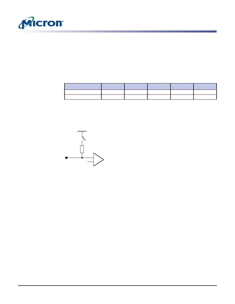
Programmable Impedance Output Buffer
The RLDRAM II is equipped with programmable impedance output buffers. This allows
a user to match the driver impedance to the system. To adjust the impedance, an exter-
nal precision resistor (RQ) is connected between the ZQ ball and V
SS
. The value of the
resistor must be five times the desired impedance. For example, a 300 resistor is
required for an output impedance of 60. To ensure that output impedance is one fifth
the value of RQ (within 15 percent), the range of RQ is 125 to 300.
Output impedance updates may be required because, over time, variations may occur in
supply voltage and temperature. The device samples the value of RQ. An impedance
update is transparent to the system and does not affect device operation. All data sheet
timing and current specifications are met during an update.
Clock Considerations
The RLDRAM II utilizes internal delay-locked loops for maximum output, data valid
windows. It can be placed into a stopped-clock state to minimize power with a modest
restart time of 1,024 cycles.
Table 10:
Clock Input Operating Conditions
Notes 1≠8
Parameter/Condition
Symbol
Min
Max
Units
Notes
Clock Input Voltage Level; CK and CK#
V
IN
(
DC
)
-0.3
V
DD
Q + 0.3
V
Clock Input Differential Voltage; CK and CK#
V
ID
(
DC
)
0.2
V
DD
Q + 0.6
V
9
Clock Input Differential Voltage; CK and CK#
V
ID
(
AC
)
0.4
V
DD
Q + 0.6
V
9
Clock Input Crossing Point Voltage; CK and CK#
V
IX
(
AC
)
V
DD
Q/2 - 0.15
V
DD
Q/2 + 0.15
V
10
V
EXT
V
DD
V
DD
Q
V
REF
CK#
CK
CMD
200µs MIN
t
MRSC
t
RC
2,048
cycles
MIN
6 ◊ 2,048
cycles
MIN
MRS
MRS
MRS
RF0
RF1
RF7
AC
DON'T CARE
ADD
V
TT
NOP
NOP
NOP
PDF: 09005aef80a41b46/Source: 09005aef809f284b
Micron Technology, Inc., reserves the right to change products or specifications without notice.
MT49H8M36_2.fm - Rev. H 8/05 EN
16
©2002 Micron Technology, Inc. All rights reserved.
288Mb: x36, x18, x9 2.5V V
EXT
, 1.8V V
DD
, HSTL, RLDRAM II
Clock Considerations
Figure 5:
Clock Input
Notes: 1. DKx and DKx# have the same requirements as CK and CK#.
2. All voltages referenced to V
SS
.
3. Tests for AC timing, I
DD
, and electrical AC and DC characteristics may be conducted at
nominal reference/supply voltage levels, but the related specifications and device opera-
tions are tested for the full voltage range specified.
4. Outputs (except for I
DD
measurements) measured with equivalent load.
5. AC timing and I
DD
tests may use a V
IL
-to-V
IH
swing of up to 1.5V in the test environment,
but input timing is still referenced to V
REF
(or to the crossing point for CK/CK#), and
parameter specifications are tested for the specified AC input levels under normal use con-
ditions. The minimum slew rate for the input signals used to test the device is 2 V/ns in the
range between V
IL
(
AC
) and V
IH
(
AC
).
6. The AC and DC input level specifications are as defined in the HSTL Standard (i.e., the
receiver will effectively switch as a result of the signal crossing the AC input level, and will
remain in that state as long as the signal does not ring back above [below] the DC input
LOW [HIGH] level).
7. The CK/CK# input reference level (for timing referenced to CK/CK#) is the point at which
CK and CK# cross. The input reference level for signals other than CK/CK# is V
REF
.
8. CK and CK# input slew rate must be
2 V/ns (4 V/ns if measured differentially).
9. V
ID
is the magnitude of the difference between the input level on CK and the input level
on CK#.
10. The value of V
IX
is expected to equal V
DD
Q/2 of the transmitting device and must track
variations in the DC level of the same.
11. CK and CK# must cross within this region.
12. CK and CK# must meet at least V
ID
(
DC
) MIN when static and centered around V
DD
Q/2.
13. Minimum peak-to-peak swing.
CK
CK#
V
IN
(
DC
) MAX
11
12
Maximum Clock Level
Minimum Clock Level
13
V
IN
(
DC
) MIN
V
DD
Q/2
V
DD
Q/2 + 0.15
V
DD
Q/2 - 0.15
X
X
V
ID
(
AC
)
V
ID
(
DC
)
V
IX
(
AC
) MAX
V
IX
(
AC
) MIN
PDF: 09005aef80a41b46/Source: 09005aef809f284b
Micron Technology, Inc., reserves the right to change products or specifications without notice.
MT49H8M36_2.fm - Rev. H 8/05 EN
17
©2002 Micron Technology, Inc. All rights reserved.
288Mb: x36, x18, x9 2.5V V
EXT
, 1.8V V
DD
, HSTL, RLDRAM II
Mode Register Set Command (MRS)
Mode Register Set Command (MRS)
The mode register stores the data for controlling the operating modes of the memory. It
programs the RLDRAM configuration, burst length, test mode, and I/O options. During
a MRS command, the address inputs A(17:0) are sampled and stored in the mode regis-
ter.
t
MRSC must be met before any command can be issued to the RLDRAM. The mode
register may be set at any time during device operation. However, any pending opera-
tions are not guaranteed to successfully complete. See the RLDRAM II design guide for
more details.
Figure 6:
Mode Register Set Timing
Note:
MRS: MRS command; AC: any command.
Figure 7:
Mode Register Set
Note:
COD: code to be loaded into the register.
CK#
CK
CMD
t
MRSC
MRS
NOP
NOP
AC
DON'T CARE
CK#
CK
WE#
REF#
A(17:0)
CS#
COD
A(20:18)
BA(2:0)
PDF: 09005aef80a41b46/Source: 09005aef809f284b
Micron Technology, Inc., reserves the right to change products or specifications without notice.
MT49H8M36_2.fm - Rev. H 8/05 EN
18
©2002 Micron Technology, Inc. All rights reserved.
288Mb: x36, x18, x9 2.5V V
EXT
, 1.8V V
DD
, HSTL, RLDRAM II
Configuration Table
Figure 8:
Mode Register Bit Map
Notes: 1. Bits A(17:10) must be set to zero.
2. BL = 8 is not available for configuration 1.
3. ±15% temperature variation.
Configuration Table
Table 11 shows, for different operating frequencies, the different RLDRAM configura-
tions that can be programmed into the mode register. The READ and WRITE latency
(
t
RL and
t
WL) values along with the row cycle times (
t
RC) are shown in clock cycles as
well as in nanoseconds. The shaded areas correspond to configurations that are not
allowed.
Notes: 1. BL = 8 is not available for configuration 1.
Table 11:
RLDRAM Configuration Table
Frequency
Symbol
Configuration
Units
1
1
2
3
t
RC
4
6
8
cycles
t
RL
4
6
8
cycles
t
WL
5
7
9
cycles
400 MHz
t
RC
20.0
ns
t
RL
20.0
ns
t
WL
22.5
ns
300 MHz
t
RC
20.0
26.7
ns
t
RL
20.0
26.7
ns
t
WL
23.3
30.0
ns
200 MHz
t
RC
20.0
30.0 40.0
ns
t
RL
20.0
30.0
40.0
ns
t
WL
25.0
35.0
45.0
ns
A2
A4
A5
A(17:10)
A3
A1
A0
A6
A7
A3
0
1
BL
4
A4
0
1
8
2
0
0
1
1
Reserved1
A9
A7
0
1
A8
A2
A1
A0
1
0
Configuration
Configuration
RLDRAM
Configuration
1
2
(default)
Reserved
Reserved
Reserved
1
2
Not valid
2 (default)
DLL enabled
DLL Reset
DLL Reset
Burst Length
Burst Length
DLL Reset
Address
Mux
Address Mux
DLL reset (default)
2
3
Reserved
1
0
1
1
0
1
0
1
0
0
0
0
1
1
0
0
1
0
1
0
1
1
Impedance
Matching
Impedance
Matching
A8
0
1
Resistor
External
Internal 50
3
(default)
A5
0
1
Nonmultiplexed
(default)
Address multiplexed
Address Mux
A9
0
1
Enabled
Termination
On-Die
Termination
Disabled (default)
On-Die
Termination
Unused

PDF: 09005aef80a41b46/Source: 09005aef809f284b
Micron Technology, Inc., reserves the right to change products or specifications without notice.
MT49H8M36_2.fm - Rev. H 8/05 EN
19
©2002 Micron Technology, Inc. All rights reserved.
288Mb: x36, x18, x9 2.5V V
EXT
, 1.8V V
DD
, HSTL, RLDRAM II
Write Basic Information
Write Basic Information
Write accesses are initiated with a WRITE command, as shown in Figure 9. Row and
bank addresses are provided together with the WRITE command.
During WRITE commands, data will be registered at both edges of DK according to the
programmed burst length (BL). A WRITE latency (WL) one cycle longer than the pro-
grammed READ latency (RL + 1) is present, with the first valid data registered at the first
rising DK edge WL cycles after the WRITE command.
Any WRITE burst may be followed by a subsequent READ command. Figures 13 and 14
illustrate the timing requirements for a WRITE followed by a READ for bursts of two and
four, respectively.
Setup and hold times for incoming DQ relative to the DK edges are specified as
t
DS and
t
DH. The input data is masked if the corresponding DM signal is HIGH. The setup and
hold times for data mask are also
t
DS and
t
DH.
Figure 9:
WRITE Command
Note:
A: Address; BA: Bank address.
CK#
CK
WE#
REF#
CS#
A
A(20:0)
BA(2:0)
BA
DON'T CARE
PDF: 09005aef80a41b46/Source: 09005aef809f284b
Micron Technology, Inc., reserves the right to change products or specifications without notice.
MT49H8M36_2.fm - Rev. H 8/05 EN
20
©2002 Micron Technology, Inc. All rights reserved.
288Mb: x36, x18, x9 2.5V V
EXT
, 1.8V V
DD
, HSTL, RLDRAM II
Write Basic Information
Figure 10: Basic WRITE Burst/DM Timing
Figure 11: WRITE Burst Basic Sequence: BL = 2, RL = 4, WL = 5, Configuration 1
DQ
DM
t
DH
t
DS
D0
D1
D2
D3
DKx#
DKx
t
DH
t
DS
t
DH
t
DS
DON'T CARE
Write
Latency
Data
masked
Data
masked
CK#
CK
t
CKDK
CK#
CK
CMD
0
1
2
3
4
5
6
7
8
ADDR
WL = 5
D
D0a
D1a
D0b
D1b D2a D2b D3a
D3
WR
A
BA0
A
BA1
A
BA2
A
BA3
A
BA0
A
BA4
A
BA5
A
BA6
A
BA7
WR
WR
WR
WR
WR
WR
WR
WR
DK#
DK
RC = 4
DON'T CARE

PDF: 09005aef80a41b46/Source: 09005aef809f284b
Micron Technology, Inc., reserves the right to change products or specifications without notice.
MT49H8M36_2.fm - Rev. H 8/05 EN
21
©2002 Micron Technology, Inc. All rights reserved.
288Mb: x36, x18, x9 2.5V V
EXT
, 1.8V V
DD
, HSTL, RLDRAM II
Write Basic Information
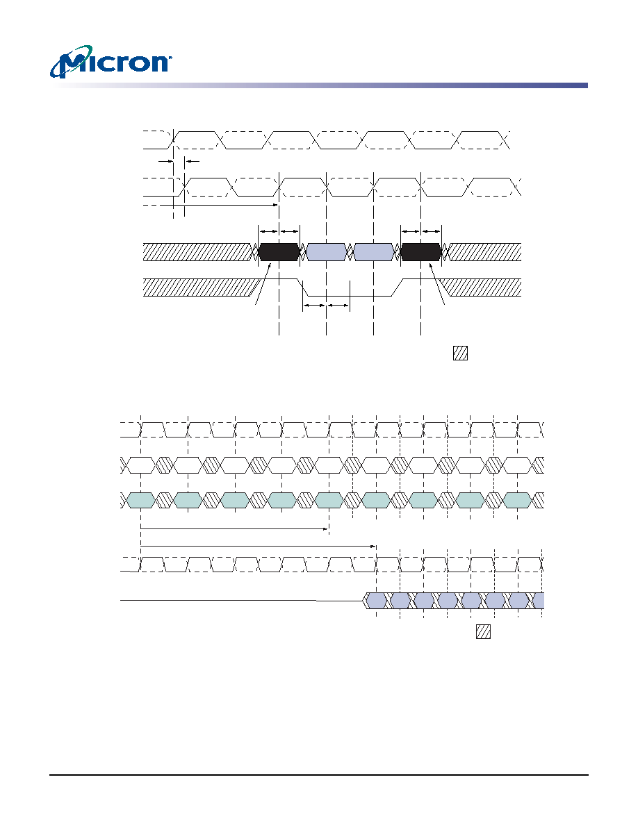
Figure 12: WRITE Burst Basic Sequence: BL = 4, RL = 4, WL = 5, Configuration 1
Notes: 1. A/BAx: Address A of bank x
WR: WRITE command
Dxy: Data y to bank x
RC: Row cycle time
WL: WRITE latency.
2. Any free bank may be used in any given CMD. The sequence shown is only one example of
a bank sequence.
Figure 13: WRITE Followed By READ: BL = 2, RL = 4, WL = 5, Configuration 1
ADDR
A
BA0
A
BA1
A
BA0
A
BA3
A
BA0
CK#
CK
CMD
0
1
2
3
4
5
6
7
8
WL = 5
D
D0a
D0c
D0b
D0d D1a D1b
D1c
D1
WR
NOP
WR
NOP
WR
NOP
WR
NOP
WR
DON'T CARE
DK#
DK
RC = 4
UNDEFINED
CK#
CK
CMD
0
1
2
3
4
5
6
7
8
9
ADDR
WL = 5
RL = 4
DQ
Q1a
Q2a
Q1b
Q2b
D0a
D0b
WR
A
BA0
A
BA1
A
BA2
NOP
RD
RD
NOP
NOP
NOP
NOP
NOP
NOP
DON'T CARE
QKx
QKx#
DKx#
DKx
QVLD
PDF: 09005aef80a41b46/Source: 09005aef809f284b
Micron Technology, Inc., reserves the right to change products or specifications without notice.
MT49H8M36_2.fm - Rev. H 8/05 EN
22
©2002 Micron Technology, Inc. All rights reserved.
288Mb: x36, x18, x9 2.5V V
EXT
, 1.8V V
DD
, HSTL, RLDRAM II
Read Basic Information
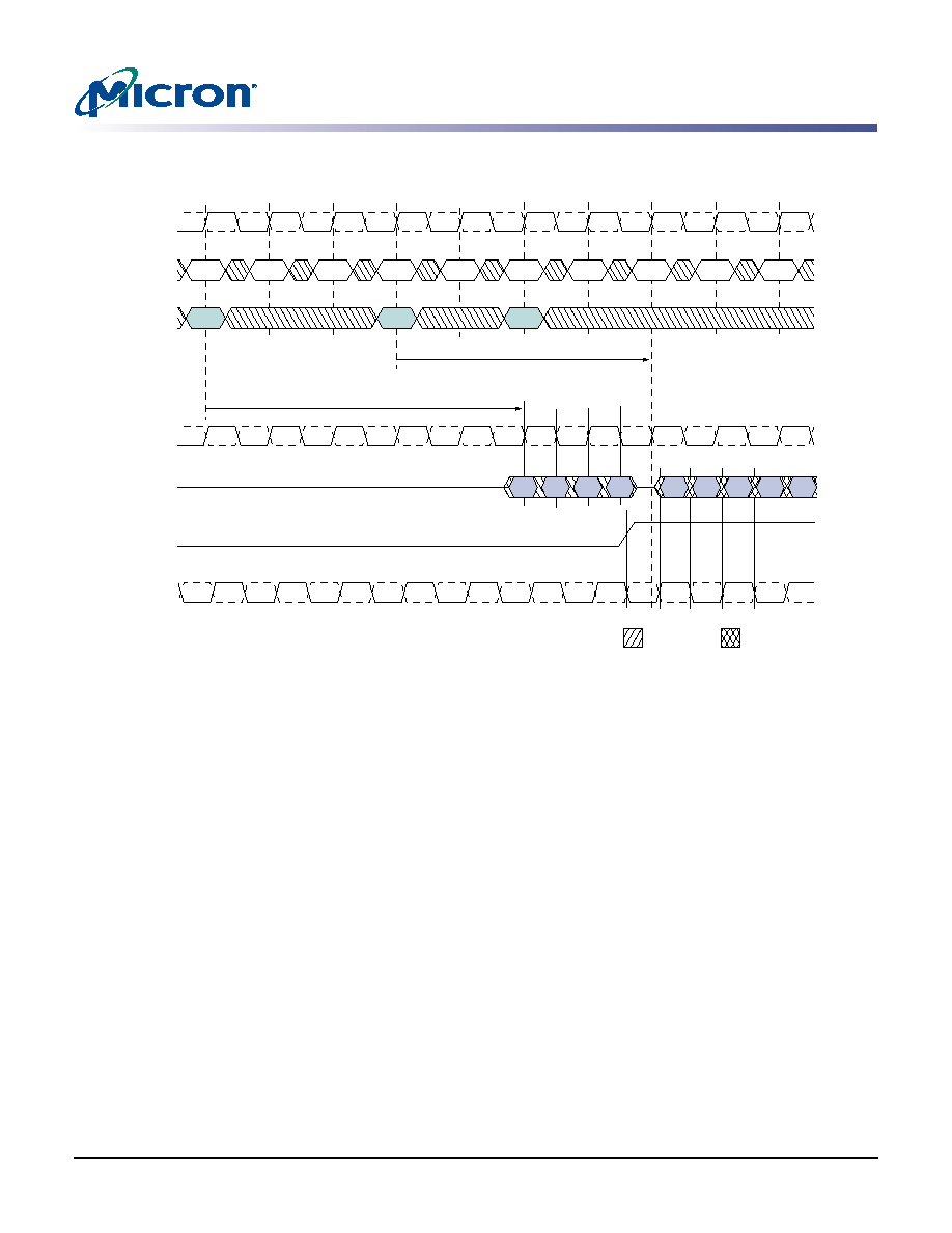
Figure 14: WRITE Followed By READ: BL = 4, RL = 4, WL = 5, Configuration 1
Note:
A/BAx: Address A of bank x
WR: WRITE
Dxy: Data y to bank x
WL: WRITE latency
RD: READ
Qxy: Data y from bank x
RL: READ latency.
Read Basic Information
Read accesses are initiated with a READ command, as shown in Figure 15. Row and
bank addresses are provided with the READ command.
During READ bursts, the memory device drives the read data edge-aligned with the QK
signal. After a programmable READ latency, data is available at the outputs. The data
valid signal indicates that valid data will be present in the next half clock cycle.
The skew between QK and the crossing point of CK is specified as
t
CKQK.
t
QKQ0 is the
skew between QK0 and the last valid data edge considered over all the data generated at
the DQ signals.
t
QKQ1 is the skew between QK1 and the last valid data edge considered
over all the data generated at the DQ signals.
t
QKQx is derived at each QKx clock edge
and is not cumulative over time.
t
QKQ is the maximum of
t
QKQ0 and
t
QKQ1.
After completion of a burst, assuming no other commands have been initiated, output
data (DQ) will go High-Z. Back-to-back READ commands are possible, producing a con-
tinuous flow of output data.
The data valid window is derived from each QK transisition and is defined as:
MIN (
t
QKH,
t
QKL) - 2(
t
QKQ [MAX]).
UNDEFINED
CK#
CK
CMD
0
1
2
3
4
5
6
7
8
9
ADDR
WL = 5
RL = 4
DQ
Q1a
Q1c
Q1b
Q1d
Q2a
D0a
D0b
D0c
D0d
WR
A
BA0
A
BA1
A
BA2
NOP
NOP
RD
NOP
RD
NOP
NOP
NOP
NOP
QKx
QKx#
DKx#
DKx
DON'T CARE
QVLD
PDF: 09005aef80a41b46/Source: 09005aef809f284b
Micron Technology, Inc., reserves the right to change products or specifications without notice.
MT49H8M36_2.fm - Rev. H 8/05 EN
23
©2002 Micron Technology, Inc. All rights reserved.
288Mb: x36, x18, x9 2.5V V
EXT
, 1.8V V
DD
, HSTL, RLDRAM II
Read Basic Information
Any READ burst may be followed by a subsequent WRITE command. Figures 19 and 20
illustrate the timing requirements for a READ followed by a WRITE. Depending on the
programmed READ latency, a READ-to-WRITE delay occurs in order to prevent bus con-
tention. Some systems having long line lengths or severe skews may need additional idle
cycles inserted. Refer to the RLDRAM II design guide for more details.
Figure 15: READ Command
Note:
A: Address; BA: Bank address.
Figure 16: Basic READ Burst Timing
Notes: 1. Minimum data valid window can be expressed as MIN (
t
QKH,
t
QKL) - 2 x
t
QKQx (MAX).
2.
t
QKQ0 is referenced to DQ0≠DQ17 in x36 and DQ0≠DQ8 in x18.
t
QKQ1 is referenced to DQ18≠DQ35 in x36 and DQ9≠DQ17 in x18.
3.
t
QKQ takes into account the skew between any QKx and any DQ.
CK#
CK
WE#
REF#
CS#
A
BA
A(20:0)
BA(2:0)
DON'T CARE
UNDEFINED
t
QKVLD
t
QKVLD
t
QKQ
Note 1
t
QKQ
t
QKQ
t
CKQK
QVLD
DQ
CK#
CK
QKx
QKx#
t
CKH
t
CKL
t
CK
Q0
Q1
Q2
Q3
t
QKL
t
QKH
PDF: 09005aef80a41b46/Source: 09005aef809f284b
Micron Technology, Inc., reserves the right to change products or specifications without notice.
MT49H8M36_2.fm - Rev. H 8/05 EN
24
©2002 Micron Technology, Inc. All rights reserved.
288Mb: x36, x18, x9 2.5V V
EXT
, 1.8V V
DD
, HSTL, RLDRAM II
Read Basic Information
Figure 17: READ Burst: BL = 2, RL = 4, Configuration 1
Figure 18: READ Burst: BL = 4, RL = 4, Configuration 1
Note:
A/BAx: Address A of bank x
RD: READ
Dxy: Data y to bank x
RC: Row cycle time
RL: READ latency.
CK#
CK
CMD
0
1
2
3
4
5
6
7
8
ADDR
RC = RL = 4
DQ
QKx
QKx#
Q0a
Q1a
Q0b
Q1b Q2a Q2b Q3a Q3b Q0a
RD
A
BA0
A
BA1
A
BA2
A
BA3
A
BA0
A
BA7
A
BA6
A
BA5
A
BA4
RD
RD
RD
RD
RD
RD
RD
RD
DON'T CARE
UNDEFINED
QVLD
CK#
CK
CMD
0
1
2
3
4
5
6
7
8
ADDR
RC = RL = 4
DQ
QKx
QKx#
Q0a
Q0c
Q0b
Q0d Q1a Q1b Q1c
Q1d Q0a
RD
A
BA0
A
BA1
A
BA0
A
BA1
A
BA3
NOP
RD
NOP
RD
NOP
RD
NOP
RD
DON'T CARE
UNDEFINED
QVLD

PDF: 09005aef80a41b46/Source: 09005aef809f284b
Micron Technology, Inc., reserves the right to change products or specifications without notice.
MT49H8M36_2.fm - Rev. H 8/05 EN
25
©2002 Micron Technology, Inc. All rights reserved.
288Mb: x36, x18, x9 2.5V V
EXT
, 1.8V V
DD
, HSTL, RLDRAM II
Read Basic Information
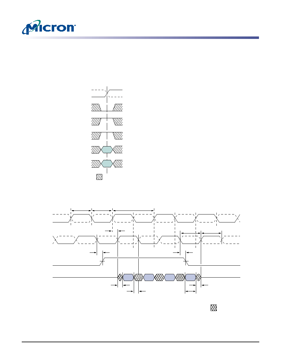
Figure 19: READ followed by WRITE, BL = 2, RL = 4, WL = 5, Configuration 1
Figure 20: READ followed by WRITE, BL = 4, RL = 4, WL = 5, Configuration 1
Note:
A/BAx: Address A of bank x
WR: WRITE command
Dxy: data y to bank x
WL: Write latency
RD: READ command
Qxy: Data y from bank x
RL: READ latency.
Q0a Q0b
CK#
CK
CMD
0
1
2
3
4
5
6
7
8
ADDR
RL = 4
DQ
QKx
QKx#
D1a D1b
RD
A
BA0
A
BA1
WR
WR
NOP
NOP
NOP
NOP
NOP
NOP
DON'T CARE
UNDEFINED
9
A
BA2
WL = 5
DKx#
DKx
D2a D2b
QVLD
Q0a
CK#
CK
CMD
0
1
2
3
4
5
6
7
ADDR
RL = 4
QKx
QKx#
RD
A
BA0
A
BA1
NOP
WR
NOP
NOP
NOP
NOP
NOP
DON'T CARE
WL = 5
DQ
D1a
D1b
Q0c
Q0b
Q0d
DKx#
DKx
UNDEFINED
QVLD
PDF: 09005aef80a41b46/Source: 09005aef809f284b
Micron Technology, Inc., reserves the right to change products or specifications without notice.
MT49H8M36_2.fm - Rev. H 8/05 EN
26
©2002 Micron Technology, Inc. All rights reserved.
288Mb: x36, x18, x9 2.5V V
EXT
, 1.8V V
DD
, HSTL, RLDRAM II
AUTO REFRESH Command (AREF)
AUTO REFRESH Command (AREF)
AREF is used to perform a REFRESH cycle on one row in a specific bank. The row
addresses are generated by an internal refresh counter for each bank; external address
balls are "Don't Care." The delay between the AREF command and a subsequent com-
mand to the same bank must be at least
t
RC.
Within a period of 32ms (
t
REF), the entire memory must be refreshed. Figure 22 illus-
trates an example of a continuous refresh sequence. Other refresh strategies, such as
burst refresh, are also possible.
Figure 21: AUTO REFRESH Command
Note:
BA: Bank address.
Figure 22: AUTO REFRESH Cycle
Notes: 1. ACx: Any command on bank x
ARFx: Auto refresh bank x
ACy: Any command on different bank.
2.
t
RC is configuration-dependent. Refer to Table 11 on page 18.
CK#
CK
WE#
REF#
CS#
A(20:0)
BA(2:0)
BA
DON'T CARE
CK#
CK
CMD
t
RC
ARFx
ACy
ACx
ACy
ARFx
ACy
DON'T CARE
PDF: 09005aef80a41b46/Source: 09005aef809f284b
Micron Technology, Inc., reserves the right to change products or specifications without notice.
MT49H8M36_2.fm - Rev. H 8/05 EN
27
©2002 Micron Technology, Inc. All rights reserved.
288Mb: x36, x18, x9 2.5V V
EXT
, 1.8V V
DD
, HSTL, RLDRAM II
On-Die Termination
On-Die Termination
On-die termination (ODT) is enabled by setting A9 to "1" during a MRS command. With
ODT on, all the DQs and DM are terminated to V
TT
with a resistance R
TT
. The command,
address, and clock signals are not terminated. Figure 23 below shows the equivalent cir-
cuit of a DQ receiver with ODT. ODTs are dynamically switched off during READ com-
mands and are designed to be off prior to the RLDRAM driving the bus. Similarly, ODTs
are designed to switch on after the RLDRAM has issued the last piece of data.
Notes: 1. All voltages referenced to V
SS
(GND).
2. V
TT
is expected to be set equal to V
REF
and must track variations in the DC level of V
REF
.
3. The R
TT
value is measured at 70∞C T
C
.
Figure 23: On-Die Termination-Equivalent Circuit
Table 12:
On-Die Termination DC Parameters
Description
Symbol
Min
Max
Units
Notes
Termination Voltage
V
TT
0.95
X
V
REF
1.05
X
V
REF
V
1, 2
On-Die Termination
R
TT
135
165
3
V
TT
R
TT
sw
Receiver
DQ

PDF: 09005aef80a41b46/Source: 09005aef809f284b
Micron Technology, Inc., reserves the right to change products or specifications without notice.
MT49H8M36_2.fm - Rev. H 8/05 EN
28
©2002 Micron Technology, Inc. All rights reserved.
288Mb: x36, x18, x9 2.5V V
EXT
, 1.8V V
DD
, HSTL, RLDRAM II
On-Die Termination
Figure 24: READ Burst with ODT: BL = 2, Configuration 1
Note:
A/BAx: address A of bank x
RD: READ
Qxy: Data y to bank x
RL: READ latency.
Figure 25: READ NOP READ with ODT: BL = 2, Configuration 1
CK#
CK
CMD
0
1
2
3
4
5
6
7
8
ADDR
RL = 4
DQ
QKx
QKx#
Q0a
Q1a
Q0b
Q1b Q2a Q2b
RD
A
BA0
A
BA1
A
BA2
RD
RD
NOP
NOP
NOP
NOP
NOP
NOP
DON'T CARE
UNDEFINED
ODT
ODT ON
QVLD
ODT OFF
ODT ON
CK#
CK
CMD
0
1
2
3
4
5
6
7
8
ADDR
RL = 4
DQ
QKx
QKx#
Q0a Q0b
Q2a Q2b
RD
A
BA0
A
BA2
NOP
RD
NOP
NOP
NOP
NOP
NOP
NOP
DON'T CARE
UNDEFINED
ODT
ODT ON
QVLD
ODT ON
ODT OFF
ODT OFF
ODT ON

PDF: 09005aef80a41b46/Source: 09005aef809f284b
Micron Technology, Inc., reserves the right to change products or specifications without notice.
MT49H8M36_2.fm - Rev. H 8/05 EN
29
©2002 Micron Technology, Inc. All rights reserved.
288Mb: x36, x18, x9 2.5V V
EXT
, 1.8V V
DD
, HSTL, RLDRAM II
On-Die Termination
Figure 26: READ NOP NOP READ with ODT: BL = 2, Configuration 1
Note:
A/BAx: address A of bank x
RD: READ
Qxy:Data y to bank x
RL: READ latency.
Figure 27: READ followed by WRITE with ODT: BL = 2, Configuration 1
CK#
CK
CMD
0
1
2
3
4
5
6
7
8
ADDR
RL = 4
DQ
QKx
QKx#
Q0a Q0b
Q2a Q2b
RD
A
BA0
A
BA2
NOP
NOP
RD
NOP
NOP
NOP
NOP
NOP
DON'T CARE
UNDEFINED
ODT
ODT ON
QVLD
ODT ON
ODT OFF
ODT OFF
ODT ON
9
CK#
CK
CMD
0
1
2
3
4
5
6
7
8
ADDR
RL = 4
DQ
QKx
QKx#
Q0a Q0b
D1a D1b
RD
A
BA0
A
BA1
WR
WR
NOP
NOP
NOP
NOP
NOP
NOP
DON'T CARE
UNDEFINED
ODT
ODT ON
ODT ON
ODT OFF
9
A
BA2
WL = 5
DKx#
DKx
D2a D2b
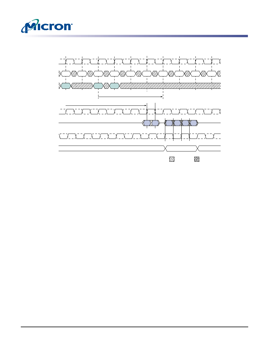
PDF: 09005aef80a41b46/Source: 09005aef809f284b
Micron Technology, Inc., reserves the right to change products or specifications without notice.
MT49H8M36_2.fm - Rev. H 8/05 EN
30
©2002 Micron Technology, Inc. All rights reserved.
288Mb: x36, x18, x9 2.5V V
EXT
, 1.8V V
DD
, HSTL, RLDRAM II
Operation with Multiplexed Addresses
Figure 28: WRITE followed by READ with ODT: BL = 2, Configuration 1
Note:
A/BAx: Address A of bank x
WR: WRITE command
Dxy: data y to bank x
WL: WRITE latency
RD: READ command
Qxy: Data y from bank x
RL: READ latency.
Operation with Multiplexed Addresses
In multiplexed address mode, the address can be provided to the RLDRAM in two parts
that are latched into the memory with two consecutive rising clock edges. This provides
the advantage that a maximim of 11 address balls are required to control the RLDRAM,
reducing the number of balls on the controller side. The data bus efficiency in continu-
ous burst mode is not affected for BL = 4 and BL = 8 since at least two clocks are required
to read the data out of the memory. The bank addresses are delivered to the RLDRAM at
the same time as the write command and the first address part, Ax.
This option is available by setting bit A5 to "1" in the mode register. Once this bit is set,
the READ, WRITE, and MRS commands follow the format described in Figure 29. See
Figure 31 on page 32 for the power-up sequence.
UNDEFINED
CK#
CK
CMD
0
1
2
3
4
5
6
7
8
9
ADDR
WL = 5
RL = 4
DQ
Q1a
Q2a
Q1b
Q2b
D0a
D0b
WR
A
BA0
A
BA1
A
BA2
NOP
RD
RD
NOP
NOP
NOP
NOP
NOP
NOP
DON'T CARE
QKx
QKx#
DKx#
DKx
ODT
ODT ON
ODT ON
ODT OFF
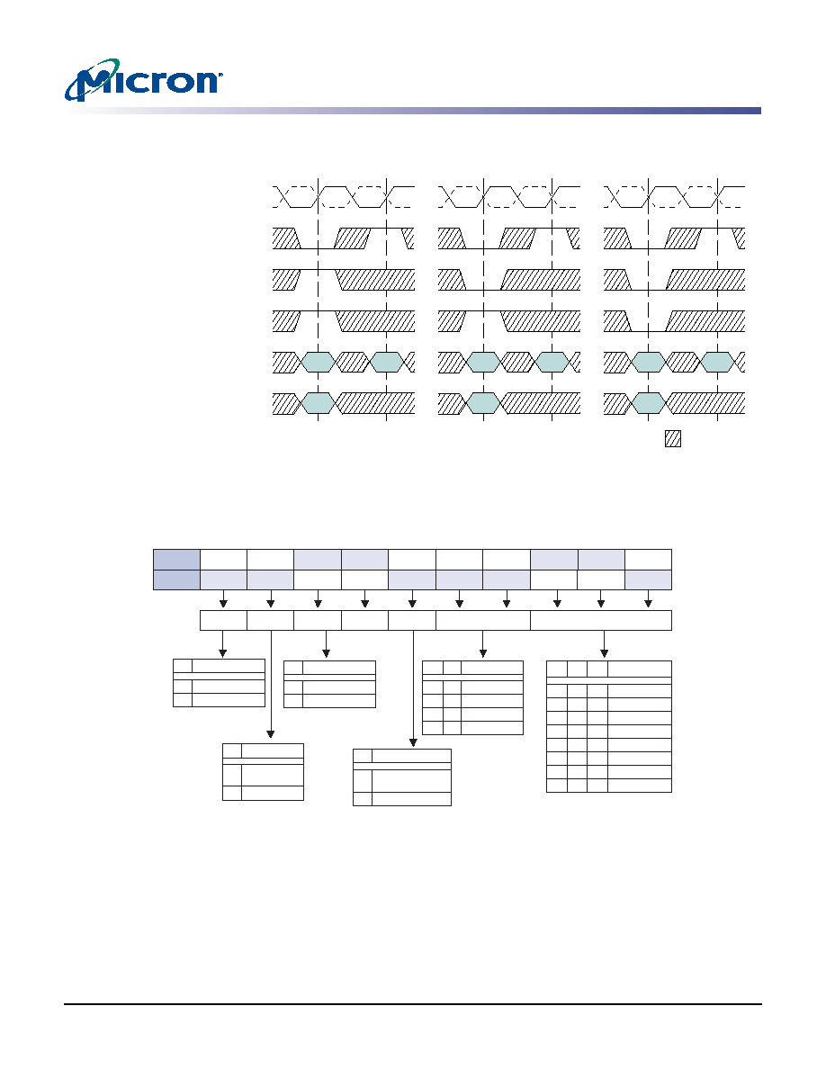
PDF: 09005aef80a41b46/Source: 09005aef809f284b
Micron Technology, Inc., reserves the right to change products or specifications without notice.
MT49H8M36_2.fm - Rev. H 8/05 EN
31
©2002 Micron Technology, Inc. All rights reserved.
288Mb: x36, x18, x9 2.5V V
EXT
, 1.8V V
DD
, HSTL, RLDRAM II
Operation with Multiplexed Addresses
Figure 29: Command Description in Multiplexed Address Mode
Notes: 1. Ax, Ay: Address
BA: Bank Address.
2. The minimum setup and hold times of the two address parts are defined
t
AS and
t
AH.
Figure 30: Mode Register Set Command in Multiplexed Address Mode
Notes: 1. The addresses A0, A3, A4, A5, A8, and A9 must be set as follows in order to activate the
mode register in the multiplexed address mode
2. Bits A(17:10) must be set to zero.
3. BL = 8 is not available for configuration 1.
4. ±15% temperature variation.
CK#
CK
WE#
REF#
CS#
Ax
BA
A<20:0>
BA<2:0>
READ
Ay
Ax
BA
WRITE
Ay
Ax
BA
DON'T CARE
MRS
Ay
A4
A5
A4
A3
A3
A0
A8
A9
A3x
0
1
BL
4
A4x
0
1
8
3
0
0
1
1
A9
A9y
0
1
A8
A4y A3y A0x
1
0
Configuration
Configuration
RLDRAM
Configuration
1
3
(default)
Reserved
Reserved
Reserved
1
3
Not valid
2 (default)
DLL enabled
DLL Reset
DLL Reset
Burst Length
Burst Length
DLL Reset
Address
Mux
Address Mux
DLL reset (default)
2
3
Reserved
1
0
1
1
0
1
0
1
0
0
0
0
1
1
0
0
1
0
1
0
1
1
Impedance
Matching
Impedance
Matching
A8x
0
1
Resistor
External
A5x
0
1
Nonmultiplexed
(default)
Address multiplexed
A9x
0
1
Enabled
Termination
Disabled (default)
On-Die
Termination
On-Die
Termination
Unused
Ax
Ay
Internal 50
4
(default)

PDF: 09005aef80a41b46/Source: 09005aef809f284b
Micron Technology, Inc., reserves the right to change products or specifications without notice.
MT49H8M36_2.fm - Rev. H 8/05 EN
32
©2002 Micron Technology, Inc. All rights reserved.
288Mb: x36, x18, x9 2.5V V
EXT
, 1.8V V
DD
, HSTL, RLDRAM II
Operation with Multiplexed Addresses
Figure 31: Power-Up Sequence in Multiplexed Address Mode
Notes: 1.
The above sequence must be respected in order to power up the RLDRAM in the
multiplexed address mode
.
2. MRS: MRS command
RFx: REFRESH Bank x
AC: any command.
3. Address A5 must be set HIGH (muxed address mode setting when RLDRAM is in normal
mode of operation).
4. Address A5 must be set HIGH (muxed address mode setting when RLDRAM is already in
muxed address mode).
V
EXT
V
DD
V
DD
Q
V
REF
CK#
CK
CMD
200µs MIN
t
MRSC
t
RC
2,048 cycles
MIN
6 ◊ 2,048
cycles MIN
MRS
MRS
MRS
RF0
RF1
RF7
AC
DON'T CARE
ADD
V
TT
A
3
MRS
Ax
4
Ay
t
MRSC
1 cycle
MIN
1 cycle
MIN
NOP
NOP
NOP
NOP

PDF: 09005aef80a41b46/Source: 09005aef809f284b
Micron Technology, Inc., reserves the right to change products or specifications without notice.
MT49H8M36_2.fm - Rev. H 8/05 EN
33
©2002 Micron Technology, Inc. All rights reserved.
288Mb: x36, x18, x9 2.5V V
EXT
, 1.8V V
DD
, HSTL, RLDRAM II
Address Mapping
Address Mapping
The address mapping is described in Table 13 as a function of data width and burst
length.
Notes: 1. X means "Don't Care."
2. Reserved for A20 expansion in multiplexed mode.
3. Reserved for A21 expansion in multiplexed mode.
Table 13:
Address Mapping in Multiplexed Address Mode
Note 1
Data
Width
Burst
Length
Ball
Address
A0
2
A3
A4
A5
3
A8
A9
A10
A13
A14
A17
A18
x36
BL = 2
Ax
A0
A3
A4
A5
A8
A9
A10
A13
A14
A17
A18
Ay
X
A1
A2
X
A6
A7
X
A11
A12
A16
A15
BL = 4
Ax
A0
A3
A4
A5
A8
A9
A10
A13
A14
A17
X
Ay
X
A1
A2
X
A6
A7
X
A11
A12
A16
A15
x18
BL = 2
Ax
A0
A3
A4
A5
A8
A9
A10
A13
A14
A17
A18
Ay
X
A1
A2
X
A6
A7
A19
A11
A12
A16
A15
BL = 4
Ax
A0
A3
A4
A5
A8
A9
A10
A13
A14
A17
A18
Ay
X
A1
A2
X
A6
A7
X
A11
A12
A16
A15
BL = 8
Ax
A0
A3
A4
A5
A8
A9
A10
A13
A14
A17
X
Ay
X
A1
A2
X
A6
A7
X
A11
A12
A16
A15
x9
BL = 2
Ax
A0
A3
A4
A5
A8
A9
A10
A13
A14
A17
A18
Ay
A20
A1
A2
X
A6
A7
A19
A11
A12
A16
A15
BL = 4
Ax
A0
A3
A4
A5
A8
A9
A10
A13
A14
A17
A18
Ay
X
A1
A2
X
A6
A7
A19
A11
A12
A16
A15
BL = 8
Ax
A0
A3
A4
A5
A8
A9
A10
A13
A14
A17
A18
Ay
X
A1
A2
X
A6
A7
X
A11
A12
A16
A15

PDF: 09005aef80a41b46/Source: 09005aef809f284b
Micron Technology, Inc., reserves the right to change products or specifications without notice.
MT49H8M36_2.fm - Rev. H 8/05 EN
34
©2002 Micron Technology, Inc. All rights reserved.
288Mb: x36, x18, x9 2.5V V
EXT
, 1.8V V
DD
, HSTL, RLDRAM II
Configuration Table
Configuration Table
In multiplexed address mode, the read and write latencies are increased by one clock
cycle. The RLDRAM cycle time remains the same, as described in Table 14.
Notes: 1. BL = 8 is not available for configuration 1.
REFRESH Command in Multiplexed Address Mode
Similar to other commands, the REFRESH command is executed on the next rising clock
edge when in the multiplexed address mode. However, since only bank address is
required for AREF, the next command can be applied on the following clock. The opera-
tion of the AREF command and any other command is represented in Figure 32.
Figure 32: Burst REFRESH Operation
Note:
AREF: AUTO REFRESH
AC: Any command
Ax: First part Ax of address
Ay: Second part Ay of address
BAk: Bank k; k is chosen so that
t
RC is met.
Table 14:
Configuration Table In Multiplexed Address Mode
Configuration
Frequency
Symbol
1
1
2
3
Unit
t
RC
4
6
8
cycles
t
RL
5
7
9
cycles
t
WL
6
8
10
cycles
400 MHz
t
RC
20.0
ns
t
RL
22.5
ns
t
WL
25.0
ns
300 MHz
t
RC
20.0
26.7
ns
t
RL
23.3
30.0
ns
t
WL
26.7
33.3
ns
200 MHz
t
RC
20.0
30.0 40.0
ns
t
RL
25.0
35.0
45.0
ns
t
WL
35.0
40.0
50.0
ns
ADDR
CK#
CK
CMD
0
1
2
3
4
5
6
7
8
AC
AREF
AREF
AREF
AREF
AREF
AREF
AREF
DON'T CARE
AREF
9
10
Ax
Ay
AC
Ax
Ay
11
BADDR
BAk
BA0
BA1
BA2
BA3
BA4
BA5
BA6
BA7
BAk
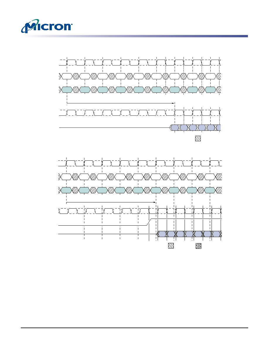
PDF: 09005aef80a41b46/Source: 09005aef809f284b
Micron Technology, Inc., reserves the right to change products or specifications without notice.
MT49H8M36_2.fm - Rev. H 8/05 EN
35
©2002 Micron Technology, Inc. All rights reserved.
288Mb: x36, x18, x9 2.5V V
EXT
, 1.8V V
DD
, HSTL, RLDRAM II
REFRESH Command in Multiplexed Address Mode
Figure 33: WRITE Burst Basic Sequence: BL = 4, with Multiplexed Addresses, Configuration 1,
WL = 6
Figure 34: READ Burst Basic Sequence: BL = 4, with Multiplexed Addresses, Configuration 1, RL = 5
Note:
Ax/BAk: Address Ax of bank k
Ay: Address Ay of bank k
WR: WRITE
Djk: Data k to bank j
WL: WRITE latency
Qjk: Data k to bank j
RD: READ
RL: READ latency.
CK#
CK
CMD
0
1
2
3
4
5
6
7
8
ADDR
WL = 6
DQ
D0a
D0c
D0b
D0d
D1a
D1
WR
Ax
BA0
Ay
Ax
BA1
Ay
Ax
BA2
Ay
Ax
BA3
Ay
Ax
BA0
NOP
WR
NOP
WR
NOP
WR
NOP
WR
DKx#
DKx
DON'T CARE
UNDEFINED
CK#
CK
CMD
0
1
2
3
4
5
6
7
8
ADDR
RL = 5
DQ
QKx
QKx#
Q0a
Q0c
Q0b
Q0d Q1a Q1b Q1c
RD
NOP
RD
NOP
RD
NOP
RD
NOP
RD
DON'T CARE
Ax
BA0
Ay
Ax
BA1
Ay
Ax
BA2
Ay
Ax
BA0
Ay
Ax
BA1
QVLD

PDF: 09005aef80a41b46/Source: 09005aef809f284b
Micron Technology, Inc., reserves the right to change products or specifications without notice.
MT49H8M36_2.fm - Rev. H 8/05 EN
36
©2002 Micron Technology, Inc. All rights reserved.
288Mb: x36, x18, x9 2.5V V
EXT
, 1.8V V
DD
, HSTL, RLDRAM II
IEEE 1149.1 Serial Boundary Scan (JTAG)
IEEE 1149.1 Serial Boundary Scan (JTAG)
RLDRAM incorporates a serial boundary scan test access port (TAP). This port operates
in accordance with IEEE Standard 1149.1-2001. The TAP operates using logic levels asso-
ciated with the V
DD
Q supply.
RLDRAM contains a TAP controller, instruction register, boundary scan register, bypass
register, and ID register.
Disabling the JTAG Feature
It is possible to operate RLDRAM without using the JTAG feature. To disable the TAP
controller, TCK must be tied LOW (V
SS
) to prevent clocking of the device. TDI and TMS
are internally pulled up and may be unconnected. They may alternately be connected to
V
DD
through a pull-up resistor. TDO should be left unconnected. Upon power-up, the
device will come up in a reset state, which will not interfere with the operation of the
device.
Test Access Port (TAP)
Test Clock (TCK)
The test clock is used only with the TAP controller. All inputs are captured on the rising
edge of TCK. All outputs are driven from the falling edge of TCK.
Test Mode Select (TMS)
The TMS input is used to give commands to the TAP controller and is sampled on the
rising edge of TCK. It is allowable to leave this ball unconnected if the TAP is not used.
The ball is pulled up internally, resulting in a logic HIGH level.
Test Data-In (TDI)
The TDI ball is used to serially input information into the registers and can be connected
to the input of any of the registers. The register between TDI and TDO is chosen by the
instruction that is loaded into the TAP instruction register. For information on loading
the instruction register, see Figure 35 on page 37. TDI is internally pulled up and can be
unconnected if the TAP is unused in an application. TDI is connected to the most signif-
icant bit (MSB) of any register (see Figure 36 on page 37).
Test Data-Out (TDO)
The TDO output ball is used to serially clock data-out from the registers. The output is
active depending upon the current state of the TAP state machine (see Figure 35). The
output changes on the falling edge of TCK. TDO is connected to the least significant bit
(LSB) of any register (see Figure 36).
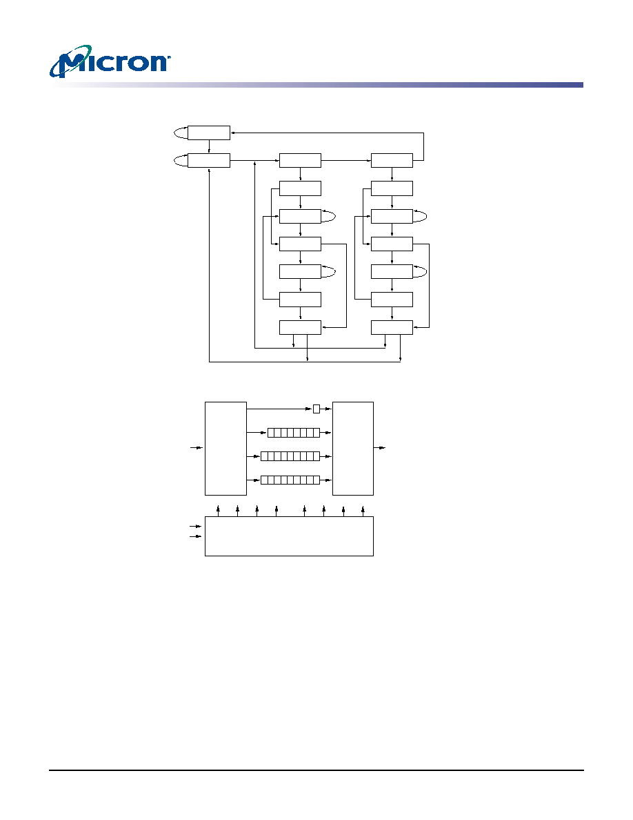
PDF: 09005aef80a41b46/Source: 09005aef809f284b
Micron Technology, Inc., reserves the right to change products or specifications without notice.
MT49H8M36_2.fm - Rev. H 8/05 EN
37
©2002 Micron Technology, Inc. All rights reserved.
288Mb: x36, x18, x9 2.5V V
EXT
, 1.8V V
DD
, HSTL, RLDRAM II
Test Access Port (TAP)
Figure 35: TAP Controller State Diagram
Figure 36: TAP Controller Block Diagram
Note:
x = 112 for all configurations.
Performing a TAP RESET
A reset is performed by forcing TMS HIGH (V
DD
Q) for five rising edges of TCK. This
RESET does not affect the operation of the RLDRAM and may be performed while the
RLDRAM is operating.
At power-up, the TAP is reset internally to ensure that TDO comes up in a High-Z state.
TAP Registers
Registers are connected between the TDI and TDO balls and allow data to be scanned
into and out of the RLDRAM test circuitry. Only one register can be selected at a time
through the instruction register. Data is serially loaded into the TDI ball on the rising
edge of TCK. Data is output on the TDO ball on the falling edge of TCK.
TEST-LOGIC
RESET
RUN-TEST/
IDLE
SELECT
DR-SCAN
SELECT
IR-SCAN
CAPTURE-DR
SHIFT-DR
CAPTURE-IR
SHIFT-IR
EXIT1-DR
PAUSE-DR
EXIT1-IR
PAUSE-IR
EXIT2-DR
UPDATE-DR
EXIT2-IR
UPDATE-IR
1
1
1
0
1
1
0
0
1
1
1
0
0
0
0
0
0
0
0
0
1
0
1
1
0
1
0
1
1
1
1
0
Bypass Register
0
Instruction Register
0
1
2
3
4
5
6
7
Identification Register
0
1
2
29
30
31
.
.
.
Boundary Scan Register
0
1
2
.
.
x
.
.
.
Selection
Circuitry
Selection
Circuitry
TCK
TMS
TAP Controller
TDI
TDO

PDF: 09005aef80a41b46/Source: 09005aef809f284b
Micron Technology, Inc., reserves the right to change products or specifications without notice.
MT49H8M36_2.fm - Rev. H 8/05 EN
38
©2002 Micron Technology, Inc. All rights reserved.
288Mb: x36, x18, x9 2.5V V
EXT
, 1.8V V
DD
, HSTL, RLDRAM II
TAP Instruction Set
Instruction Register
Eight-bit instructions can be serially loaded into the instruction register. This register is
loaded when it is placed between the TDI and TDO balls, as shown in Figure 36. Upon
power-up, the instruction register is loaded with the IDCODE instruction. It is also
loaded with the IDCODE instruction if the controller is placed in a reset state as
described in the previous section.
When the TAP controller is in the Capture-IR state, the two least significant bits are
loaded with a binary "01" pattern to allow for fault isolation of the board-level serial test
data path.
Bypass Register
To save time when serially shifting data through registers, it is sometimes advantageous
to skip certain chips. The bypass register is a single-bit register that can be placed
between the TDI and TDO balls. This allows data to be shifted through the RLDRAM
with minimal delay. The bypass register is set LOW (V
SS
) when the BYPASS instruction is
executed.
Boundary Scan Register
The boundary scan register is connected to all the input and bidirectional balls on the
RLDRAM. Several balls are also included in the scan register to reserved balls. The
RLDRAM has a 113-bit register.
The boundary scan register is loaded with the contents of the RAM I/O ring when the
TAP controller is in the Capture-DR state and is then placed between the TDI and TDO
balls when the controller is moved to the Shift-DR state.
The Boundary Scan Order tables (see Table 21 on page 43) show the order in which the
bits are connected. Each bit corresponds to one of the balls on the RLDRAM package.
The MSB of the register is connected to TDI, and the LSB is connected to TDO.
Identification (ID) Register
The ID register is loaded with a vendor-specific, 32-bit code during the Capture-DR state
when the IDCODE command is loaded in the instruction register. The IDCODE is hard-
wired into the RLDRAM and can be shifted out when the TAP controller is in the Shift-
DR state. The ID register has a vendor code and other information described in the Iden-
tification Register Definitions table on page 42.
TAP Instruction Set
Overview
Many different instructions (2
8
) are possible with the 8-bit instruction register. All used
combinations are listed in Table 20, Instruction Codes, on page 42. These six instruc-
tions are described in detail below. The remaining instructions are reserved and should
not be used.
The TAP controller used in this RLDRAM is fully compliant to the 1149.1 convention.
Instructions are loaded into the TAP controller during the Shift-IR state when the
instruction register is placed between TDI and TDO. During this state, instructions are
shifted through the instruction register through the TDI and TDO balls. To execute the
instruction once it is shifted in, the TAP controller needs to be moved into the Update-IR
state.

PDF: 09005aef80a41b46/Source: 09005aef809f284b
Micron Technology, Inc., reserves the right to change products or specifications without notice.
MT49H8M36_2.fm - Rev. H 8/05 EN
39
©2002 Micron Technology, Inc. All rights reserved.
288Mb: x36, x18, x9 2.5V V
EXT
, 1.8V V
DD
, HSTL, RLDRAM II
TAP Instruction Set
EXTEST
The EXTEST instruction allows circuitry external to the component package to be tested.
Boundary-scan register cells at output balls are used to apply a test vector, while those at
input balls capture test results. Typically, the first test vector to be applied using the
EXTEST instruction will be shifted into the boundary scan register using the PRELOAD
instrucion. Thus, during the Update-IR state of EXTEST, the output driver is turned on
and the PRELOAD data is driven onto the output balls.
IDCODE
The IDCODE instruction causes a vendor-specific, 32-bit code to be loaded into the
instruction register. It also places the instruction register between the TDI and TDO
balls and allows the IDCODE to be shifted out of the device when the TAP controller
enters the Shift-DR state. The IDCODE instruction is loaded into the instruction register
upon power-up or whenever the TAP controller is given a test logic reset state.
High-Z
The High-z instruction causes the boundary scan register to be connected between the
TDI and TDO. This places all RLDRAM outputs into a High-Z state.
CLAMP
When the CLAMP instruction is loaded into the instruction register, the data driven by
the output balls are determined from the values held in the boundary scan register.
SAMPLE/PRELOAD
When the SAMPLE/PRELOAD instruction is loaded into the instruction register and the
TAP controller is in the Capture-DR state, a snapshot of data on the inputs and bidirec-
tional balls is captured in the boundary scan register.
The user must be aware that the TAP controller clock can only operate at a frequency up
to 50 MHz, while the RLDRAM clock operates significantly faster. Because there is a large
difference between the clock frequencies, it is possible that during the Capture-DR state,
an input or output will undergo a transition. The TAP may then try to capture a signal
while in transition (metastable state). This will not harm the device, but there is no guar-
antee as to the value that will be captured. Repeatable results may not be possible.
To ensure that the boundary scan register will capture the correct value of a signal, the
RLDRAM signal must be stabilized long enough to meet the TAP controller's capture
setup plus hold time (tCS plus tCH). The RLDRAM clock input might not be captured
correctly if there is no way in a design to stop (or slow) the clock during a SAMPLE/PRE-
LOAD instruction. If this is an issue, it is still possible to capture all other signals and
simply ignore the value of the CK and CK# captured in the boundary scan register.
Once the data is captured, it is possible to shift out the data by putting the TAP into the
Shift-DR state. This places the boundary scan register between the TDI and TDO balls.
BYPASS
When the BYPASS instruction is loaded in the instruction register and the TAP is placed
in a Shift-DR state, the bypass register is placed between TDI and TDO. The advantage of
the BYPASS instruction is that it shortens the boundary scan path when multiple devices
are connected together on a board.
Reserved for Future Use
The remaining 22 instructions are not implemented but are reserved for future use. Do
not use these instructions.
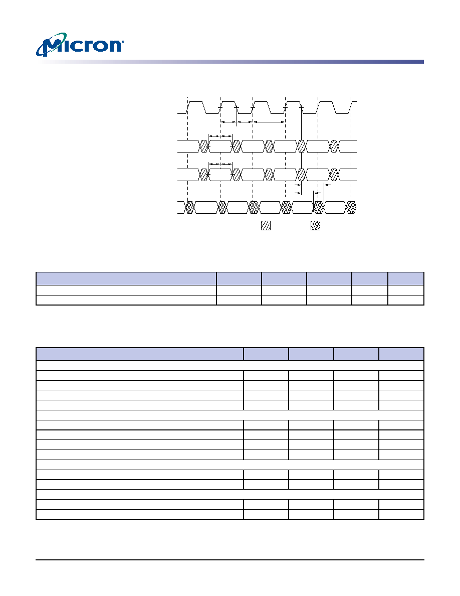
PDF: 09005aef80a41b46/Source: 09005aef809f284b
Micron Technology, Inc., reserves the right to change products or specifications without notice.
MT49H8M36_2.fm - Rev. H 8/05 EN
40
©2002 Micron Technology, Inc. All rights reserved.
288Mb: x36, x18, x9 2.5V V
EXT
, 1.8V V
DD
, HSTL, RLDRAM II
TAP Instruction Set
Figure 37: TAP Timing
Notes: 1.
t
CS and
t
CH refer to the setup and hold time requirements of latching data from the
boundary scan register.
Table 15:
TAP AC Electrical Characteristics and Operating Conditions
+0∞C
T
C
+95∞C; +1.7V V
DD
+1.9V, unless otherwise noted
Description
Symbol
Min
Max
Units
Notes
Input high (Logic 1) voltage
V
IH
V
REF
+ 0.3
V
DD
+ 0.3
V
1, 2
Input low (Logic 0) voltage
V
IL
V
SS
Q - 0.3
V
REF
- 0.3
V
1, 2
Table 16:
TAP AC Electrical Characteristics
Note 1; +0∞C
T
C
+95∞C; +1.7V V
DD
+1.9V
Description
Symbol
Min
Max
Units
Clock
Clock cycle time
t
THTH
20
ns
Clock frequency
f
TF
50
MHz
Clock HIGH time
t
THTL
10
ns
Clock LOW time
t
TLTH
10
ns
Output Times
TCK LOW to TDO unknown
t
TLOX
0
ns
TCK LOW to TDO valid
t
TLOV
10
ns
TDI valid to TCK HIGH
t
DVTH
5
ns
TCK HIGH to TDI invalid
t
THDX
5
ns
Setup Times
TMS setup
t
MVTH
5
ns
Capture setup
t
CS
5
ns
Hold Times
TMS hold
t
THMX
5
ns
Capture hold
t
CH
5
ns
t
TLTH
Test Clock
(TCK)
1
2
3
4
5
6
Test Mode Select
(TMS)
tTHTL
Test Data-Out
(TDO)
tTHTH
Test Data-In
(TDI)
tTHMX
tMVTH
tTHDX
tDVTH
tTLOX
tTLOV
DON'T CARE
UNDEFINED
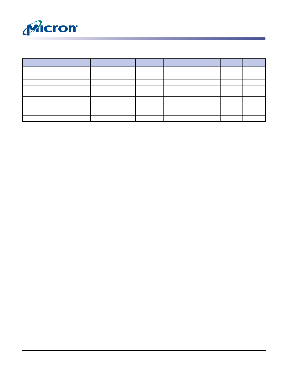
PDF: 09005aef80a41b46/Source: 09005aef809f284b
Micron Technology, Inc., reserves the right to change products or specifications without notice.
MT49H8M36_2.fm - Rev. H 8/05 EN
41
©2002 Micron Technology, Inc. All rights reserved.
288Mb: x36, x18, x9 2.5V V
EXT
, 1.8V V
DD
, HSTL, RLDRAM II
TAP Instruction Set
Notes: 1. All voltages referenced to V
SS
(GND).
2. Overshoot:
V
IH
(
AC
)
V
DD
+ 0.7V for t
t
CK/2.
Undershoot: V
IL
(
AC
)
-0.5V for t
t
CK/2.
During normal operation, V
DD
Q must not exceed V
DD
.
Table 17:
TAP DC Electrical Characteristics and Operating Conditions
+0∞C
T
C
+95∞C; +1.7V V
DD
+1.9V, unless otherwise noted
Description
Condition
Symbol
Min
Max
Units
Notes
Input high (Logic 1) voltage
V
IH
V
REF
+ 0.15
V
DD
+ 0.3
V
1, 2
Input low (Logic 0) voltage
V
IL
V
SS
Q - 0.3
V
REF
- 0.15
V
1, 2
Input leakage current
0V
V
IN
V
DD
IL
I
-5.0
5.0
µA
Output leakage current
Output disabled,
0V
V
IN
V
DD
Q
IL
O
-5.0
5.0
µA
Output low voltage
I
OLC
= 100µA
V
OL
1
0.2
V
1
Output low voltage
I
OLT
= 2mA
V
OL
2
0.4
V
1
Output high voltage
|I
OHC
| = 100µA
V
OH
1
V
DD
Q - 0.2
V
1
Output high voltage
|I
OHT
| = 2mA
V
OH
2
V
DD
Q - 0.4
V
1

PDF: 09005aef80a41b46/Source: 09005aef809f284b
Micron Technology, Inc., reserves the right to change products or specifications without notice.
MT49H8M36_2.fm - Rev. H 8/05 EN
42
©2002 Micron Technology, Inc. All rights reserved.
288Mb: x36, x18, x9 2.5V V
EXT
, 1.8V V
DD
, HSTL, RLDRAM II
TAP Instruction Set
Table 18:
Identification Register Definitions
Instruction Field
All Devices
Description
Revision Number
(31:28)
abcd
ab = die revision
cd = 10 for x36, 01 for x18, 00 for x9.
Device ID
(27:12)
00jkidef10100111
def = 000 for 288M, 001 for 576M, 010 for 1G.
i = 0 for common I/O, 1 for separate I/O.
jk = 00 for RLDRAM, 01 for RLDRAM II.
Micron JEDEC ID
Code (11:1)
00000101100
Allows unique identification of RLDRAM vendor.
ID Register Presence
Indicator (0)
1
Indicates the presence of an ID register.
Table 19:
Scan Register Sizes
Register Name
Bit Size
Instruction
8
Bypass
1
ID
32
Boundary Scan
113
Table 20:
Instruction Codes
Instruction
Code
Description
Extest
0000 0000
Captures I/O ring contents. Places the boundary scan register between TDI and TDO.
This operation does not affect RLDRAM operations.
ID Code
0010 0001
Loads the ID register with the vendor ID code and places the register between
TDI and TDO. This operation does not affect RLDRAM operations.
Sample/Preload
0000 0101
Captures I/O ring contents. Places the boundary scan register between TDI and TDO.
Clamp
0000 0111
Selects the bypass register to be connected between TDI and TDO. Data driven by
output balls are determined from values held in the boundary scan register.
High-Z
0000 0011
Selects the bypass register to be connected between TDI and TDO. All ouputs are forced
into high impedance state.
Bypass
1111 1111
Places the bypass register between TDI and TDO. This operation does not affect
RLDRAM operations.
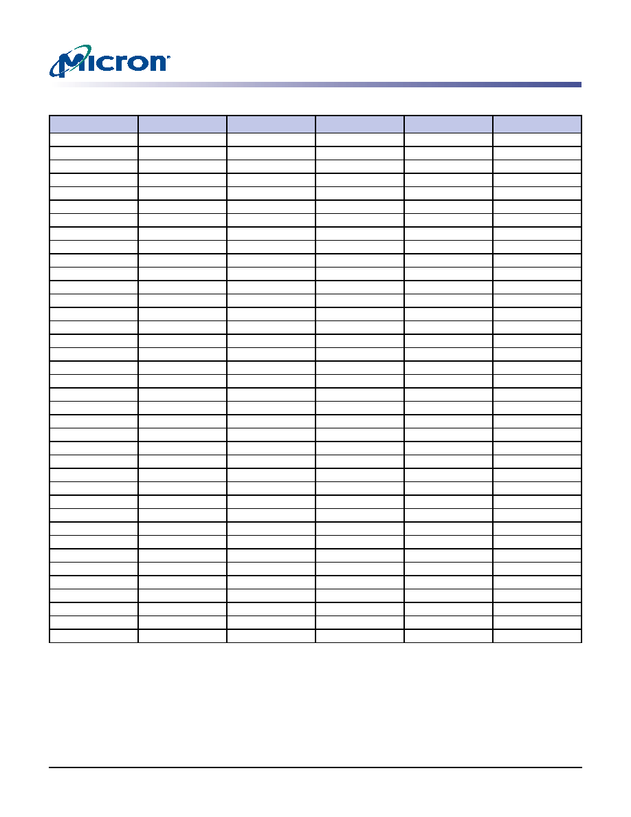
PDF: 09005aef80a41b46/Source: 09005aef809f284b
Micron Technology, Inc., reserves the right to change products or specifications without notice.
MT49H8M36_2.fm - Rev. H 8/05 EN
43
©2002 Micron Technology, Inc. All rights reserved.
288Mb: x36, x18, x9 2.5V V
EXT
, 1.8V V
DD
, HSTL, RLDRAM II
TAP Instruction Set
Notes: 1. Any unused balls that are in the order will read as a logic "0."
Table 21:
Boundary Scan (Exit) Order
Bit#
µBGA Ball
Bit#
µBGA Ball
Bit#
µBGA Ball
1
K1
39
R11
77
C11
2
K2
40
R11
78
C11
3
L2
41
P11
79
C10
4
L1
42
P11
80
C10
5
M1
43
P10
81
B11
6
M3
44
P10
82
B11
7
M2
45
N11
83
B10
8
N1
46
N11
84
B10
9
P1
47
N10
85
B3
10
N3
48
N10
86
B3
11
N3
49
P12
87
B2
12
N2
50
N12
88
B2
13
N2
51
M11
89
C3
14
P3
52
M10
90
C3
15
P3
53
M12
91
C2
16
P2
54
L12
92
C2
17
P2
55
L11
93
D3
18
R2
56
K11
94
D3
19
R3
57
K12
95
D2
20
T2
58
J12
96
D2
21
T2
59
J11
97
E2
22
T3
60
H11
98
E2
23
T3
61
H12
99
E3
24
U2
62
G12
100
E3
25
U2
63
G10
101
F2
26
U3
64
G11
102
F2
27
U3
65
E12
103
F3
28
V2
66
F12
104
F3
29
U10
67
F10
105
E1
30
U10
68
F10
106
F1
31
U11
69
F11
107
G2
32
U11
70
F11
108
G3
33
T10
71
E10
109
G1
34
T10
72
E10
110
H1
35
T11
73
E11
111
H2
36
T11
74
E11
112
J2
37
R10
75
D11
113
J1
38
R10
76
D10
≠
≠
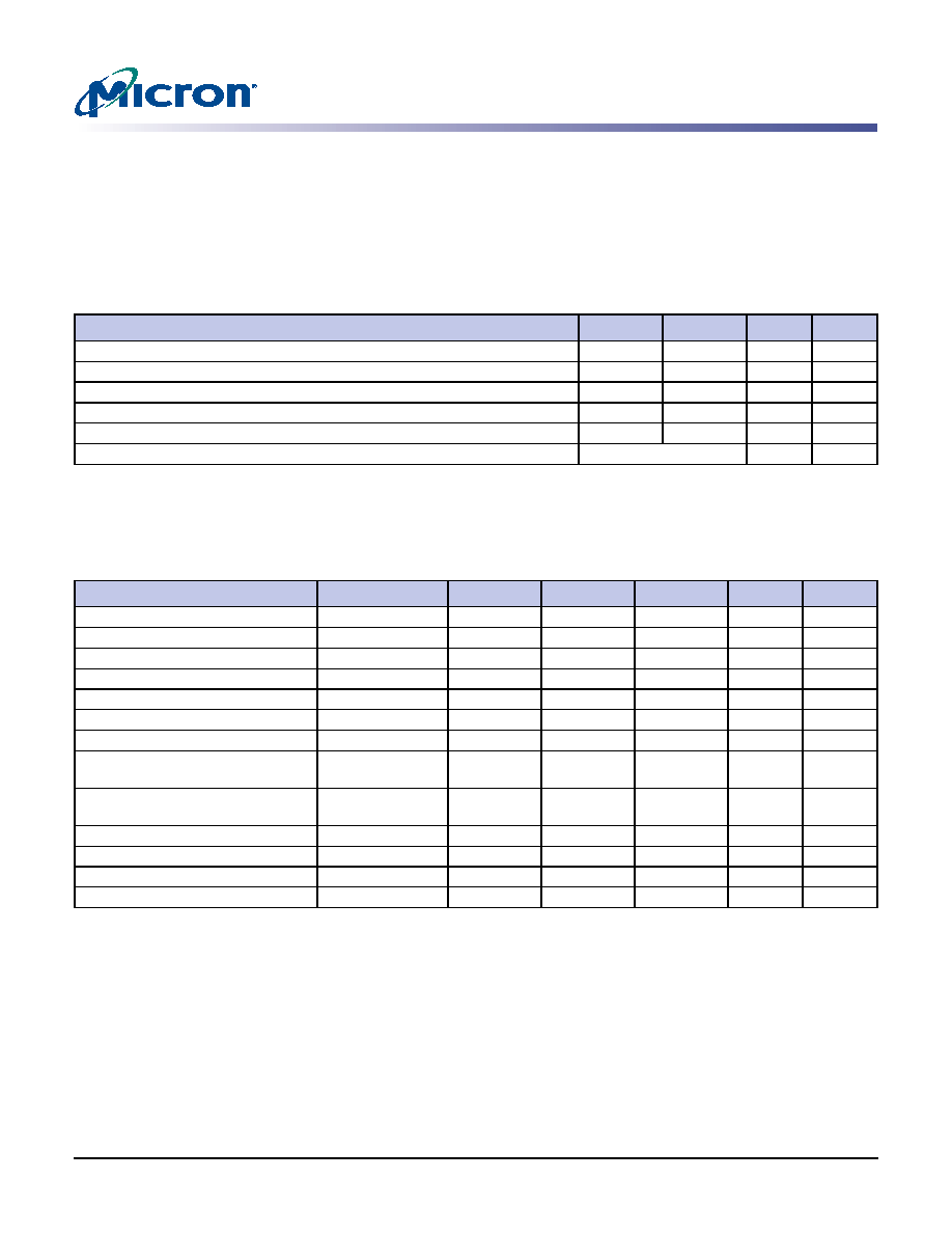
PDF: 09005aef80a41b46/Source: 09005aef809f284b
Micron Technology, Inc., reserves the right to change products or specifications without notice.
MT49H8M36_2.fm - Rev. H 8/05 EN
44
©2002 Micron Technology, Inc. All rights reserved.
288Mb: x36, x18, x9 2.5V V
EXT
, 1.8V V
DD
, HSTL, RLDRAM II
Electrical Characteristics
Electrical Characteristics
Stresses greater than those listed may cause permanent damage to the device. This is a
stress rating only, and functional operation of the device at these or any other condi-
tions above those indicated in the operational sections of this specification is not
implied. Exposure to absolute maximum rating conditions for extended periods may
affect reliability.
Notes: 1. Junction temperature depends upon package type, cycle time, loading, ambient tempera-
ture, and airflow.
Notes: 1. All voltages referenced to V
SS
(GND).
2. Typically the value of V
REF
is expect to be 0.5 x V
DD
Q of the transmitting device. V
REF
is
expected to track variations in V
DD
Q.
3. Peak-to-peak AC noise on V
REF
must not exceed ±2% V
REF
(DC).
4. Overshoot:
V
IH
(
AC
)
V
DD
+ 0.7V for t
t
CK/2.
Undershoot: V
IL
(
AC
)
-0.5V for t
t
CK/2.
During normal operation, V
DD
Q must not exceed V
DD
.
Control input signals may not have pulse widths less than
t
CK/2 or operate at frequencies
exceeding
t
CK (MAX).
5. V
DD
Q can be set to a nominal 1.5V + 0.1V or 1.8V + 0.1V supply.
6. I
OH
and I
OL
are defined as absolute values and are measured at V
DD
Q/2. I
OH
flows from the
device, I
OL
flows into the device.
Figure 38: Absolute Maximum Ratings
Parameter
Min
Max
Units
Notes
Storage temperature
-55
+150
∞C
I/O voltage
-0.3V
V
DD
Q + 0.3
V
Voltage on V
EXT
supply relative to V
SS
-0.3
+2.8
V
Voltage on V
DD
supply relative to V
SS
-0.3
+2.1
V
Voltage on V
DD
Q supply relative to V
SS
-0.3
+2.1
V
Junction temperature
110
∞C
1
Table 22:
DC Electrical Characteristics and Operating Conditions
+0∞C
T
C
+95∞C; +1.7V V
DD
+1.9V, unless otherwise noted
Description
Condition
Symbol
Min
Max
Units
Notes
Supply voltage
V
EXT
2.38
2.63
V
1
Supply voltage
V
DD
1.7
1.9
V
1, 4
Isolated output ouffer supply
V
DD
Q
1.4
V
DD
V
1, 4, 5
Reference voltage
V
REF
0.49 ◊ V
DD
Q
0.51 ◊ V
DD
Q
V
1≠3, 8
Termination voltage
V
TT
0.95 ◊ V
REF
1.05 ◊ V
REF
V
9, 10
Input high (Logic 1) voltage
V
IH
V
REF
+ 0.1
V
DD
Q + 0.3
V
1, 4
Input low (Logic 0) voltage
V
IL
V
SS
Q - 0.3
V
REF
- 0.1
V
1, 4
Output high current
V
OH
= V
DD
Q/2
I
OH
(V
DD
Q/2) /
(1.15 ◊ RQ/5)
(V
DD
Q/2) /
(0.85 ◊ RQ/5)
mA
6, 7, 11
Output low current
V
OL
= V
DD
Q/2
I
OL
(V
DD
Q/2) /
(1.15 ◊ RQ/5)
(V
DD
Q/2) /
(0.85 ◊ RQ/5)
mA
6, 7, 11
Clock input leakage current
0V
V
IN
V
DD
I
LC
-5
5
µA
Input leakage current
0V
V
IN
V
DD
I
LI
-5
5
µA
Output leakage current
0V
V
IN
V
DD
Q
I
LO
-5
5
µA
Reference voltage current
I
REF
-5
5
µA
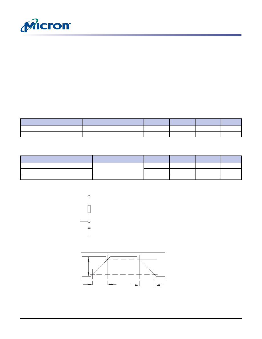
PDF: 09005aef80a41b46/Source: 09005aef809f284b
Micron Technology, Inc., reserves the right to change products or specifications without notice.
MT49H8M36_2.fm - Rev. H 8/05 EN
45
©2002 Micron Technology, Inc. All rights reserved.
288Mb: x36, x18, x9 2.5V V
EXT
, 1.8V V
DD
, HSTL, RLDRAM II
Electrical Characteristics
7. If MRS bit A8 is 0, use RQ = 250
in the equation in lieu of presence of an external imped-
ance matched resistor.
8. V
REF
is expected to equal V
DD
Q/2 of the transmitting device and to track variations in the
DC level of the same. Peak-to-peak noise (non-common mode) on V
REF
may not exceed
±2% of the DC value. Thus, from V
DD
Q/2, V
REF
is allowed ±2%V
DD
Q/2 for DC error and an
additional ±2%V
DD
Q/2 for AC noise. This measurement is to be taken at the nearest V
REF
bypass capacitor.
9. V
TT
is expected to be set equal to V
REF
and must track variations in the DC level of V
REF
.
10. On-die termination may be selected using mode register bit 9 (see Figure 8 on page 18). A
resistance R
TT
from each data input signal to the nearest V
TT
can be enabled. R
TT
= 150
(±10%) at 70∞C T
C
.
11. For V
OL
and V
OH
, refer to the RLDRMA II HSpice or IBIS driver models.
Figure 39: Output Test Conditions
Figure 40: Input Waveform
Table 23:
AC Electrical Characteristics and Operating Conditions
+0∞C
Tc +95∞C; +1.7V V
DD
+1.9V, unless otherwise noted
Description
Conditions
Symbol
Min
Max
Units
Input high (Logic 1) voltage
Matched impedance mode
V
IH
V
REF
+ 0.2
V
DD
Q + 0.3
V
Input low (Logic 0) voltage
Matched impedance mode
V
IL
V
SS
Q - 0.3
V
REF
- 0.2
V
Table 24:
Capacitance
Description
Conditions
Symbol
Min
Max
Units
Address/Control input capacitance
T
A
= 25∞C; f = 1 MHz
C
I
1.5
2.5
pF
I/O capacitance (DQ, DM, QK)
C
O
3.5
5.0
pF
Clock capacitance
C
CK
2.0
3.0
pF
10pF
DQ
50
V
TT
Test point
V
IH
(
AC
) MIN
V
IL
(
AC
) MAX
Rise Time:
2 V/ns
Fall Time:
2 V/ns
V
DD
Q
GND
V
SWING

PDF: 09005aef80a41b46/Source: 09005aef809f284b
Micron Technology, Inc., reserves the right to change products or specifications without notice.
MT49H8M36_2.fm - Rev. H 8/05 EN
46
©2002 Micron Technology, Inc. All rights reserved.
288Mb: x36, x18, x9 2.5V V
EXT
, 1.8V V
DD
, HSTL, RLDRAM II
Electrical Characteristics
Table 25:
I
DD
Operating Conditions and Maximum Limits
Notes 1≠6 on page 47
Description
Condition
Symbol
Max
Units
-25
-33
-5
Standby current
t
CK = Idle
All banks idle, no inputs toggling
I
SB
1 (V
DD
)
X
36
48
48
48
mA
I
SB
1 (V
DD
)
X
18/
X
9
48
48
48
I
SB
1 (V
EXT
)
26
26
26
Active standby
current
CS# = 1
No commands, half bank/address/data change
once every four clock cycles
ISB2 (V
DD
)
X
36
288
233
189
mA
I
SB
2 (V
DD
)
X
18/
X
9
288
233
189
I
SB
2 (V
EXT
)
26
26
26
Operational
current
BL = 2, sequential bank access, bank transitions
once every
t
RC, half address transitions once
every
t
RC, read followed by write sequence,
continous data during WRITE commands.
I
DD
1 (V
DD
)
X
36
374
343
292
mA
I
DD
1 (V
DD
)
X
18/
X
9
348
305
255
I
DD
1 (V
EXT
)
41
36
36
Operational
current
BL = 4, sequential bank access, bank transitions
once every
t
RC, half address transitions once
every
t
RC, read followed by write sequence,
continous data during WRITE commands.
I
DD
2 (V
DD
)
X
36
418
389
339
mA
I
DD
2 (V
DD
)
X
18/
X
9
362
319
269
I
DD
2 (V
EXT
)
48
42
42
Operational
current
BL = 8, sequential bank access, bank transitions
once every
t
RC, half address transitions once
every
t
RC, read followed by write sequence,
continous data during WRITE commands.
I
DD
3 (V
DD
)
X
36
NA
NA
NA
mA
I
DD
3 (V
DD
)
X
18/
X
9
408
368
286
I
DD
3 (V
EXT
)
55
48
48
Burst refresh
current
Eight bank cyclic refresh, continous address/
data, command bus remains in refresh for all
eight banks.
I
REF
1 (V
DD
)
X
36
685
545
375
mA
I
REF
1 (V
DD
)
X
18/
X
9
680
530
367
I
REF
1 (V
EXT
)
133
111
105
Distributed
refresh current
Single bank refresh, sequential bank access,
half address transitions once every
t
RC,
continous data.
I
REF
2 (V
DD
)
X
36
326
281
227
mA
I
REF
2 (V
DD
)
X
18/
X
9
325
267
221
I
REF
2 (V
EXT
)
48
42
42
Operating burst
write current
example
BL = 2, cyclic bank access, half of address bits
change every clock cycle, continuous data,
measurement is taken during continuous
WRITE.
I
DD
2
W
(V
DD
)
X
36
990
914
676
mA
I
DD
2
W
(V
DD
)
X
18/
X
9
970
819
597
I
DD
2
W
(V
EXT
)
100
90
69
Operating burst
write current
example
BL = 4, cyclic bank access, half of address bits
change every two clocks, continuous data,
measurement is taken during continuous
WRITE.
I
DD
4
W
(V
DD
)
X
36
882
790
567
mA
I
DD
4
W
(V
DD
)
X
18/
X
9
779
609
439
I
DD
4
W
(V
EXT
)
88
77
63
Operating burst
write current
example
BL = 8, cyclic bank access, half of address bits
change every four clock cycles, continuous
data, measurement is taken during continuous
WRITE.
I
DD
8
W
(V
DD
)
X
36
NA
NA
NA
mA
I
DD
8
W
(V
DD
)
X
18/
X
9
668
525
364
I
DD
8
W
(V
EXT
)
60
51
40
Operating burst
read current
example
BL = 2, cyclic bank access, half of address bits
change every clock cycle, measurement is taken
during continuous READ.
I
DD
2R (V
DD
)
X
36
920
850
628
mA
I
DD
2
R
(V
DD
)
X
18/
X
9
902
761
555
I
DD
2
R
(V
EXT
)
100
90
69
Operating burst
read current
example
BL = 4, cyclic bank access, half of address bits
change every two clocks, measurement is taken
during continuous READ.
I
DD
4
R
(V
DD
)
X
36
764
734
527
mA
I
DD
4
R
(V
DD
)
X
18/
X
9
724
566
408
I
DD
4
R
(V
EXT
)
88
77
63
Operating burst
read current
example
BL = 8, cyclic bank access, half of address bits
change every four clock cycles, measurement is
taken during continuous READ.
I
DD
8
R
(V
DD
)
X
36
NA
NA
NA
mA
I
DD
8
R
(V
DD
)
X
18/
X
9
621
488
338
I
DD
8
R
(V
EXT
)
60
51
40

PDF: 09005aef80a41b46/Source: 09005aef809f284b
Micron Technology, Inc., reserves the right to change products or specifications without notice.
MT49H8M36_2.fm - Rev. H 8/05 EN
47
©2002 Micron Technology, Inc. All rights reserved.
288Mb: x36, x18, x9 2.5V V
EXT
, 1.8V V
DD
, HSTL, RLDRAM II
Electrical Characteristics
Notes: 1. I
DD
specifications are tested after the device is prop erly initialized. +0∞C
Tc +95∞C;
+1.7V
V
DD
+1.9V, +2.38V V
EXT
+2.63V, +1.4V V
DD
Q
+1.6V, V
REF
= V
DD
Q/2.
2.
t
CK =
t
DK = MIN,
t
RC = MIN.
3. Input slew rate is specified in Table 22, DC Electrical Characteristics and Operating Condi-
tions, on page 44.
4. Definitions for I
DD
conditions:
a. LOW is defined as V
IN
V
IL
(
AC
) MAX.
b. HIGH is defined as V
IN
V
IH
(
AC
) MAX.
c. Stable is defined as inputs remaining at a HIGH or LOW level.
d. Floating is defined as inputs at V
REF
= V
DD
Q/2.
e. Continous data is defined as half the DQ signals changing between HIGH and LOW
every half clock cycle (twice per clock).
f. Continous address is defined as half the address signals changing between HIGH and
LOW every clock cycle (once per clock).
g. Sequential bank access is defined as the bank address incrementing by one ever
t
RC.
h. Cyclic bank access is defined as the bank address incrementing by one for each com-
mand access. For BL = 4 this is every other clock.
5. CS# is HIGH unless a READ, WRITE, AREF, or MRS command is registered. CS# never transis-
tions more tha n once per clock cycle.
6. I
DD
parameters are specified with ODT disabled.
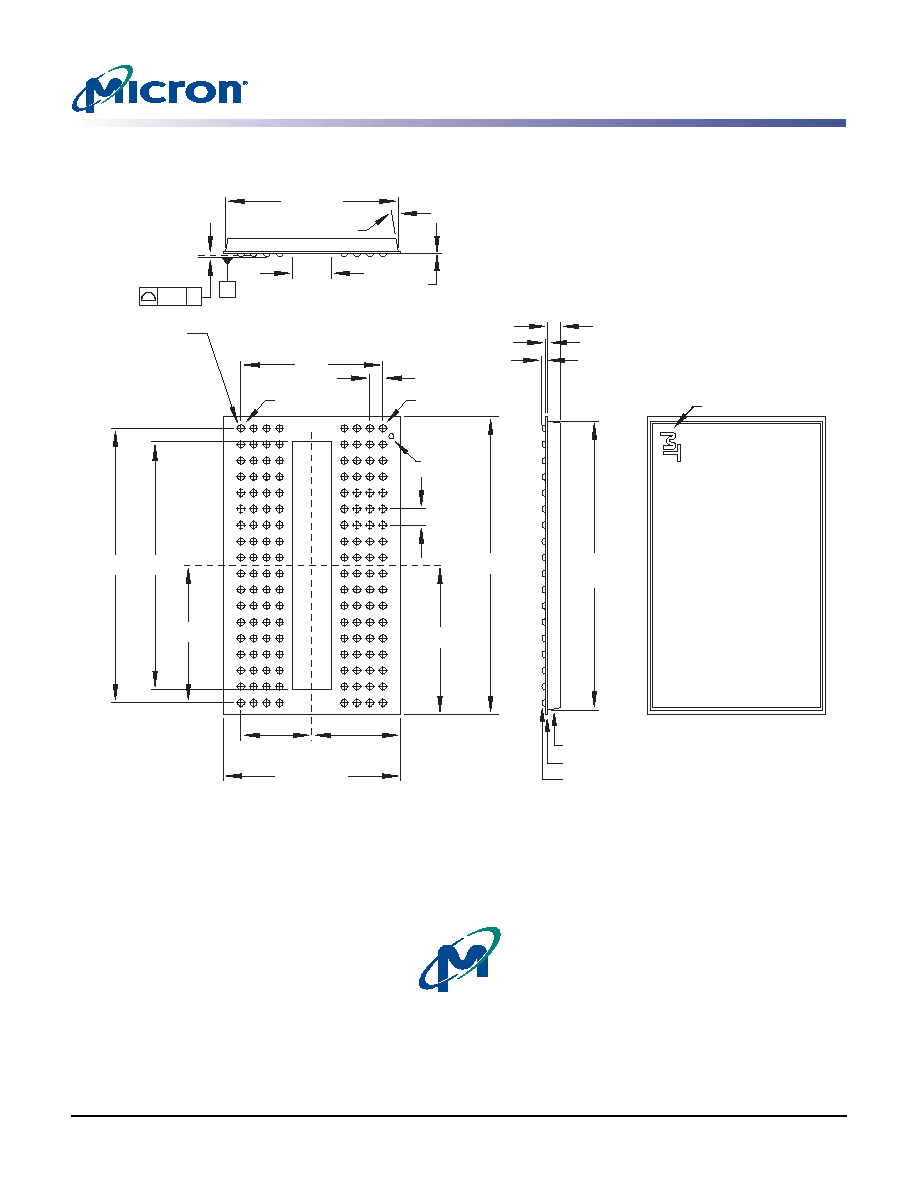
Æ
8000 S. Federal Way, P.O. Box 6, Boise, ID 83707-0006, Tel: 208-368-3900
prodmktg@micron.com www.micron.com Customer Comment Line: 800-932-4992
Micron, the M logo, and the Micron logo are trademarks of Micron Technology, Inc.
RLDRAM is a trademark of Infineon Technologies AG in various countries, and is used by Micron Technology, Inc. under
license from Infineon. All other trademarks are the property of their respective owners.
This data sheet contains minimum and maximum limits specified over the complete power supply and temperature range
for production devices. Although considered final, these specifications are subject to change, as further product
development and data characterization sometimes occur.
288Mb: x36, x18, x9 2.5V V
EXT
, 1.8V V
DD
, HSTL, RLDRAM II
Package Dimensions
PDF: 09005aef80a41b46/Source: 09005aef809f284b
Micron Technology, Inc., reserves the right to change products or specifications without notice.
MT49H8M36_2.fm - Rev. H 8/05 EN
48
©2002 Micron Technology, Inc. All rights reserved.
Package Dimensions
Figure 41: 144-Ball µBGA
Notes: 1. All dimensions in millimeters.
BALL A1 ID
17.90
CTR
0.44 ±0.05
0.39 ±0.05
0.26 ±0.05
BALL A1
BALL A12
0.08 A
A
SEATING PLANE
10∫ TYP
0.08 MAX
10.70 CTR
11.00 ±0.10
4.40
5.50 ±0.05
8.80
2.40 CTR
0.80 TYP
1.00 TYP
9.25 ±0.05
8.50
15.40
17.00
18.50 ±0.10
144X
0.45
DIMENSIONS APPLY
TO SOLDER BALLS
POST REFLOW. THE
PRE-REFLOW BALL
DIAMETER IS 0.50 ON
A 0.40 SMD BALL PAD.
BALL A1 ID
MOLD COMPOUND: EPOXY NOVOLAC
SUBSTRATE: PLASTIC LAMINATE
SOLDER BALL MATERIAL:
62% Sn, 36% Pb, 2%Ag OR
96.5% Sn, 3%Ag, 0.5% Cu

PDF: 09005aef80a41b46/Source: 09005aef809f284b
Micron Technology, Inc., reserves the right to change products or specifications without notice.
MT49H8M36_2.fm - Rev. H 8/05 EN
49
©2002 Micron Technology, Inc. All rights reserved.
288Mb: x36, x18, x9 2.5V V
EXT
, 1.8V V
DD
, HSTL, RLDRAM II
Package Dimensions
Rev. J . . . . . . . . . . . . . . . . . . . . . . . . . . . . . . . . . . . . . . . . . . . . . . . . . . . . . . . . . . . . . . . . . . . . . . . . . . . . . . . . . . . . . . . . . . . . . . . . 8/05
∑ Updated Table 25, I
DD
Operating Conditions and Maximum Limits, on page 46.
∑ Added operating temperature ranges.
∑ Updated package drawing to include unleaded information.
∑ Updated template.
Rev H . . . . . . . . . . . . . . . . . . . . . . . . . . . . . . . . . . . . . . . . . . . . . . . . . . . . . . . . . . . . . . . . . . . . . . . . . . . . . . . . . . . . . . . . . . . . . . 11/04
∑ Production status.
Rev G . . . . . . . . . . . . . . . . . . . . . . . . . . . . . . . . . . . . . . . . . . . . . . . . . . . . . . . . . . . . . . . . . . . . . . . . . . . . . . . . . . . . . . . . . . . . . . 09/04
∑ Added updated note to BS table
∑ QK, QK# description updated (Page 10).
∑ JTAG logic levels update (Pages 10, 35).
∑ Timing parameters (Power-up sequence in Figure 7 updated (Page 14).
∑ Clock Considerations "DLL auto reset" removed (Page 15).
∑ Figure 8 Vid(DC) and Vid(AC) updated (Page 16).
∑ Figure 16 QVLD signal corrected (Page 21).On-die termination text updated to include DM pin (Page 27).
∑ Measured temperature for R
TT
changed to
70∞C Tc
(Pages 27, 41).
∑ Figure 27 QVLD signal corrected (Page 27).
∑ Figure 33 text and notes updated to correct Address bits (Page 31).
∑ Power-up sequence in Figure 34 updated (Page 31).
∑ Measured temperatures and range changed to
+0∞C
Tc +95∞C
(Pages 37, 38, 41,42, 43).
∑ TAP DC parameters (V
OL
1, V
OL
2, V
OH
1, V
OH
2) updated (Page 38).
∑ I/O Capacitance updated (Page 42).
∑