
ADVANCE
1
256: x16, x32 RLDRAM
©2002, Micron Technology, Inc.
MT49H8M32_3.p65 ≠ Rev. 3, Pub. 6/02
256Mb: x16, x32
2.5V V
EXT
, 1.8V V
DD
, 1.8V V
DD
Q, RLDRAM
PRODUCTS AND SPECIFICATIONS DISCUSSED HEREIN ARE FOR EVALUATION AND REFERENCE PURPOSES ONLY AND ARE SUBJECT TO CHANGE BY
MICRON WITHOUT NOTICE. PRODUCTS ARE ONLY WARRANTED BY MICRON TO MEET MICRON'S PRODUCTION DATA SHEET SPECIFICATIONS.
REDUCED LATENCY
DRAM (RLDRAM)
FEATURES
∑ 2.5V V
EXT
, 1.8V V
DD
, 1.8V V
DD
Q I/O
∑ Cyclic bank addressing for maximum data out
bandwidth
∑ Non-multiplexed addresses
∑ Non-interruptible sequential burst of two (2-bit
prefetch) and four (4-bit prefetch) DDR
∑ Target 600 Mb/s/p data rate
∑ Programmable Read Latency (RL) of 5-8
∑ Data valid signal (DVLD) activated as read data is
available
∑ Data Mask signals (DM0/DM1) to mask first and
second part of write data burst
∑ IEEE 1149.1 compliant JTAG boundary scan
∑ Pseudo-HSTL 1.8V I/O Supply
∑ Internal Auto Precharge
∑ Refresh requirements: 32ms at 100∞C junction
temperature (8K refresh for each bank, 64K refresh
command must be issued in total each 32ms)
OPTIONS
MARKING
∑ Clock Cycle Timing
3.3ns (300 MHz)
-3.3
4ns (250 MHz)
-4
5ns (200 MHz)
-5
∑ Configuration
8 Meg x 32
MT49H8M32FM
(1 Meg x 32 x 8 banks)
16 Meg x 16
MT49H16M16FM
(2 Meg x 16 x 8 banks)
∑ Package
144-ball, 11mm x 18.5mm T-FBGA
FM
144-Ball T-FBGA
MT49H8M32 ≠ 1 Meg x 32 x 8 banks
MT49H16M16 ≠ 2 Meg x 16 x 8 banks
For the latest data sheet, please refer to the Micron
Web site:
www.micron.com/dramds
GENERAL DESCRIPTION
The Micron
Æ
256Mb Reduced Latency DRAM
(RLDRAM) contains 8 banks x32Mb of memory acces-
sible with 32-bit or 16-bit I/Os in a double data rate (DDR)
format where the data is provided and synchronized with
a differential echo clock signal. RLDRAM does not require
VALID PART NUMBERS
PART NUMBER
DESCRIPTION
MT49H8M32FM-xx
8 Meg x 32
MT49H16M16FM-xx
16 Meg x 16
row/column address multiplexing and is optimized for
fast random access and high-speed bandwidth.
RLDRAM is designed for communication data
storages like transmit or receive buffers in telecommuni-
cation systems as well as data or instruction cache
applications requiring large amounts of memory.
POWER-UP INITIALIZATION
Since the RLDRAM does not have a designated reset
function, the following procedure must be executed in
order to initalize the internal state machine, regulators,
and force the DRAM to be in ready state.
∑ Apply power, then start clock
∑ After power on, an initial pause of 200µs is required
∑ MRS command for 2 clocks and set standard mode
register for 1 clock (2 dummies plus 1 valid MRS set)
∑ 8 refresh cycles (minimum), one on each bank and
separated by 2,048 cycles (
t
MRSC must be satisfied
between MRS and first REF command)
∑ Ready for normal operation (
t
RC cycles after the last
refresh command)
2
256: x16, x32 RLDRAM
Micron Technology, Inc., reserves the right to change products or specifications without notice.
MT49H8M32_3.p65 ≠ Rev. 3, Pub. 6/02
©2002, Micron Technology, Inc.
ADVANCE
256Mb: x16, x32
2.5V V
EXT
, 1.8V V
DD
, 1.8V V
DD
Q, RLDRAM
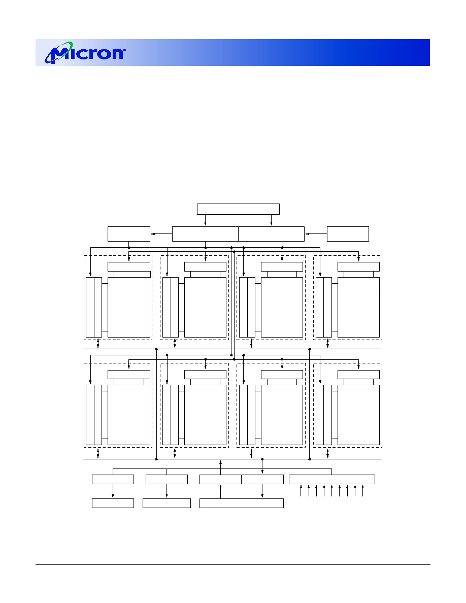
NOTE: 1. When the BL4 setting is used, A18 is a "Don't Care."
FUNCTIONAL BLOCK DIAGRAM
8 Meg x 32
A0≠A18, B0, B1, B2
Column Address
Buffer
Column Address
Counter
Refresh
Counter
Row Decoder
Memory Array
Bank 1
Column Decoder
Sense Amp and Data Bus
Row Address
Buffer
Row Decoder
Memory Array
Bank 0
Column Decoder
Sense Amp and Data Bus
Row Decoder
Memory Array
Bank 2
Column Decoder
Sense Amp and Data Bus
Row Decoder
Memory Array
Bank 3
Column Decoder
Sense Amp and Data Bus
Row Decoder
Memory Array
Bank 5
Column Decoder
Sense Amp and Data Bus
Row Decoder
Memory Array
Bank 4
Column Decoder
Sense Amp and Data Bus
Row Decoder
Memory Array
Bank 6
Column Decoder
Sense Amp and Data Bus
Row Decoder
Memory Array
Bank 7
Column Decoder
CK
CK
#
AS#
WE#
CS#
REF#
DM0
DM1
V
REF
Sense Amp and Data Bus
Data Valid
DVLD
Data Read Strobe
DQS[3:0], DQS#[3:0]
Input Buffers
Output Buffers
Control Logic and Timing Generator
DQ0≠DQ31
POWER-DOWN
Because the RLDRAM uses multiple power supply
voltage, the following sequence is required for power-
down.
∑ Take all input signals to be V
SS
or High-Z
It is recommended to place Schottky diodes on the
board between the 2.5V and 1.8V power supplies.
3
256: x16, x32 RLDRAM
Micron Technology, Inc., reserves the right to change products or specifications without notice.
MT49H8M32_3.p65 ≠ Rev. 3, Pub. 6/02
©2002, Micron Technology, Inc.
ADVANCE
256Mb: x16, x32
2.5V V
EXT
, 1.8V V
DD
, 1.8V V
DD
Q, RLDRAM
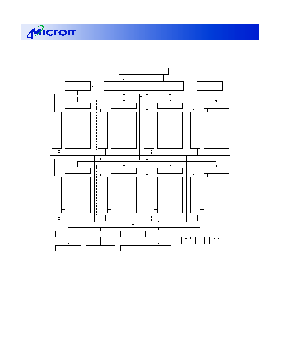
NOTE: 1. When the BL4 setting is used, A19 is a "Don't Care."
2. In the 16 Meg x 16 configuration, only DQS[1:0] and DQS#[1:0] are used.
FUNCTIONAL BLOCK DIAGRAM
16 Meg x 16
A0≠A19, B0, B1, B2
Column Address
Buffer
Column Address
Counter
Refresh
Counter
Row Decoder
Memory Array
Bank 1
Column Decoder
Sense Amp and Data Bus
Row Address
Buffer
Row Decoder
Memory Array
Bank 0
Column Decoder
Sense Amp and Data Bus
Row Decoder
Memory Array
Bank 2
Column Decoder
Sense Amp and Data Bus
Row Decoder
Memory Array
Bank 3
Column Decoder
Sense Amp and Data Bus
Row Decoder
Memory Array
Bank 5
Column Decoder
Sense Amp and Data Bus
Row Decoder
Memory Array
Bank 4
Column Decoder
Sense Amp and Data Bus
Row Decoder
Memory Array
Bank 6
Column Decoder
Sense Amp and Data Bus
Row Decoder
Memory Array
Bank 7
Column Decoder
CK
CK#
AS#
WE#
CS#
REF#
DM0
DM1
V
REF
Sense Amp and Data Bus
Data Valid
DVLD
Data Read Strobe
DQS[1:0], DQS#[1:0]
Input Buffers
Output Buffers
Control Logic and Timing Generator
DQ0≠DQ15

4
256: x16, x32 RLDRAM
Micron Technology, Inc., reserves the right to change products or specifications without notice.
MT49H8M32_3.p65 ≠ Rev. 3, Pub. 6/02
©2002, Micron Technology, Inc.
ADVANCE
256Mb: x16, x32
2.5V V
EXT
, 1.8V V
DD
, 1.8V V
DD
Q, RLDRAM
TABLE OF CONTENTS
General Description .......................................................
1
Power-Up Initialization ...................................................
1
Functional Block Diagram, 8 Meg x 32 ................
2
Power-Down ...................................................................
2
Functional Block Diagram, 16 Meg x 16 .............
3
8 Meg x 32 Ball Assignment (Top View)
144-Ball T-FBGA ...............................................
5
16 Meg x 16 PIN Assignment (Top View)
144-Ball T-FBGA ...............................................
5
Ball Descriptions ....................................................
6
Ball Descriptions (continued) ................................
7
Truth Table 1 ..........................................................
8
Programming Description ..............................................
9
RLDRAM Programming Table ..............................
9
Mode Register Description ............................................ 10
Mode Register Command Table ........................... 10
IEEE 1149.1 Serial Boundary Scan (JTAG) ................ 11
Disabling the JTAG Feature .......................................... 11
Figure 1, TAP Controller State Diagram .............. 11
Test Access Port (TAP) .................................................. 11
Test Clock (TCK) ........................................................ 11
Test MODE SELECT (TMS) ...................................... 11
Test Data-In (TDI) ...................................................... 11
Test Data-Out (TDO) ................................................. 12
Performing a TAP Reset ........................................... 12
TAP Registers ............................................................ 12
Instruction Register .................................................... 12
Figure 2, TAP Controller Block Diagram ............. 12
Bypass Register ......................................................... 12
Boundary Scan Register ........................................... 12
Identification (ID) Register ........................................ 13
TAP Instruction Set ........................................................ 13
Overview ..................................................................... 13
Extest .......................................................................... 13
Idcode ......................................................................... 13
Sample Z .................................................................... 13
Sample/Preload ......................................................... 13
Bypass ........................................................................ 14
TAP Timing ............................................................. 14
TAP AC Electrical Characteristics ........................ 14
Reserved .................................................................... 14
TAP DC Electrical Characteristics and
Operating Conditions ........................................ 15
Identification Register Definitions ........................ 16
Scan Register Sizes .............................................. 16
Instruction codes ................................................... 16
Boundary Scan (Exit) Order ................................. 17
Absolute Maximum Ratings .......................................... 18
Recommended DC Operation Ranges ........................ 18
DC Electrical Characteristics and
Operating Conditions ........................................ 18
DC Electrical Characteristics and
Operating Conditions ........................................ 19
I
DD
Electrical Characteristics and
Operating Conditions ........................................ 20
Capacitance ........................................................... 21
AC Electrical Characteristics and
Operating Conditions ........................................ 21
AC Electrical Characteristics ................................ 22
Timing Waveforms
General Overview and Timing Definition
(BL2/WL2) .......................................................... 23
READ Timing (BL = 2) ........................................... 24
READ Timing (BL = 4) ........................................... 25
WRITE Timing (BL = 2, RL = 6) ........................... 26
WRITE Timing (BL = 4, RL = 6) ........................... 27
READ to WRITE Timing (BL = 2, WL = 2) .......... 28
WRITE to READ Timing (BL = 2, WL = 2) .......... 29
Refresh Timing ....................................................... 30
Example of Refresh Implementation
(Cyclic Bank Burst Refresh) ............................. 31
WRITE Data Mask Timing (BL = 2, WL = 2) ....... 32
WRITE Data Mask Timing (BL = 4, WL = 1) ....... 33
WRITE/READ and READ/WRITE Timing, Cyclic
Bank Access (RL = 6, BL = 2, WL = 3) ........... 34
WRITE/READ and READ/WRITE Timing, Cyclic
Bank Access (RL = 5, BL = 2, WL = 2) ........... 35
WRITE/READ and READ/WRITE Timing, Cyclic
Bank Access (RL = 6, BL = 4, WL = 2) ........... 36
WRITE/READ and READ/WRITE Timing, Cyclic
Bank Access (RL = 5, BL = 4, WL = 1) ........... 37
Random Access, Single Bank
(RL = 6, BL = 2, WL = 3) ................................... 38
Random Access, Single Bank
(RL = 5, BL = 2, WL = 2,
t
RC = 6) .................... 39
Random Access, Single Bank
(RL = 6, BL = 4, WL = 2) ................................... 40
Random Access, Single Bank
(RL = 5, BL = 4, WL = 1,
t
RC = 6) .................... 41
Package Drawing
144-Ball T-FBGA .................................................... 42

5
256: x16, x32 RLDRAM
Micron Technology, Inc., reserves the right to change products or specifications without notice.
MT49H8M32_3.p65 ≠ Rev. 3, Pub. 6/02
©2002, Micron Technology, Inc.
ADVANCE
256Mb: x16, x32
2.5V V
EXT
, 1.8V V
DD
, 1.8V V
DD
Q, RLDRAM
8 MEG x 32 BALL ASSIGNMENT (Top View)
144-Ball T-FBGA
1
2
3
4
5
6
7
8
9
10
11
12
A
V
SS
V
EXT
V
REF
V
SS
V
SS
V
EXT
TMS
TCK
B
V
SS
DQ8
DQ9
V
SS
Q
V
SS
Q
DQ1
DQ0
V
SS
C
V
SS
DQ10
DQ11
V
DD
Q
V
DD
Q
DQ3
DQ2
V
SS
D
V
SS
DQS1 DQS1#
V
SS
Q
V
SS
Q
DQS0# DQS0
V
SS
E
V
SS
DQ12
DQ13
V
DD
Q
V
DD
Q
DQ5
DQ4
V
SS
F
DM0
DQ14
DQ15
V
SS
Q
V
SS
Q
DQ7
DQ6
DVLD
G
A5
A6
A7
V
DD
V
DD
A2
A1
A0
H
A8
A9
V
SS
V
SS
V
SS
V
SS
A4
A3
J
AS#
B2
V
DD
V
DD
V
DD
V
DD
B0
CK
K
WE#
REF#
V
DD
V
DD
V
DD
V
DD
B1
CK#
L
A18
CS#
V
SS
V
SS
V
SS
V
SS
A14
A13
M
A15
A16
A17
V
DD
V
DD
A12
A11
A10
N
DM1
DQ22
DQ23
V
SS
Q
V
SS
Q
DQ31
DQ30
NC
P
V
SS
DQ20
DQ21
V
DD
Q
V
DD
Q
DQ29
DQ28
V
SS
R
V
SS
DQS2 DQS2#
V
SS
Q
V
SS
Q
DQS3# DQS3
V
SS
T
V
SS
DQ18
DQ19
V
DD
Q
V
DD
Q
DQ27
DQ26
V
SS
U
V
SS
DQ16
DQ17
V
SS
Q
V
SS
Q
DQ25
DQ24
V
SS
V
V
SS
V
EXT
V
REF
V
SS
V
SS
V
EXT
TDO
TDI
16 MEG x 16 BALL ASSIGNMENT (Top View)
144-Ball T-FBGA
1
2
3
4
5
6
7
8
9
10
11
12
A
V
SS
V
EXT
V
REF
V
SS
V
SS
V
EXT
TMS
TCK
B
V
SS
NC
NC
V
SS
Q
V
SS
Q
DQ1
DQ0
V
SS
C
V
SS
NC
NC
V
DD
Q
V
DD
Q
DQ3
DQ2
V
SS
D
V
SS
NC
NC
V
SS
Q
V
SS
Q
DQS0# DQS0
V
SS
E
V
SS
NC
NC
V
DD
Q
V
DD
Q
DQ5
DQ4
V
SS
F
DM0
NC
NC
V
SS
Q
V
SS
Q
DQ7
DQ6
DVLD
G
A5
A6
A7
V
DD
V
DD
A2
A1
A0
H
A8
A9
V
SS
V
SS
V
SS
V
SS
A4
A3
J
AS#
B2
V
DD
V
DD
V
DD
V
DD
B0
CK
K
WE#
REF#
V
DD
V
DD
V
DD
V
DD
B1
CK#
L
A19
CS#
V
SS
V
SS
V
SS
V
SS
A14
A13
M
A15
A16
A17
V
DD
V
DD
A12
A11
A10
N
DM1
NC
NC
V
SS
Q
V
SS
Q
DQ15
DQ14
A18
P
V
SS
NC
NC
V
DD
Q
V
DD
Q
DQ13
DQ12
V
SS
R
V
SS
NC
NC
V
SS
Q
V
SS
Q
DQS1# DQS1
V
SS
T
V
SS
NC
NC
V
DD
Q
V
DD
Q
DQ11
DQ10
V
SS
U
V
SS
NC
NC
V
SS
Q
V
SS
Q
DQ9
DQ8
V
SS
V
V
SS
V
EXT
V
REF
V
SS
V
SS
V
EXT
TDO
TDI

6
256: x16, x32 RLDRAM
Micron Technology, Inc., reserves the right to change products or specifications without notice.
MT49H8M32_3.p65 ≠ Rev. 3, Pub. 6/02
©2002, Micron Technology, Inc.
ADVANCE
256Mb: x16, x32
2.5V V
EXT
, 1.8V V
DD
, 1.8V V
DD
Q, RLDRAM
BALL DESCRIPTIONS
T-FBGA (x32) T-FBGA (x16)
SYMBOL
TYPE
DESCRIPTION
12J, 12K
12J, 12K
CK, CK#
Input
Differential input clock pair
2L
2L
CS#
Input
Chip select
1J
1J
AS#
Input
Address strobe
1K
1K
WE#
Input
Write enable
2K
2K
REF#
Input
Auto refresh
11J, 11K, 2J
11J, 11K, 2J
B[0:2]
Input
Bank select
12G, 11G, 10G, 12G, 11G, 10G,
A[0:18]
Input
Address input
12H, 11H, 1G,
12H, 11H, 1G,
A[0:19]
2G, 3G, 1H,
2G, 3G, 1H,
2H, 12M, 11M, 2H, 12M, 11M,
10M, 12L, 11L, 10M, 12L, 11L,
1M, 2M, 3M, 1L 1M, 2M, 3M,
12N, 1L
1F, 1N
1F, 1N
DM0, DM1
Input
Data Mask
11A
11A
TMS
Input
IEEE 1149.1 Test Inputs: JEDEC-standard 1.8V I/O levels.
12V
12V
TDI
These pins may be left Not Connected if the JTAG
function is not used in the circuit.
12A
12A
TCK
Input
IEEE 1149.1 Clock Input: JEDEC-standard 1.8V I/O levels.
This pin must be tied to V
SS
if the JTAG function is not
used in the circuit.
3A, 3V
3A, 3V
V
REF
Input
Input Reference Voltage: Nominally V
DD
Q/2. Provides a
reference voltage for the input buffers.
11B, 10B, 11C, 11B, 10B, 11C,
DQ0≠DQ31
Input/
Synchronous Data I/Os: Input data must meet setup and
10C, 11E, 10E,
10C, 11E, 10E,
Output
hold times around the rising edges of CK and CK#.
11F, 10F, 2B,
11F, 10F, 11U,
Output data is synchronized to DQS and DQS#.
3B, 2C, 3C, 2E, 10U, 11T, 10T,
3E, 2F, 3F, 2U, 11P, 10P, 11N,
3U, 2T, 3T, 2P,
10N
3P, 2N, 3N,
11U, 10U, 11T,
10T, 11P, 10P,
11N, 10N
11D, 2D, 2R,
11D, 11R,
DQS0≠3 (x32) Output
Differential data read strobe
11R, 10D, 3D,
10D, 10R
DQS#0≠3 (x32)
3R, 10R
DQS0≠1 (x16)
DQS#0≠1 (x16)
12F
12F
DVLD
Output
Data Valid
11V
11V
TDO
Output
IEEE 1149.1 Test Output: JEDEC-standard 1.8V I/O level.
2A, 2V,
2A, 2V,
V
EXT
Supply
Power Supply: 2.5V nominal. See DC Electrical
10A, 10V
10A, 10V
Characteristics and Operating Condidtions for range.
3J, 3K, 4G,
3J, 3K, 4G,
V
DD
Supply
Power Supply: 1.8V nominal. See DC Electrical
4J, 4K, 4M,
4J, 4K, 4M,
Characteristics and Operating Conditions for range.
9G, 9J, 9K,
9G, 9J, 9K,
9M, 10J, 10K
9M, 10J, 10K
(continued on next page)

7
256: x16, x32 RLDRAM
Micron Technology, Inc., reserves the right to change products or specifications without notice.
MT49H8M32_3.p65 ≠ Rev. 3, Pub. 6/02
©2002, Micron Technology, Inc.
ADVANCE
256Mb: x16, x32
2.5V V
EXT
, 1.8V V
DD
, 1.8V V
DD
Q, RLDRAM
BALL DESCRIPTIONS (continued)
T-FBGA (x32) T-FBGA (x16)
SYMBOL
TYPE
DESCRIPTION
4C, 4E, 4P,
4C, 4E, 4P,
V
DD
Q
Supply
Power Supply: Isolated Output Buffer Supply. Nominally
4T, 9C, 9E,
4T, 9C, 9E,
1.8V. See DC Electrical Characteristics and Operating
9P, 9T
9P, 9T
Conditions for range.
1A≠E, 1P≠V,
1A≠E, 1P≠V,
V
SS
Supply
Power Supply: GND.
3H, 3L, 4A,
3H, 3L, 4A,
4H, 4L, 4V,
4H, 4L, 4V,
9A, 9H, 9L,
9A, 9H, 9L,
9V, 10H, 10L,
9V, 10H, 10L,
12B≠E, 12P≠U
12B≠E, 12P≠U
4B, 4D, 4F,
4B, 4D, 4F,
V
SS
Q
Supply
Power Supply: Isolated Output Buffer Supply. GND.
4N, 4R, 4U,
4N, 4R, 4U,
9B, 9D, 9F,
9B, 9D, 9F,
9N, 9R, 9U
9N, 9R, 9U
12N
2B≠2F, 2N≠2U,
NC
≠
No Connect: These signals are not internally connected
3B≠3F, 3N≠3U
and may be connected to ground to improve package
heat dissipation.

8
256: x16, x32 RLDRAM
Micron Technology, Inc., reserves the right to change products or specifications without notice.
MT49H8M32_3.p65 ≠ Rev. 3, Pub. 6/02
©2002, Micron Technology, Inc.
ADVANCE
256Mb: x16, x32
2.5V V
EXT
, 1.8V V
DD
, 1.8V V
DD
Q, RLDRAM
TRUTH TABLE
1
OPERATION
CS#
AS#
WE#
REF#
A[19:0]
2
B[2:0]
DM[1:0]
READ Cycle
L
L
H
H
VALID
VALID
X
WRITE Cycle
L
L
L
H
VALID
VALID
VALID
NOP: No operation
L
H
H
H
X
X
X
Deselect
H
X
X
X
X
X
X
Auto Refresh
L
H
H
L
X
VALID
X
MRS: Mode Register Set
3
L
L
L
L
VALID
X
X
NOTE: 1. X = "Don't Care."
H = logic HIGH.
L = logic LOW.
2. In the x32 configuration A19 is not used.
3. Only A17≠A0 are used for the Mode Register Set Command.

9
256: x16, x32 RLDRAM
Micron Technology, Inc., reserves the right to change products or specifications without notice.
MT49H8M32_3.p65 ≠ Rev. 3, Pub. 6/02
©2002, Micron Technology, Inc.
ADVANCE
256Mb: x16, x32
2.5V V
EXT
, 1.8V V
DD
, 1.8V V
DD
Q, RLDRAM
PROGRAMMING DESCRIPTION
The following table shows, for three operating frequen-
cies, the different RLDRAM configurations that can be
programmed into the Mode Register. The Read Latency
(RL) values and the Write Latencies (WL) used by the
RLDRAM Programming Table
NOTE: 1. The speed sort -3.3 provides part functional up to 300 MHz in the configurations 4, 5,
and 6 only.
The functionality of the configurations 1, 2, and 3 is not guaranteed for speed sort -
3.3.
2. The speed sort -4 provides part functional up to 250 MHz in the configurations 3, 4, 5,
and 6 only.
The functionality of the configurations 1 and 2 is not guaranteed for speed sort -4.
3. The speed sort -5 provides part functional up to 200 MHz in all configurations.
RLDRAM for the two Burst Lengths (BL) are also indi-
cated. Finally, the minimum allowed
t
RC in clock cycles
and in ns are shown as well. The shaded areas correspond
to configurations that are not allowed.
FREQUENCY
Unit
-3.3 (300 MHz)
Config. Nb.
1
2
3
4
5
6
RL
TCK
5
5
5
6
7
8
WL (BL2)
TCK
2
2
2
3
4
5
WL (BL4)
TCK
1
1
1
2
3
4
t
RC (MIN)
TCK
5
6
7
8
9
10
t
RC (MIN)
ns
16.7
20.0
23.3
26.7
30.0
33.3
-4 (250 MHz)
Config. Nb.
1
2
3
4
5
6
RL
TCK
5
5
5
6
7
8
WL (BL2)
TCK
2
2
2
3
4
5
WL (BL4)
TCK
1
1
1
2
3
4
t
RC (MIN)
TCK
5
6
7
8
9
10
t
RC (MIN)
ns
20
24
28
32
36
40
-5 (200 MHz)
Config. Nb.
1
2
3
4
5
6
RL
TCK
5
5
5
6
7
8
WL (BL2)
TCK
2
2
2
3
4
5
WL (BL4)
TCK
1
1
1
2
3
4
t
RC (MIN)
TCK
5
6
7
8
9
10
t
RC (MIN)
ns
25
30
35
40
45
50

10
256: x16, x32 RLDRAM
Micron Technology, Inc., reserves the right to change products or specifications without notice.
MT49H8M32_3.p65 ≠ Rev. 3, Pub. 6/02
©2002, Micron Technology, Inc.
ADVANCE
256Mb: x16, x32
2.5V V
EXT
, 1.8V V
DD
, 1.8V V
DD
Q, RLDRAM
MODE REGISTER DESCRIPTION
The address signals A[17:0] are used to set the mode
register.
Mode Register Command Table
NOTE: 1. HSTL-complient current specification
2. Bits A17≠A6 MUST be set LOW (Logic 0)
3. Default configuration
4. When Matched Mode is asserted, the automatic I/O impedance calibration is activated
5. Test Mode entry for vendor test mode only
6. The Mode Register Set default configuration corresponds to all address bits equal to zero
RLDRAM
Configuration
Test Mode
I/O Driver
Strength
Matched
Mode
Burst
Length
A17≠A7
A6
A5
A4
A3
A2
A1
A0
Address
Mode Register
Commands
Reserved
2
0
1
Burst Length
2
3
4
A3
0
0
0
0
1
1
1
1
RLDRAM
Configuration
3
3
1
2
3
4
5
6
3
A2
0
0
1
1
0
0
1
1
A1
0
1
0
1
0
1
0
1
A0
0
1
Matched Mode
Inactive
3
Active
4
A4
0
1
Driver Strength
1
8mA
3
4mA
A5
0
1
Test Mode
Default Mode
3
Test Mode Entry
A6

11
256: x16, x32 RLDRAM
Micron Technology, Inc., reserves the right to change products or specifications without notice.
MT49H8M32_3.p65 ≠ Rev. 3, Pub. 6/02
©2002, Micron Technology, Inc.
ADVANCE
256Mb: x16, x32
2.5V V
EXT
, 1.8V V
DD
, 1.8V V
DD
Q, RLDRAM
IEEE 1149.1 SERIAL BOUNDARY SCAN
(JTAG)
The RLDRAM incorporates a serial boundary scan
Test Access Port (TAP). This port operates in accordance
with IEEE Standard 1149.1-1990 but does not have the
set of functions required for full 1149.1 compliance. These
functions from the IEEE specification are excluded be-
cause their inclusion places an added delay in the critical
speed path of the RLDRAM. Note that the TAP controller
functions in a manner that does not conflict with the
operation of other devices using 1149.1 fully compliant
TAPs. The TAP operates using JEDEC-standard 1.8V I/O
logic levels.
The RLDRAM contains a TAP controller, instruction
register, boundary scan register, bypass register, and ID
register.
DISABLING THE JTAG FEATURE
It is possible to operate the RLDRAM without using the
JTAG feature. To disable the TAP controller, TCK must be
tied LOW (V
SS
) to prevent clocking of the device. TDI and
TMS are internally pulled up and may be unconnected.
They may alternately be connected to V
DD
through a pull-
up resistor. TDO should be left unconnected. Upon power-
up, the device will come up in a reset state which will not
interfere with the operation of the device.
TEST ACCESS PORT (TAP)
TEST CLOCK (TCK)
The test clock is used only with the TAP controller. All
inputs are captured on the rising edge of TCK. All outputs
are driven from the falling edge of TCK.
TEST MODE SELECT (TMS)
The TMS input is used to give commands to the TAP
controller and is sampled on the rising edge of TCK. It is
allowable to leave this pin unconnected if the TAP is not
used. The pin is pulled up internally, resulting in a logic
HIGH level.
TEST DATA-IN (TDI)
The TDI pin is used to serially input information into the
registers and can be connected to the input of any of the
registers. The register between TDI and TDO is chosen by
the instruction that is loaded into the TAP instruction
register. For information on loading the instruction regis-
ter, see Figure 1. TDI is internally pulled up and can be
unconnected if the TAP is unused in an application. TDI
is connected to the most significant bit (MSB) of any
register. (See Figure 2.)
Figure 1
TAP Controller State Diagram
NOTE: The 0/1 next to each state represents the value of TMS at the rising edge of TCK.
TEST-LOGIC
RESET
RUN-TEST/
IDLE
SELECT
DR-SCAN
SELECT
IR-SCAN
CAPTURE-DR
SHIFT-DR
CAPTURE-IR
SHIFT-IR
EXIT1-DR
PAUSE-DR
EXIT1-IR
PAUSE-IR
EXIT2-DR
UPDATE-DR
EXIT2-IR
UPDATE-IR
1
1
1
0
1
1
0
0
1
1
1
0
0
0
0
0
0
0
0
0
1
0
1
1
0
1
0
1
1
1
1
0

12
256: x16, x32 RLDRAM
Micron Technology, Inc., reserves the right to change products or specifications without notice.
MT49H8M32_3.p65 ≠ Rev. 3, Pub. 6/02
©2002, Micron Technology, Inc.
ADVANCE
256Mb: x16, x32
2.5V V
EXT
, 1.8V V
DD
, 1.8V V
DD
Q, RLDRAM
TEST DATA-OUT (TDO)
The TDO output pin is used to serially clock data-out
from the registers. The output is active depending upon
the current state of the TAP state machine. (See Figure 1.)
The output changes on the falling edge of TCK. TDO is
connected to the least significant bit (LSB) of any register.
(See Figure 2.)
PERFORMING A TAP RESET
A RESET is performed by forcing TMS HIGH (V
DD
) for
five rising edges of TCK. This RESET does not affect the
operation of the RLDRAM and may be performed while the
RLDRAM is operating.
At power-up, the TAP is reset internally to ensure that
TDO comes up in a High-Z state.
TAP REGISTERS
Registers are connected between the TDI and TDO
pins and allow data to be scanned into and out of the
RLDRAM test circuitry. Only one register can be selected
at a time through the instruction register. Data is serially
loaded into the TDI pin on the rising edge of TCK. Data is
output on the TDO pin on the falling edge of TCK.
INSTRUCTION REGISTER
Three-bit instructions can be serially loaded into the
instruction register. This register is loaded when it is
placed between the TDI and TDO pins as shown in Figure
2. Upon power-up, the instruction register is loaded with
the IDCODE instruction. It is also loaded with the IDCODE
instruction if the controller is placed in a reset state as
described in the previous section.
Bypass Register
0
Instruction Register
0
1
2
3
4
5
6
7
Identification Register
0
1
2
29
30
31
.
.
.
Boundary Scan Register
0
1
2
.
.
x
.
.
.
Selection
Circuitry
Selection
Circuitry
TCK
TMS
TAP Controller
TDI
TDO
x = 103 for all configurations.
Figure 2
TAP Controller Block Diagram
When the TAP controller is in the Capture-IR state,
the two least significant bits are loaded with a binary "01"
pattern to allow for fault isolation of the board-level serial
test data path.
BYPASS REGISTER
To save time when serially shifting data through regis-
ters, it is sometimes advantageous to skip certain chips.
The bypass register is a single-bit register that can be
placed between the TDI and TDO pins. This allows data to
be shifted through the RLDRAM with minimal delay. The
bypass register is set LOW (V
SS
) when the BYPASS
instruction is executed.
BOUNDARY SCAN REGISTER
The boundary scan register is connected to all the
input and bidirectional pins on the RLDRAM. Several no
connect (NC) pins are also included in the scan register to
reserve pins. The RLDRAM has a 104-bit register.
The boundary scan register is loaded with the contents
of the RAM I/O ring when the TAP controller is in the
Capture-DR state and is then placed between the TDI and
TDO pins when the controller is moved to the
Shift-DR state. The EXTEST, SAMPLE/PRELOAD, and
SAMPLE Z instructions can be used to capture the con-
tents of the I/O ring.
The Boundary Scan Order tables show the order in
which the bits are connected. Each bit corresponds to one
of the pins on the RLDRAM package. The MSB of the
register is connected to TDI, and the LSB is connected to
TDO.

13
256: x16, x32 RLDRAM
Micron Technology, Inc., reserves the right to change products or specifications without notice.
MT49H8M32_3.p65 ≠ Rev. 3, Pub. 6/02
©2002, Micron Technology, Inc.
ADVANCE
256Mb: x16, x32
2.5V V
EXT
, 1.8V V
DD
, 1.8V V
DD
Q, RLDRAM
ter upon power-up or whenever the TAP controller is
given a test logic reset state.
SAMPLE/PRELOAD
SAMPLE/PRELOAD is a 1149.1 mandatory instruc-
tion. The PRELOAD portion of this instruction is not
implemented, so the device TAP controller is not fully
1149.1-compliant.
When the SAMPLE/PRELOAD instruction is loaded
into the instruction register and the TAP controller is in the
Capture-DR state, a snapshot of data on the inputs and bi-
directional pins is captured in the boundary scan register.
The user must be aware that the TAP controller clock
can only operate at a frequency up to 10 MHz, while the
RLDRAM clock operates more than an order of magnitude
faster. Because there is a large difference in the clock
frequencies, it is possible that during the Capture-DR
state, an input or output will undergo a transition. The TAP
may then try to capture a signal while in transition (meta-
stable state). This will not harm the device, but there is no
guarantee as to the value that will be captured. Repeat-
able results may not be possible.
To guarantee that the boundary scan register will
capture the correct value of a signal, the RLDRAM signal
must be stabilized long enough to meet the TAP controller's
capture setup plus hold time (
t
CS plus
t
CH). The RLDRAM
clock input might not be captured correctly if there is no
way in a design to stop (or slow) the clock during a
SAMPLE/PRELOAD instruction. If this is an issue, it is still
possible to capture all other signals and simply ignore the
value of the CK and CK# captured in the boundary scan
register.
Once the data is captured, it is possible to shift out the
data by putting the TAP into the Shift-DR state. This places
the boundary scan register between the TDI and TDO pins.
Note that since the PRELOAD part of the command is
not implemented, putting the TAP to the Update-DR state
while performing a SAMPLE/PRELOAD instruction will
have the same effect as the Pause-DR command.
BYPASS
When the BYPASS instruction is loaded in the instruc-
tion register and the TAP is placed in a Shift-DR state, the
bypass register is placed between TDI and TDO. The
advantage of the BYPASS instruction is that it shortens
the boundary scan path when multiple devices are con-
nected together on a board.
RESERVED
These instructions are not implemented but are re-
served for future use. Do not use these instructions.
IDENTIFICATION (ID) REGISTER
The ID register is loaded with a vendor-specific, 32-bit
code during the Capture-DR state when the IDCODE
command is loaded in the instruction register. The IDCODE
is hardwired into the RLDRAM and can be shifted out when
the TAP controller is in the Shift-DR state. The ID register
has a vendor code and other information described in the
Identification Register Definitions table.
TAP INSTRUCTION SET
OVERVIEW
Eight different instructions are possible with the three-
bit instruction register. All combinations are listed in the
Instruction Codes table (see page 16). Three of these
instructions are listed as RESERVED and should not be
used. The other five instructions are described in detail
below.
The TAP controller used in this RLDRAM is not fully
compliant to the 1149.1 convention because some of the
mandatory 1149.1 instructions are not fully implemented.
The TAP controller cannot be used to load address, data
or control signals into the RLDRAM and cannot preload
the I/O buffers. The RLDRAM does not implement the
1149.1 commands EXTEST or INTEST or the PRELOAD
portion of SAMPLE/PRELOAD; rather it performs a cap-
ture of the I/O ring when these instructions are executed.
Instructions are loaded into the TAP controller during
the Shift-IR state when the instruction register is placed
between TDI and TDO. During this state, instructions are
shifted through the instruction register through the TDI
and TDO pins. To execute the instruction once it is shifted
in, the TAP controller needs to be moved into the Update-
IR state.
EXTEST
EXTEST is a mandatory 1149.1 instruction which is to
be executed whenever the instruction register is loaded
with all 0s. EXTEST is not implemented in the TAP
controller, hence this device is not IEEE 1149.1 compli-
ant.
The TAP controller does recognize an all-0 instruction.
When an EXTEST instruction is loaded into the instruction
register, the RLDRAM responds as if a SAMPLE/PRELOAD
instruction has been loaded. EXTEST does not place the
RLDRAM outputs in a High-Z state, CQ, CQ#.
IDCODE
The IDCODE instruction causes a vendor-specific, 32-
bit code to be loaded into the instruction register. It also
places the instruction register between the TDI and TDO
pins and allows the IDCODE to be shifted out of the device
when the TAP controller enters the Shift-DR state. The
IDCODE instruction is loaded into the instruction regis-

14
256: x16, x32 RLDRAM
Micron Technology, Inc., reserves the right to change products or specifications without notice.
MT49H8M32_3.p65 ≠ Rev. 3, Pub. 6/02
©2002, Micron Technology, Inc.
ADVANCE
256Mb: x16, x32
2.5V V
EXT
, 1.8V V
DD
, 1.8V V
DD
Q, RLDRAM
t
TLTH
Test Clock
(TCK)
1
2
3
4
5
6
Test Mode Select
(TMS)
tTHTL
Test Data-Out
(TDO)
tTHTH
Test Data-In
(TDI)
tTHMX
tMVTH
tTHDX
tDVTH
tTLOX
tTLOV
DON'T CARE
UNDEFINED
TAP TIMING
TAP AC ELECTRICAL CHARACTERISTICS
(Notes 1, 2) (+20∞C
£ T
J
£ +100∞C, +1.7V £ V
DD
£ +1.9V)
DESCRIPTION
SYMBOL
MIN
MAX
UNITS
Clock
Clock cycle time
t
THTH
20
ns
Clock frequency
f
TF
50
MHz
Clock HIGH time
t
THTL
10
ns
Clock LOW time
t
TLTH
10
ns
Output Times
TCK LOW to TDO unknown
t
TLOX
0
10
ns
TCK LOW to TDO valid
t
TLOV
10
ns
TDI valid to TCK HIGH
t
DVTH
5
ns
TCK HIGH to TDI invalid
t
THDX
5
ns
Setup Times
TMS setup
t
MVTH
5
ns
Capture setup
t
CS
5
ns
Hold Times
TMS hold
t
THMX
5
ns
Capture hold
t
CH
5
ns
NOTE: 1.
t
CS and
t
CH refer to the setup and hold time requirements of latching data from the boundary scan register.
2. Test conditions are specified using the load in Figure 4.

15
256: x16, x32 RLDRAM
Micron Technology, Inc., reserves the right to change products or specifications without notice.
MT49H8M32_3.p65 ≠ Rev. 3, Pub. 6/02
©2002, Micron Technology, Inc.
ADVANCE
256Mb: x16, x32
2.5V V
EXT
, 1.8V V
DD
, 1.8V V
DD
Q, RLDRAM
TAP DC ELECTRICAL CHARACTERISTICS AND OPERATING CONDITIONS
(+20∞C
£ T
J
£ 110∞C, +2.4V £ V
DD
£ +2.6V unless otherwise noted)
DESCRIPTION
CONDITIONS
SYMBOL
MIN
MAX
UNITS
NOTES
Input High (Logic 1) Voltage
V
IH
V
REF
+ 0.15
V
DD
+ 0.3
V
1, 2
Input Low (Logic 0) Voltage
V
IL
V
SS
Q - 0.3
V
REF
- 0.15
V
1, 2
Input Leakage Current
0V
£ V
IN
£ V
DD
IL
I
-5.0
5.0
µA
Output Leakage Current
Output(s) disabled,
IL
O
-5.0
5.0
µA
0V
£ V
IN
£ V
DD
Q
Output Low Voltage
I
OLC
= 100µA
V
OL
1
V
REF
- TBD
V
1
Output Low Voltage
I
OLT
= 2mA
V
OL
2
V
REF
- TBD
V
1
Output High Voltage
|I
OHC
| = 100µA
V
OH
1
V
REF
+ TBD
V
1
Output High Voltage
|I
OHT
| = 2mA
V
OH
2
V
REF
+ TBD
V
1
NOTE: 1. All voltages referenced to V
SS
(GND).
2. Overshoot:
V
IH
(
AC
)
£ V
DD
+ 1.5V for t
£
t
KHKH/2
Undershoot: V
IL
(
AC
) ≥ -0.5V for t
£
t
KHKH/2
Power-up:
V
IH
£ +1.9 and V
DD
£ 1.7V and V
DD
Q
£ 1.4V for t £ 200ms
During normal operation, V
DD
Q must not exceed V
DD
. Control input signals (such as LD#, R/W#, etc.) may not have
pulse widths less than
t
KHKL (MIN) or operate at frequencies exceeding
f
KF (MAX).

16
256: x16, x32 RLDRAM
Micron Technology, Inc., reserves the right to change products or specifications without notice.
MT49H8M32_3.p65 ≠ Rev. 3, Pub. 6/02
©2002, Micron Technology, Inc.
ADVANCE
256Mb: x16, x32
2.5V V
EXT
, 1.8V V
DD
, 1.8V V
DD
Q, RLDRAM
INSTRUCTION CODES
INSTRUCTION
CODE
DESCRIPTION
EXTEST
0000 0000 Captures I/O ring contents. Places the boundary scan register between TDI and
TDO. This instruction is not 1149.1-compliant. This operation does not affect
RLDRAM operations.
IDCODE
0010 0001 Loads the ID register with the vendor ID code and places the register between
TDI and TDO. This operation does not affect RLDRAM operations.
SAMPLE/PRELOAD 0000 0101 Captures I/O ring contents. Places the boundary scan register between TDI and
TDO. This instruction does not implement 1149.1 preload function and is
therefore not 1149.1-compliant.
BYPASS
1111 1111 Places the bypass register between TDI and TDO. This operation does not affect
RLDRAM operations.
IDENTIFICATION REGISTER DEFINITIONS
INSTRUCTION FIELD
ALL DEVICES
DESCRIPTION
REVISION NUMBER
00ab
ab = 10 for x32, 01 for x16.
(31:28)
DEVICE ID
0000000010100111
This represents the part number
(27:12)
MICRON JEDEC ID
00000101100
Allows unique identification of RLDRAM vendor.
CODE (11:1)
ID Register Presence
1
Indicates the presence of an ID register.
Indicator (0)
SCAN REGISTER SIZES
REGISTER NAME
BIT SIZE
Instruction
8
Bypass
1
ID
32
Boundary Scan
104

17
256: x16, x32 RLDRAM
Micron Technology, Inc., reserves the right to change products or specifications without notice.
MT49H8M32_3.p65 ≠ Rev. 3, Pub. 6/02
©2002, Micron Technology, Inc.
ADVANCE
256Mb: x16, x32
2.5V V
EXT
, 1.8V V
DD
, 1.8V V
DD
Q, RLDRAM
36
D11
37
E11
38
E11
39
E10
40
E10
41
F11
42
F11
43
F10
44
F10
45
F12
46
G11
47
G10
48
G12
49
H12
50
H11
51
J11
52
J12
53
K12
54
K11
55
L11
56
L12
57
M12
58
M10
59
M11
60
M12
61
N10
62
N10
63
N11
64
N11
65
P10
66
P10
67
P11
68
P11
69
R11
70
R10
BIT#
FBGA BALL
1
J1
2
J2
3
H2
4
H1
5
G1
6
G3
7
G2
8
F1
9
F3
10
F3
11
F2
12
F2
13
E3
14
E3
15
E2
16
E2
17
D2
18
D3
19
C2
20
C2
21
C3
22
C3
23
B2
24
B2
25
B3
26
B3
27
B10
28
B10
29
B11
30
B11
31
C10
32
C10
33
C11
34
C11
35
D10
BIT#
FBGA BALL
BIT#
FBGA BALL
71
T11
72
T11
73
T10
74
T10
75
U11
76
U11
77
U10
78
U10
79
U3
80
U3
81
U2
82
U2
83
T3
84
T3
85
T2
86
T2
87
R3
88
R2
89
P2
90
P2
91
P3
92
P3
93
N2
94
N2
95
N3
96
N3
97
N1
98
M2
99
M3
100
M1
101
L1
102
L2
103
K2
104
K1
Boundary Scan (Exit) Order
NOTE: 1. Any unused pins that are in the order will read as a logic "0."
18
256: x16, x32 RLDRAM
Micron Technology, Inc., reserves the right to change products or specifications without notice.
MT49H8M32_3.p65 ≠ Rev. 3, Pub. 6/02
©2002, Micron Technology, Inc.
ADVANCE
256Mb: x16, x32
2.5V V
EXT
, 1.8V V
DD
, 1.8V V
DD
Q, RLDRAM
ABSOLUTE MAXIMUM RATINGS*
Storage Temperature .............................. -55∞C to +150∞C
I/O Voltage ................................... -0.3V to + V
DD
Q + 0.3V
Voltage on V
EXT
Supply Relative to V
SS
... -0.3V to +2.8V
Voltage on V
DD
Supply Relative to V
SS
..... -0.3V to +2.1V
Voltage on V
DD
Q Supply Relative to V
SS
.. -0.3V to +2.1V
Junction Temperature** ............................................ 100∞C
RECOMMENDED DC OPERATION
RANGES
All values are recommended operating conditions un-
less otherwise noted. External on board (PCB) capaci-
tance values are required as follows:
∑ V
DDQ
:2 x 0.1µF/device
∑ V
DD
:2 x 0.1µF/device
∑ V
R E F
:0.1µF/device
∑ V
EXT
:0.1µF/device
DC ELECTRICAL CHARACTERISTICS AND OPERATING CONDITIONS
(+20∞C
£ T
J
£ +110∞C; +1.75V £ V
DD
£ +1.85V unless otherwise noted)
DESCRIPTION
SYMBOL
MIN
MAX
UNITS NOTES
Supply Voltage
V
EXT
2.38
2.63
V
1
Supply Voltage
V
DD
1.75
1.85
V
1,
Isolated Output Buffer Supply
V
DD
Q
1.7
1.9
V
1, 4
Reference Voltage
V
REF
0.95
x
V
DD
Q/2 1.05 x V
DD
Q/2
V
1, 2, 3
NOTE: 1. All voltages referenced to V
SS
(GND).
2. Typically the value of V
REF
is expect to be 0.5x V
DD
Q of the transmitting device. V
REF
is expected to track variations in
V
DD
Q.
3. Peak to peak AC noise on V
REF
must not exceed 2% V
REF
(
DC
).
4. During normal operation, V
DD
Q must not exceed V
DD
.
*Stresses greater than those listed under "Absolute
Maximum Ratings" may cause permanent damage to the
device. This is a stress rating only, and functional opera-
tion of the device at these or any other conditions above
those indicated in the operational sections of this speci-
fication is not implied. Exposure to absolute maximum
rating conditions for extended periods may affect reliabil-
ity.
**Junction temperature depends upon package type,
cycle time, loading, ambient temperature, and airflow.

19
256: x16, x32 RLDRAM
Micron Technology, Inc., reserves the right to change products or specifications without notice.
MT49H8M32_3.p65 ≠ Rev. 3, Pub. 6/02
©2002, Micron Technology, Inc.
ADVANCE
256Mb: x16, x32
2.5V V
EXT
, 1.8V V
DD
, 1.8V V
DD
Q, RLDRAM
DC ELECTRICAL CHARACTERISTICS AND OPERATING CONDITIONS
(+20∞C
£ T
J
£ +110∞C; +1.75V £ V
DD
£ +1.85V unless otherwise noted)
DESCRIPTION
CONDITIONS
SYM
MIN
MAX
UNITS NOTES
Input High (Logic 1) Voltage
Matched Impedance Mode
V
IH
V
REF
+ 0.15
V
DD
Q + 0.3
V
1, 2
Input Low (Logic 0) Voltage
Matched Impedance Mode
V
IL
V
SS
Q - 0.3
V
REF
- 0.15
V
1, 2
Output High Voltage
Matched Impedance Mode
V
OH
V
DD
Q
V
1, 3, 4
Output Low Voltage
Matched Impedance Mode
V
OL
0
V
1, 3, 4
Input High (Logic 1) Voltage
HSTL Strong
V
IH
V
REF
+ 0.1
V
DD
Q + 0.3
V
1, 2
Input Low (Logic 0) Voltage
HSTL Strong
V
IL
V
SS
Q - 0.3
V
REF
- 0.1
V
1, 2
Output High Voltage
HSTL Strong
V
OH
V
DD
Q - 0.4
V
1, 3, 4
Output Low Voltage
HSTL Strong
V
OL
0.4
V
1, 3, 4
Input High (Logic 1) Voltage
HSTL Weak
V
IH
V
1, 2
Input Low (Logic 0) Voltage
HSTL Weak
V
IL
V
1, 2
Output High Voltage
HSTL Weak
V
OH
V
1, 3, 4
Output Low Voltage
HSTL Weak
V
OL
V
1, 3, 4
Clock Input Leakage Current
I
LC
-5
5
µA
Input Leakage Current
0V £ V
IN
£ V
DD
Q
I
LI
-5
5
µA
Output Leakage Current
I
LO
-5
5
µA
Reference Voltage Current
I
REF
-5
5
µA
NOTE: 1. All voltages referenced to V
SS
(GND).
2. Overshoot:
V
IH
(AC)
£ V
DD
+ 0.7V for t
£
t
KHKH/2
Undershoot:
V
IL
(AC) ≥ -0.5V for t
£
t
KHKH/2
Power-up:
V
IH
£ V
DD
Q + 0.3V and V
DD
£ 1.7V and V
DD
Q
£ 1.4V for t £ 200ms
During normal operation, V
DD
Q must not exceed V
DD
. Control input signals may not have pulse widths less than
t
KHKL
(MIN) or operate at cycle rates less than
t
KHKH (MIN).
3. AC load current is higher than the shown DC values. AC I/O curves are available upon request.
4. HSTL outputs meet JEDEC HSTL Class I and Class II standards.

20
256: x16, x32 RLDRAM
Micron Technology, Inc., reserves the right to change products or specifications without notice.
MT49H8M32_3.p65 ≠ Rev. 3, Pub. 6/02
©2002, Micron Technology, Inc.
ADVANCE
256Mb: x16, x32
2.5V V
EXT
, 1.8V V
DD
, 1.8V V
DD
Q, RLDRAM
I
DD
OPERATING CONDITIONS AND MAXIMUM LIMITS
(+20∞C
£ T
J
£ +110∞C; V
DD
= MAX unless otherwise noted)
DESCRIPTION
CONDITIONS
SYMBOL
-3.3
-4
-5
UNITS
NOTES
Operating Supply
BL = 2,
t
CK = MIN,
t
RC = MIN,
I
DD
1
(V
DD
)
248
208
168
mA
1
Current
1 bank active, Address
change up to 8 times
I
DD
1
(V
EXT
)
17
16
15
mA
1
during minimum
t
RC
Operating Supply
BL = 4,
t
CK = MIN,
t
RC = MIN,
I
DD
4R
(V
DD
)
403
337
271
mA
1
Current
4 banks interleave, Address
change up to 8 times
during minimum
t
RC
I
DD
4R
(V
EXT
)
27
25
22
mA
1
Continous data
Operating Supply
BL = 2,
t
CK = MIN,
t
RC = MIN,
I
DD
8
(V
DD
)
610
509
409
mA
1
Current
8 banks interleave, Address
change up to 8 times
I
DD
8
(V
EXT
)
41
36
32
mA
1
during minimum
t
RC
Continous data
Standby
t
CK = MIN, CS# = 1
I
DDS
(V
DD
)
TBD
TBD
TBD
mA
Current
all banks idle,
Command toggling
I
DDS
(V
EXT
)
TBD
TBD
TBD
mA
TYPICAL
NOTE: 1. Values determined with outputs in high impedance state.
21
256: x16, x32 RLDRAM
Micron Technology, Inc., reserves the right to change products or specifications without notice.
MT49H8M32_3.p65 ≠ Rev. 3, Pub. 6/02
©2002, Micron Technology, Inc.
ADVANCE
256Mb: x16, x32
2.5V V
EXT
, 1.8V V
DD
, 1.8V V
DD
Q, RLDRAM
CAPACITANCE
DESCRIPTION
CONDITIONS
SYMBOL
MIN
MAX
UNITS
Address/Control Input Capacitance
C
I
2
4
pF
Input/Output Capacitance (DQ)
T
A
= 25∞C; f = 1 MHz
C
O
2
4
pF
Clock Capacitance
C
CK
2
4
pF
AC ELECTRICAL CHARACTERISTICS AND OPERATING CONDITIONS
(+20∞C
£ T
J
£ +110∞C; +1.75V £ V
DD
£ +1.85V unless otherwise noted)
DESCRIPTION
CONDITIONS
SYMBOL
MIN
MAX
UNITS
Input High (Logic 1) Voltage
Matched Impedance Mode
V
IH
V
REF
+ 0.3
V
DD
Q + 0.3
V
Input Low (Logic 0) Voltage
Matched Impedance Mode
V
IL
V
SS
Q - 0.3
V
REF
- 0.3
V
CK Differential Input Voltage
Matched Impedance Mode
V
ID
0.6
V
DD
Q + 0.6
V
CK Input Crossing Point
Matched Impedance Mode
V
IX
V
REF
- 0.15
V
REF
+ 0.15
V
Input High (Logic 1) Voltage
HSTL Strong
V
IH
V
REF
+ 0.2
V
DD
Q + 0.3
V
Input Low (Logic 0) Voltage
HSTL Strong
V
IL
V
SS
Q - 0.3
V
REF
- 0.2
V
CK Differential Input Voltage
HSTL Strong
V
ID
0.6
V
DD
Q + 0.6
V
CK Input Crossing Point
HSTL Strong
V
IX
V
REF
- 0.15
V
REF
+ 0.15
V
Input High (Logic 1) Voltage
HSTL Weak
V
IH
V
Input Low (Logic 0) Voltage
HSTL Weak
V
IL
V
CK Differential Input Voltage
HSTL Weak
V
ID
V
CK Input Crossing Point
HSTL Weak
V
IX
V

22
256: x16, x32 RLDRAM
Micron Technology, Inc., reserves the right to change products or specifications without notice.
MT49H8M32_3.p65 ≠ Rev. 3, Pub. 6/02
©2002, Micron Technology, Inc.
ADVANCE
256Mb: x16, x32
2.5V V
EXT
, 1.8V V
DD
, 1.8V V
DD
Q, RLDRAM
DESCRIPTION
NOTE: 1. All timing parameters are referenced to V
REF
or to the signal crossing points for different signals.
2. Parameter only valid within one DQS/DQ group, e.g., DQS0, DQS0# and DQ0≠DQ7; DQS1, DQS1# and DQ8≠DQ15.
3. The rising and falling edges of DVLD are referenced to falling edges of DQS.
4. In Matched Impedance Mode, TBD cycles are required.
AC ELECTRICAL CHARACTERISTICS
(Notes 4, 5) (+20∞C
£ T
J
£ +110∞C; +1.75V £ V
DD
£ +1.85V)
-3.3
-4
-5
SYMBOL
MIN
MAX
MIN
MAX
MIN
MAX
UNITS
NOTES
Clock
Clock cycle time
t
CK
3.3
4.0
5.0
ns
Clock HIGH time
t
CKH
0.45
0.55
0.45
0.55
0.45
0.55
t
CK
Clock LOW time
t
CKL
0.45
0.55
0.45
0.55
0.45
0.55
t
CK
Clock to DQS,DQS#
t
CKDQS
2.3
3.7
2.3
3.7
2.3
3.7
ns
1
DQS,DQS# HIGH time
t
DQSH
0.4
0.6
0.4
0.6
0.4
0.6
t
CK
DQS,DQS# LOW time
t
DQSL
0.4
0.6
0.4
0.6
0.4
0.6
t
CK
Output Times
DQS to output valid
t
QSQ
-0.3
0.3
-0.3
0.3
-0.3
0.3
ns
2
DQS to output High-Z
t
QSQHZ
0.4
0.4
0.4
ns
DQS# to DVLD
t
QSVLD
-0.4
0.4
-0.4
0.4
-0.4
0.4
ns
3
MRS to any command
t
MRSC
4
4
4
t
CK
4
Setup Times
Address/Command
t
AS/
t
CS
1.0
1.0
1.0
ns
Data-in
t
DS
0.5
0.5
0.5
ns
Hold Times
Address/Command
t
AH/
t
CH
1.0
1.0
1.0
ns
Data-in
t
DH
0.5
0.5
0.5
ns

23
256: x16, x32 RLDRAM
Micron Technology, Inc., reserves the right to change products or specifications without notice.
MT49H8M32_3.p65 ≠ Rev. 3, Pub. 6/02
©2002, Micron Technology, Inc.
ADVANCE
256Mb: x16, x32
2.5V V
EXT
, 1.8V V
DD
, 1.8V V
DD
Q, RLDRAM
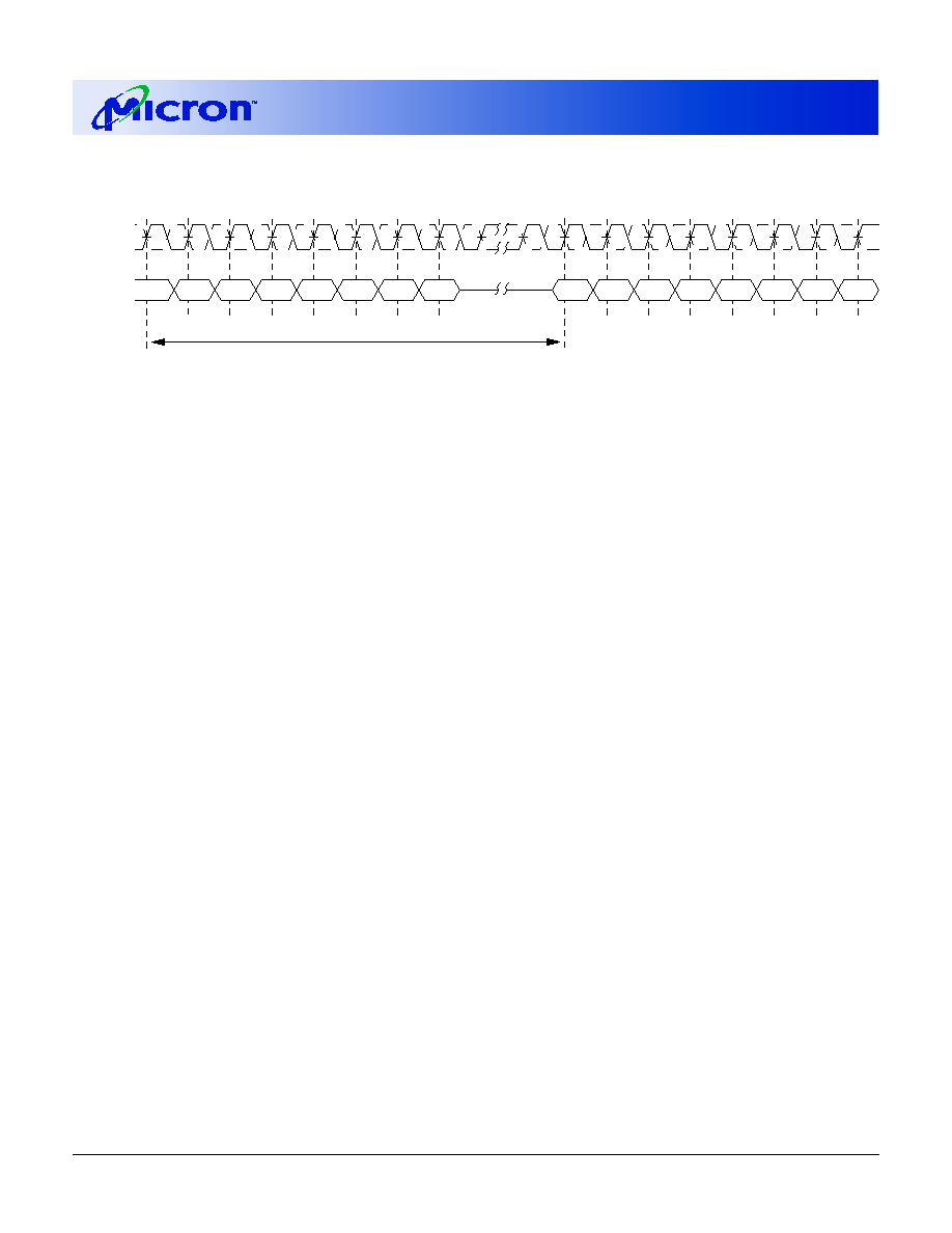
GENERAL OVERVIEW AND TIMING DEFINITION
(BL2/WL2)
NOTE: 1. Address A[19:0] and commands CS#, AS#, WE#, REF# are referenced to the rising edge of the clock CK.
2. Input Data DQ is referenced to the rising or falling edge of the clock.
3. DVLD is referenced to the falling edge of DQS.
CK/CK#
DQS[3:0]#
DQS[3:0]
DVLD
A[19:0]
BA[2:0]
DM[1:0]
WE#
CS#, AS#,
REF#
DQ
1
2
3
4
5
6
7
8
9
tCKH
tCS
tCH
tCKL
tCK
tAS
tAH
tCKDQS
tQSVLD
tQSVLD
tQSQH Z
tQSQ
tDH
tDS
Q0a
Q0b
Q1a
Q1b
D0a
D0b
D1a
D1b
24
256: x16, x32 RLDRAM
Micron Technology, Inc., reserves the right to change products or specifications without notice.
MT49H8M32_3.p65 ≠ Rev. 3, Pub. 6/02
©2002, Micron Technology, Inc.
ADVANCE
256Mb: x16, x32
2.5V V
EXT
, 1.8V V
DD
, 1.8V V
DD
Q, RLDRAM
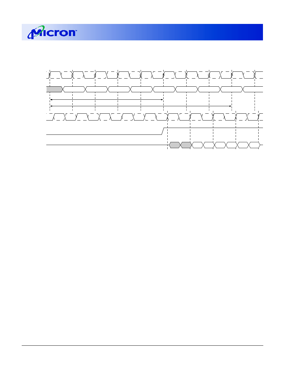
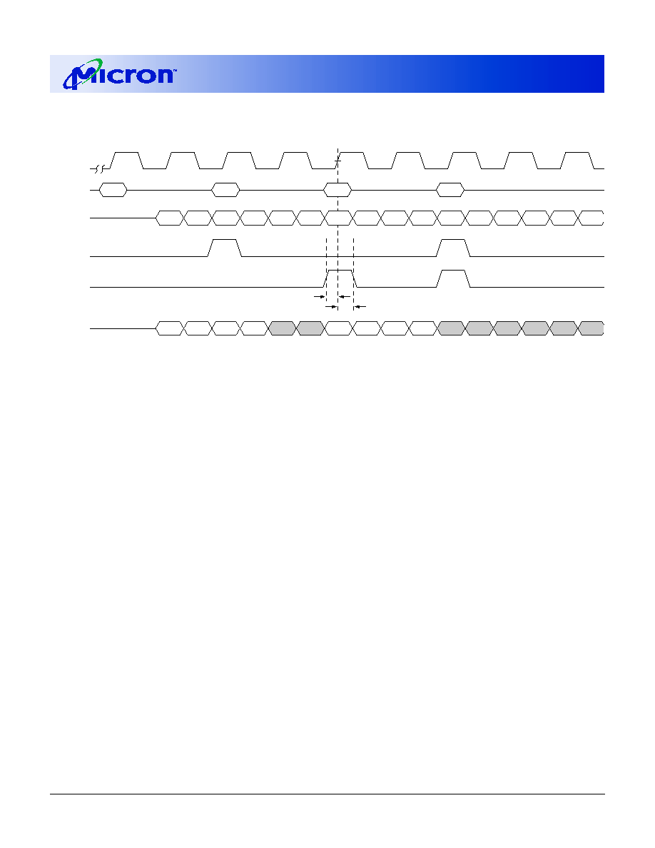
READ TIMING
(BL = 2)
NOTE: 1. Starting with all banks closed, 8 banks cyclic access.
2. 2-bit prefetch, BL = 2.
3. Read latency (RL) programmable.
4. CS# = 1 deactivates command inputs. DQS and DQS# not affected.
CK/CK#
DQS,
DQS#
DVLD
CS#, AS#, REF#
A[19:0], BA[2:0]
DQ
1
2
3
4
5
6
7
8
9
RL = 5 tCK
tRC = 8 tCK
initial
Q0a
Q0b
Q0a
RB0
RB1
RB2
RB3
RB4
RB5
RB6
RB7
RB0
Q1b
Q1a
Q2b
Q2a
Q3b
Q3a

25
256: x16, x32 RLDRAM
Micron Technology, Inc., reserves the right to change products or specifications without notice.
MT49H8M32_3.p65 ≠ Rev. 3, Pub. 6/02
©2002, Micron Technology, Inc.
ADVANCE
256Mb: x16, x32
2.5V V
EXT
, 1.8V V
DD
, 1.8V V
DD
Q, RLDRAM
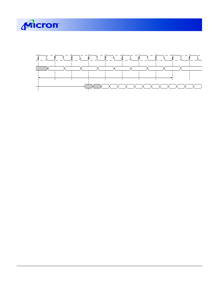
READ TIMING
(BL = 4)
NOTE: 1. Starting with all banks closed, 4 bank cyclic access.
2. 4 bit prefetch, BL = 4.
3. Read latency (RL) programmable.
4. CS# = 1 deactivates command inputs. DQS not affected.
CK/CK#
DQS,
DQS#
DVLD
CS#, AS#, REF#,
A[18:0], BA[2:0]
DQ
1
2
3
4
5
6
7
8
9
RL = 5 tCK
tRC = 8 tCK
initial
Q0a
Q0b
Q0a
RB0
RB1
RB3
RB4
RB0
Q0d
Q0c
Q1b
Q1a
Q1d
Q1c
26
256: x16, x32 RLDRAM
Micron Technology, Inc., reserves the right to change products or specifications without notice.
MT49H8M32_3.p65 ≠ Rev. 3, Pub. 6/02
©2002, Micron Technology, Inc.
ADVANCE
256Mb: x16, x32
2.5V V
EXT
, 1.8V V
DD
, 1.8V V
DD
Q, RLDRAM
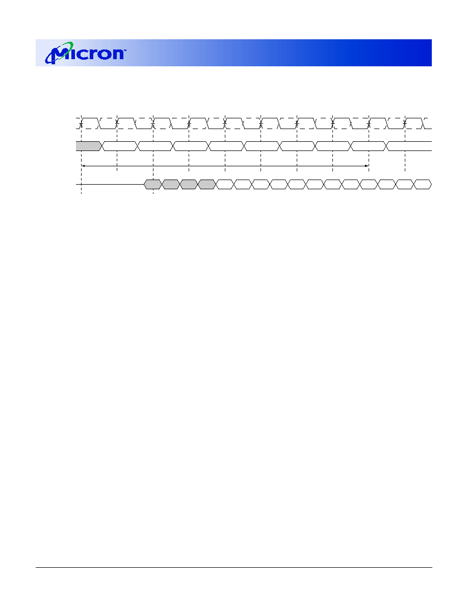
WRITE TIMING
(BL = 2, RL = 6)
NOTE: 1. DQS and DQS# are not relevant during WRITE cycles.
2. Starting with all banks closed, 8 banks cyclic access.
3. Write latency WL = RL - BL/2 - 2 = 3.
CK/CK#
CS#, AS#,
REF#, A[19:0],
BA[2:0], DM[1:0]
DQ
1
2
3
4
5
6
7
8
9
tRC = 8 tCK
D0b
D0a
WB0
WB1
WB2
WB3
WB4
WB5
WB6
WB7
WB0
D1b
D1a
D2b
D2a
D3b
D3a
D4b
D4a
D5b
D5a
D6b
D6a
27
256: x16, x32 RLDRAM
Micron Technology, Inc., reserves the right to change products or specifications without notice.
MT49H8M32_3.p65 ≠ Rev. 3, Pub. 6/02
©2002, Micron Technology, Inc.
ADVANCE
256Mb: x16, x32
2.5V V
EXT
, 1.8V V
DD
, 1.8V V
DD
Q, RLDRAM
WRITE TIMING
(BL = 4, RL = 6)
CK/CK#
CS#, AS#, REF#,
A[18:0], BA[2:0],
DM[1:0]
DQ
1
2
3
4
5
6
7
8
9
tRC = 8 tCK
D0b
D0a
WB0
WB1
WB2
WB3
WB0
D0d
D0c
D1b
D1a
D1d
D1c
D2b
D2a
D2d
D2c
D3d
D3c
D3b
D3a
NOTE: 1. DQS and DQS# are not relevant during WRITE cycles.
2. Starting with all banks closed, 4 banks cyclic access.
3. Write latency WL = RL - BL/2 - 2 = 2.

28
256: x16, x32 RLDRAM
Micron Technology, Inc., reserves the right to change products or specifications without notice.
MT49H8M32_3.p65 ≠ Rev. 3, Pub. 6/02
©2002, Micron Technology, Inc.
ADVANCE
256Mb: x16, x32
2.5V V
EXT
, 1.8V V
DD
, 1.8V V
DD
Q, RLDRAM
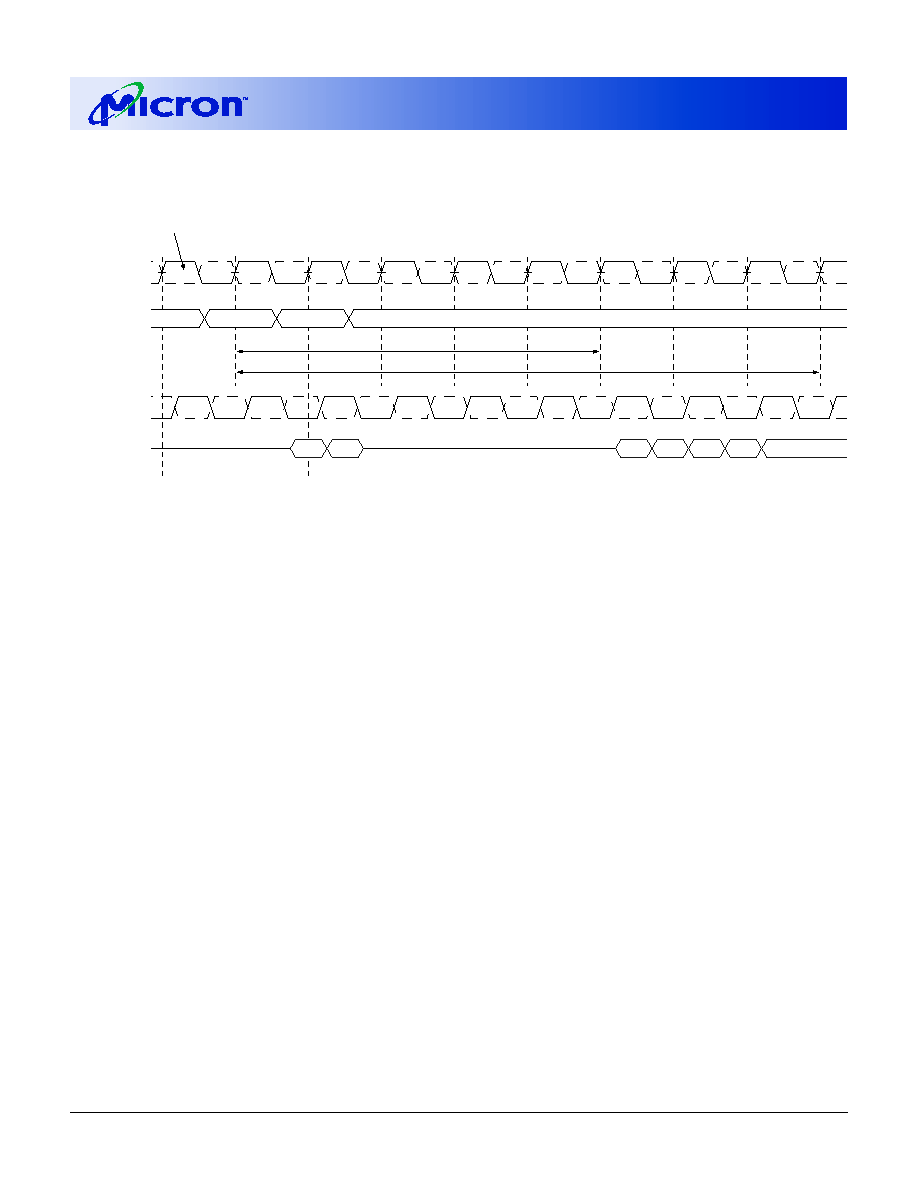
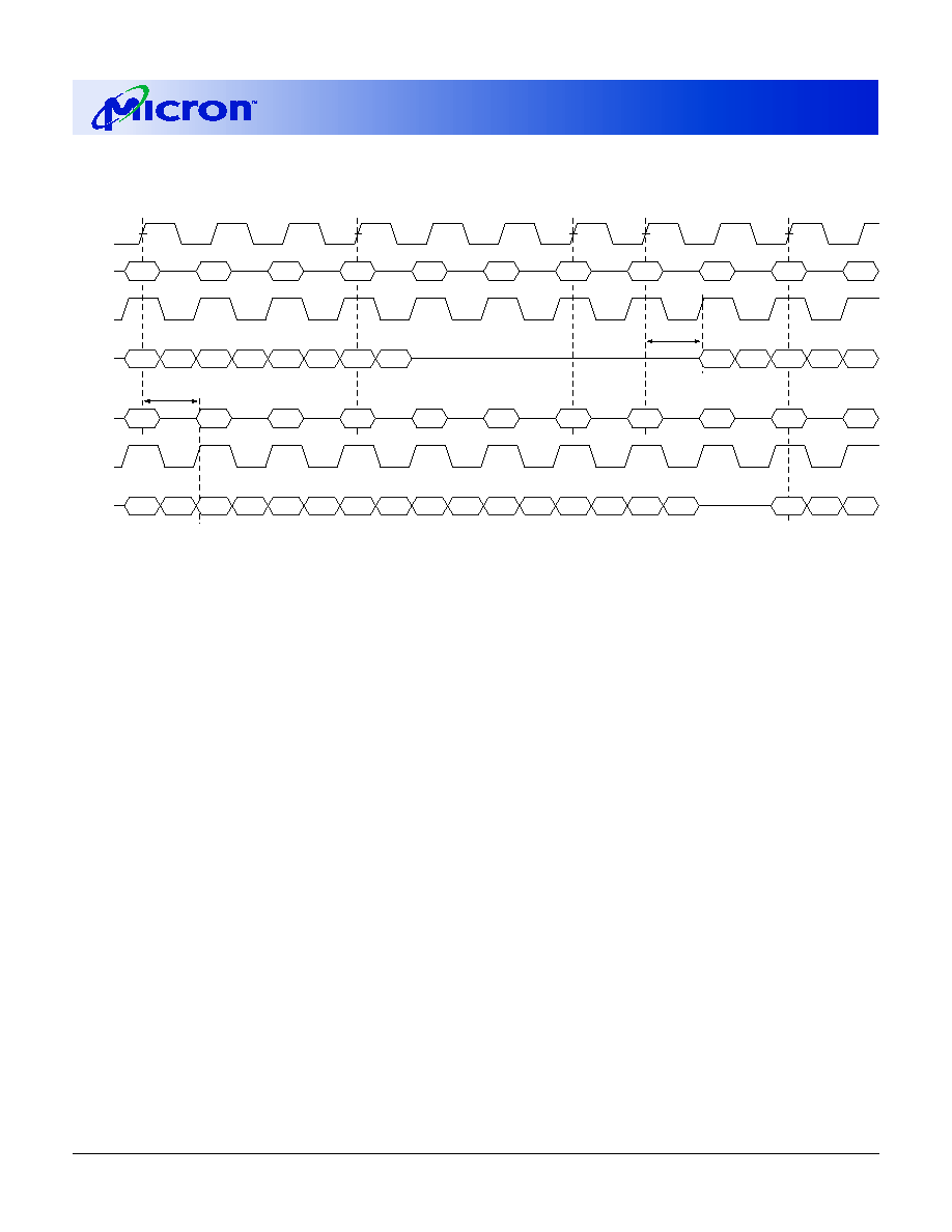
READ TO WRITE TIMING
(BL = 2, WL = 2)
NOTE: 1. In order to avoid bus contention from a READ to a WRITE the proper number of clock cycles has to be inserted.
CK/CK#
DQS,
DQS#
CS#, AS#, REF#,
A[19:0], BA[2:0],
DM[1:0]
DQ
1
2
3
4
5
6
7
8
9
RL = 5 tCK
Last READ
command
Prevent bus
contention
Earliest WRITE
command
Q0b
Q0a
RB3
NOP
NOP
NOP
NOP
WB4
NOP
Q1b
Q1a
Q2b
Q2a
Q3b
Q3a
D4b
D4a
29
256: x16, x32 RLDRAM
Micron Technology, Inc., reserves the right to change products or specifications without notice.
MT49H8M32_3.p65 ≠ Rev. 3, Pub. 6/02
©2002, Micron Technology, Inc.
ADVANCE
256Mb: x16, x32
2.5V V
EXT
, 1.8V V
DD
, 1.8V V
DD
Q, RLDRAM
WRITE TO READ TIMING
(BL = 2, WL = 2)
CK/CK#
DQS,
DQS#
CS#, AS#, REF#,
A[19:0], BA[2:0],
DM[1:0]
DQ
1
2
3
4
5
6
7
8
9
RL = 5 tCK
tRC = 8 tCK
D3b
D3a
WB3
RB4
RB5
Q4a
Q5a
Q4b
Q5b
Last WRITE
command

30
256: x16, x32 RLDRAM
Micron Technology, Inc., reserves the right to change products or specifications without notice.
MT49H8M32_3.p65 ≠ Rev. 3, Pub. 6/02
©2002, Micron Technology, Inc.
ADVANCE
256Mb: x16, x32
2.5V V
EXT
, 1.8V V
DD
, 1.8V V
DD
Q, RLDRAM
REFRESH TIMING
NOTE: 1. Bank scheduled refresh.
2. Refresh cycle to be issued on closed bank.
3. Bank address from controller, row address generated internally.
CK/CK#
DQS,
DQS#
CS#, AS#,
REF#
DQ
RL = 5 tCK
tRC = 8 tCK
tRFC = tRC
Q0
RB5
RB6
RB7
RF0
RB1
RB2
RB3
RB4
RB5
RB6
RB7
RF0
RB1
RB2
RB3
RB4
RB5
Q1
Q3
Q2
Q5
Q4
Q7
Q6
Q1
Q3
Q2
Q5
Q4
Q7
Q6
31
256: x16, x32 RLDRAM
Micron Technology, Inc., reserves the right to change products or specifications without notice.
MT49H8M32_3.p65 ≠ Rev. 3, Pub. 6/02
©2002, Micron Technology, Inc.
ADVANCE
256Mb: x16, x32
2.5V V
EXT
, 1.8V V
DD
, 1.8V V
DD
Q, RLDRAM
EXAMPLE OF REFRESH IMPLEMENTATION
(Cyclic Bank Burst Refresh)
NOTE: 1. Cyclic Burst refresh on all Banks.
2. Each Refresh command on the next Bank is asserted on the next clock rising edge.
3. Cycle for a burst refresh: 32ms/8192 = 3.9µs.
CLK/CLK#
CMD/ADR
RF0
RF1
RF2
RF3
RF4
RF5
RF6
RF7
RF0
RF1
RF2
RF3
RF4
RF5
RF6
RF7
3.9µs

32
256: x16, x32 RLDRAM
Micron Technology, Inc., reserves the right to change products or specifications without notice.
MT49H8M32_3.p65 ≠ Rev. 3, Pub. 6/02
©2002, Micron Technology, Inc.
ADVANCE
256Mb: x16, x32
2.5V V
EXT
, 1.8V V
DD
, 1.8V V
DD
Q, RLDRAM
WRITE DATA MASK TIMING
(BL = 2, WL = 2)
NOTE: 1. Shaded WR Data is not written into the memory.
CK/CK#
DM0
CMD
DM1
WR0
WR1
WR2
WR4
WR3
DQ
D0b
D0a
D1b
D1a
D2b
D2a
D3b
D3a
D4b
D4a
WR DATA
D0b
D0a
D1b
D2a
D4b
D4a
tAS
tAH
33
256: x16, x32 RLDRAM
Micron Technology, Inc., reserves the right to change products or specifications without notice.
MT49H8M32_3.p65 ≠ Rev. 3, Pub. 6/02
©2002, Micron Technology, Inc.
ADVANCE
256Mb: x16, x32
2.5V V
EXT
, 1.8V V
DD
, 1.8V V
DD
Q, RLDRAM
WRITE DATA MASK TIMING
(BL = 4, WL = 1)
NOTE: 1. Shaded WR Data is not written into the memory.
CK/CK#
DM0
CMD
DM1
WR0
WR1
WR3
WR2
DQ
D0b
D0a
D0d
D0c
D1b
D1a
D1d
D1c
D2b
D2a
D2d
D2c
D3b
D3a
D3d
D3c
WR DATA
D0b
D0a
D0d
D2b
D2a
D1d
D1c
tAS
tAH
D0c
34
256: x16, x32 RLDRAM
Micron Technology, Inc., reserves the right to change products or specifications without notice.
MT49H8M32_3.p65 ≠ Rev. 3, Pub. 6/02
©2002, Micron Technology, Inc.
ADVANCE
256Mb: x16, x32
2.5V V
EXT
, 1.8V V
DD
, 1.8V V
DD
Q, RLDRAM
WRITE/READ AND READ/WRITE TIMING, CYCLIC BANK ACCESS
(RL = 6, BL = 2, WL = 3)
CK/CK#
CMD
WB7
RB0
RB1
RB2
RB3
RB4
RB5
RB6
RB7
RB0
RB1
DQS
DQ
D4b
D4a
D5b
D5a
D6b
D6a
Q0b
Q0a
Q1b
Q1a
Q2a
D7b
D7a
tCKDQS
CMD
RB0
NOP
NOP
NOP
NOP
NOP
WB1
WB2
WB3
WB4
WB5
DQS
DQ
Q1b
Q1a
Q2b
Q2a
Q3b
Q3a
D1b
D1a
D2a
Q4b
Q4a
Q5b
Q5a
Q6b
Q6a
Q7b
Q7a
Q7b
Q7a
tCKDQS

35
256: x16, x32 RLDRAM
Micron Technology, Inc., reserves the right to change products or specifications without notice.
MT49H8M32_3.p65 ≠ Rev. 3, Pub. 6/02
©2002, Micron Technology, Inc.
ADVANCE
256Mb: x16, x32
2.5V V
EXT
, 1.8V V
DD
, 1.8V V
DD
Q, RLDRAM
WRITE/READ AND READ/WRITE TIMING, CYCLIC BANK ACCESS
(RL = 5, BL = 2, WL = 2)
CK/CK#
CMD
WB7
RB0
RB1
RB2
RB3
RB4
RB5
RB6
RB7
RB0
RB1
DQS
DQ
D5b
D5a
D6b
D6a
Q0b
Q0a
Q1b
Q1a
Q2a
Q3b
Q3a
D7b
D7a
tCKDQS
CMD
RB0
NOP
NOP
NOP
NOP
NOP
WB1
WB2
WB3
WB4
WB5
DQS
DQ
Q2b
Q2a
Q3b
Q3a
D1b
D1a
D3a
D2b
D2a
Q4b
Q4a
Q5b
Q5a
Q6b
Q6a
Q7b
Q7a
Q0b
Q0a
tCKDQS

36
256: x16, x32 RLDRAM
Micron Technology, Inc., reserves the right to change products or specifications without notice.
MT49H8M32_3.p65 ≠ Rev. 3, Pub. 6/02
©2002, Micron Technology, Inc.
ADVANCE
256Mb: x16, x32
2.5V V
EXT
, 1.8V V
DD
, 1.8V V
DD
Q, RLDRAM
CK/CK#
CMD
WB7
RB0
NOP
RB1
NOP
RB2
NOP
RB3
NOP
RB4
NOP
DQS
DQ
D6b
D6a
D6d
D6c
Q0b
Q0a
Q0d
Q0c
Q1a
D7b
D7a
D7d
D7c
tCKDQS
CMD
RB0
NOP
NOP
NOP
NOP
NOP
NOP
NOP
WB1
NOP
WB2
DQS
DQ
Q4d
Q4c
Q5b
Q5a
D1a
Q5d
Q5c
Q6b
Q6a
Q6d
Q6c
Q7b
Q7a
Q7d
Q7c
Q0b
Q0a
Q0d
Q0c
tCKDQS
WRITE/READ AND READ/WRITE TIMING, CYCLIC BANK ACCESS
(RL = 6, BL = 4, WL = 2)

37
256: x16, x32 RLDRAM
Micron Technology, Inc., reserves the right to change products or specifications without notice.
MT49H8M32_3.p65 ≠ Rev. 3, Pub. 6/02
©2002, Micron Technology, Inc.
ADVANCE
256Mb: x16, x32
2.5V V
EXT
, 1.8V V
DD
, 1.8V V
DD
Q, RLDRAM
CK/CK#
CMD
WB7
RB0
NOP
RB1
NOP
RB2
NOP
RB3
NOP
RB4
NOP
DQS
DQ
D6d
D6c
Q0b
Q0a
Q0d
Q0c
Q1b
Q1c
Q1a
D7b
D7a
D7d
D7c
tCKDQS
CMD
RB0
NOP
NOP
NOP
NOP
NOP
NOP
NOP
WB1
NOP
WB2
DQS
DQ
Q5b
Q5a
D1a
D1b
D1c
Q5d
Q5c
Q6b
Q6a
Q6d
Q6c
Q7b
Q7a
Q7d
Q7c
Q0b
Q0a
Q0d
Q0c
tCKDQS
WRITE/READ AND READ/WRITE TIMING, CYCLIC BANK ACCESS
(RL = 5, BL = 4, WL = 1)
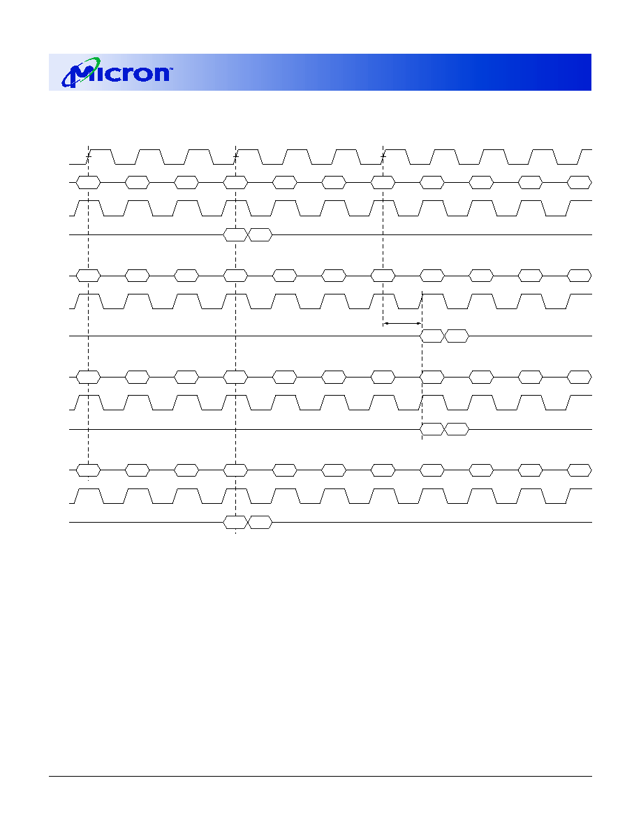
38
256: x16, x32 RLDRAM
Micron Technology, Inc., reserves the right to change products or specifications without notice.
MT49H8M32_3.p65 ≠ Rev. 3, Pub. 6/02
©2002, Micron Technology, Inc.
ADVANCE
256Mb: x16, x32
2.5V V
EXT
, 1.8V V
DD
, 1.8V V
DD
Q, RLDRAM
CK
CMD
WB0
NOP
NOP
NOP
NOP
NOP
NOP
NOP
WB0
NOP
NOP
DQS
DQ
D0b
D0a
D0b
D0a
CMD
RB0
NOP
NOP
NOP
NOP
NOP
NOP
NOP
RB0
NOP
NOP
DQS
DQ
Q0b
Q0a
CMD
RB0
NOP
NOP
NOP
NOP
NOP
NOP
NOP
WB0
NOP
NOP
DQS
DQ
Q0b
Q0a
CMD
WB0
NOP
NOP
NOP
NOP
NOP
NOP
NOP
RB0
NOP
NOP
DQS
DQ
tCKDQS
RANDOM ACCESS, SINGLE BANK
(RL = 6, BL = 2, WL = 3)

39
256: x16, x32 RLDRAM
Micron Technology, Inc., reserves the right to change products or specifications without notice.
MT49H8M32_3.p65 ≠ Rev. 3, Pub. 6/02
©2002, Micron Technology, Inc.
ADVANCE
256Mb: x16, x32
2.5V V
EXT
, 1.8V V
DD
, 1.8V V
DD
Q, RLDRAM
CK
CMD
WB0
NOP
NOP
NOP
NOP
NOP
WB0
NOP
NOP
NOP
NOP
DQS
DQ
D0b
D0a
D0b
D0a
D0b
D0a
D0b
D0a
CMD
RB0
NOP
NOP
NOP
NOP
NOP
RB0
NOP
NOP
NOP
NOP
DQS
DQ
Q0b
Q0a
CMD
RB0
NOP
NOP
NOP
NOP
NOP
WB0
NOP
NOP
NOP
NOP
DQS
DQ
Q0b
Q0a
CMD
WB0
NOP
NOP
NOP
NOP
NOP
RB0
NOP
NOP
NOP
NOP
DQS
DQ
tCKDQS
RANDOM ACCESS, SINGLE BANK
(RL = 5, BL = 2, WL = 2,
t
RC = 6)

40
256: x16, x32 RLDRAM
Micron Technology, Inc., reserves the right to change products or specifications without notice.
MT49H8M32_3.p65 ≠ Rev. 3, Pub. 6/02
©2002, Micron Technology, Inc.
ADVANCE
256Mb: x16, x32
2.5V V
EXT
, 1.8V V
DD
, 1.8V V
DD
Q, RLDRAM
CK
CMD
WB0
NOP
NOP
NOP
NOP
NOP
NOP
NOP
WB0
NOP
NOP
DQS
DQ
D0b
D0a
D0d
D0c
D0a
Q0d
D0a
Q0c
D0b
D0a
D0d
D0c
CMD
RB0
NOP
NOP
NOP
NOP
NOP
NOP
NOP
RB0
NOP
NOP
DQS
DQ
Q0b
Q0a
Q0d
Q0c
CMD
RB0
NOP
NOP
NOP
NOP
NOP
NOP
NOP
WB0
NOP
NOP
DQS
DQ
Q0b
Q0a
CMD
WB0
NOP
NOP
NOP
NOP
NOP
NOP
NOP
RB0
NOP
NOP
DQS
DQ
tCKDQS
RANDOM ACCESS, SINGLE BANK
(RL = 6, BL = 4, WL = 2)

41
256: x16, x32 RLDRAM
Micron Technology, Inc., reserves the right to change products or specifications without notice.
MT49H8M32_3.p65 ≠ Rev. 3, Pub. 6/02
©2002, Micron Technology, Inc.
ADVANCE
256Mb: x16, x32
2.5V V
EXT
, 1.8V V
DD
, 1.8V V
DD
Q, RLDRAM
CK
CMD
WB0
NOP
NOP
NOP
NOP
NOP
WB0
NOP
NOP
NOP
NOP
DQS
DQ
D0b
D0a
D0d
D0c
D0b
D0a
D0d
D0c
Q0d
D0a
D0b
D0c
Q0c
D0b
D0a
D0d
D0c
CMD
RB0
NOP
NOP
NOP
NOP
NOP
RB0
NOP
NOP
NOP
NOP
DQS
DQ
Q0b
Q0a
Q0d
Q0c
CMD
RB0
NOP
NOP
NOP
NOP
NOP
NOP
NOP
WB0
NOP
NOP
DQS
DQ
Q0b
Q0a
CMD
WB0
NOP
NOP
NOP
NOP
NOP
RB0
NOP
NOP
NOP
NOP
DQS
DQ
tCKDQS
RANDOM ACCESS, SINGLE BANK
(RL = 5, BL = 4, WL = 1,
t
RC = 6)

42
256: x16, x32 RLDRAM
Micron Technology, Inc., reserves the right to change products or specifications without notice.
MT49H8M32_3.p65 ≠ Rev. 3, Pub. 6/02
©2002, Micron Technology, Inc.
ADVANCE
256Mb: x16, x32
2.5V V
EXT
, 1.8V V
DD
, 1.8V V
DD
Q, RLDRAM
8000 S. Federal Way, P.O. Box 6, Boise, ID 83707-0006, Tel: 208-368-3900
E-mail: prodmktg@micron.com, Internet: http://www.micron.com, Customer Comment Line: 800-932-4992
Micron and the M logo are registered trademarks and the Micron logo is a trademark of Micron Technology, Inc.
DATA SHEET DESIGNATION
Advance:
This data sheet contains initial descriptions of products still under development.
144-BALL T-FBGA
SEATING PLANE
0.850 ±0.075
0.155 ±0.013
0.10 C
C
PIN A1 ID
PIN A1 ID
BALL A1
MOLD COMPOUND: EPOXY NOVOLAC
SUBSTRATE: PLASTIC LAMINATE
1.20 MAX
SOLDER BALL MATERIAL: EUTECTIC 63% Sn, 37% Pb or
62% Sn, 37% Pb, 2%Ag
SOLDER BALL PAD: ÿ .33mm
18.50 ±0.10
17.00
1.00
(TYP)
4.40 ±0.05
11.00 ±0.10
5.50 ±0.05
8.50 ±0.05
9.25 ±0.05
TYP
BALL A12
144X .45
ÿ
SOLDER BALL DIAMETER
REFERS TO POST REFLOW
CONDITION. THE
PRE-REFLOW DIAMETER
IS ÿ 0.40
C
L
C
L
8.80
2.20 ±0.05
CTR
0.80
(TYP)
NOTE: 1. All dimensions in millimeters.

43
256: x16, x32 RLDRAM
Micron Technology, Inc., reserves the right to change products or specifications without notice.
MT49H8M32_3.p65 ≠ Rev. 3, Pub. 6/02
©2002, Micron Technology, Inc.
ADVANCE
256Mb: x16, x32
2.5V V
EXT
, 1.8V V
DD
, 1.8V V
DD
Q, RLDRAM
REVISION HISTORY
Rev. 3, Advance ................................................................................................................................................................... 6/02
∑ Removed confidential mark
Rev. 2, Advance ................................................................................................................................................................... 2/02
∑ ?
∑ ?
Original document, Advance .......................................................................................................................................... 12/01