Document Outline
- Features
- Options
- Key Timing Parameters
- Pin Assignment
- 16 Meg x 4 EDO DRAM Part Numbers
- General Description
- Functional Block Diagrams
- MT4LC16M4G3 (13 row addresses)
- MT4LC16M4H9 (12 row addresses)
- DRAM Access
- EDO Page Mode
- DRAM Refresh
- Standby
- Figure 1 OE# Control of DQs
- Figure 2 WE# Control of DQs
- Absolute Maximum Ratings
- DC Electrical Characteristics and Operating Conditions
- ICC Operating Conditions and Maximum Limits
- Capacitance
- AC Electrical Characteristics
- AC Electrical Characteristics
- Notes
- READ Cycle
- EARLY WRITE Cycle
- READ-WRITE Cycle
- EDO-PAGE-MODE READ Cycle
- EDO-PAGE-MODE EARLY WRITE Cycle
- EDO-PAGE-MODE READ-WRITE Cycle
- EDO-PAGE-MODE READ EARLY WRITE Cycle
- READ Cycle
- RAS#-ONLY REFRESH Cycle
- HIDDEN REFRESH Cycle
- SELF REFRESH Cycle
- 32-Pin Plastic SOJ (400 mil)
- 32-Pin Plastic TSOP (400 mil)
1
16 Meg x 4 EDO DRAM
Micron Technology, Inc., reserves the right to change products or specifications without notice.
D22_2.p65 ≠ Rev. 5/00
©2000, Micron Technology, Inc.
16 MEG x 4
EDO DRAM
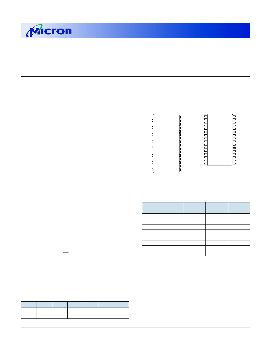
16 MEG x 4 EDO DRAM PART NUMBERS
REFRESH
PART NUMBER
ADDRESSING
PACKAGE
REFRESH
MT4LC16M4H9DJ-x
4K
SOJ
Standard
MT4LC16M4H9DJ-x S
4K
SOJ
Self
MT4LC16M4H9TG-x
4K
TSOP
Standard
MT4LC16M4H9TG-x S
4K
TSOP
Self
MT4LC16M4G3DJ-x
8K
SOJ
Standard
MT4LC16M4G3DJ-x S
8K
SOJ
Self
MT4LC16M4G3TG-x
8K
TSOP
Standard
MT4LC16M4G3TG-x S
8K
TSOP
Self
x = speed
FEATURES
∑ Single +3.3V ±0.3V power supply
∑ Industry-standard x4 pinout, timing, functions,
and packages
∑ 12 row, 12 column addresses (H9) or
13 row, 11 column addresses (G3)
∑ High-performance CMOS silicon-gate process
∑ All inputs, outputs and clocks are LVTTL-compat-
ible
∑ Extended Data-Out (EDO) PAGE MODE access
∑ Optional self refresh (S) for low-power data
retention
∑ 4,096-cycle CAS#-BEFORE-RAS# (CBR) REFRESH
distributed across 64ms
OPTIONS
MARKING
∑ Refresh Addressing
4,096 (4K) rows
H9
8,192 (8K) rows
G3
∑ Plastic Packages
32-pin SOJ (400 mil)
DJ
32-pin TSOP (400 mil)
TG
∑ Timing
50ns access
-5
60ns access
-6
∑ Refresh Rates
Standard Refresh
None
Self Refresh (128ms period)
S*
NOTE: 1. The 16 Meg x 4 EDO DRAM base number
differentiates the offerings in one place--
MT4LC16M4H9. The fifth field distinguishes the
address offerings: H9 designates 4K addresses and
G3 designates 8K addresses.
2. The "#" symbol indicates signal is active LOW.
*Contact factory for availability
Part Number Example:
MT4LC16M4H9DJ-6
PIN ASSIGNMENT (Top View)
DRAM
MT4LC16M4G3, MT4LC16M4H9
For the latest data sheet, please refer to the Micron Web
site:
www.micronsemi.com/mti/msp/html/datasheet.html
32-Pin SOJ
32-Pin TSOP
V
CC
DQ0
DQ1
NC
NC
NC
NC
WE#
RAS#
A0
A1
A2
A3
A4
A5
V
CC
1
2
3
4
5
6
7
8
9
10
11
12
13
14
15
16
32
31
30
29
28
27
26
25
24
23
22
21
20
19
18
17
Vss
DQ3
DQ2
NC
NC
NC
CAS#
OE#
NC/
A12
**
A11
A10
A9
A8
A7
A6
Vss
V
CC
DQ0
DQ1
NC
NC
NC
NC
WE#
RAS#
A0
A1
A2
A3
A4
A5
V
CC
1
2
3
4
5
6
7
8
9
10
11
12
13
14
15
16
32
31
30
29
28
27
26
25
24
23
22
21
20
19
18
17
Vss
DQ3
DQ2
NC
NC
NC
CAS#
OE#
NC/
A12
**
A11
A10
A9
A8
A7
A6
Vss
KEY TIMING PARAMETERS
SPEED
t
RC
t
RAC
t
PC
t
AA
t
CAC
t
CAS
-5
84ns
50ns
20ns
25ns
13ns
8ns
-6
104ns
60ns
25ns
30ns
15ns
10ns
**NC on H9 version, A12 on G3 version
GENERAL DESCRIPTION
The 16 Meg x 4 DRAM is a high-speed CMOS,
dynamic random-access memory device containing
67,108,864 bits and designed to operate from 3V to
3.6V. The MT4LC16M4H9 and MT4LC16M4G3 are
functionally organized as 16,777,216 locations con-
taining 4 bits each. The 16,777,216 memory locations
are arranged in 4,096 rows by 4,096 columns on the H9
version and 8,192 rows by 2,048 columns on the G3
version. During READ or WRITE cycles, each location is
2
16 Meg x 4 EDO DRAM
Micron Technology, Inc., reserves the right to change products or specifications without notice.
D22_2.p65 ≠ Rev. 5/00
©2000, Micron Technology, Inc.
16 MEG x 4
EDO DRAM
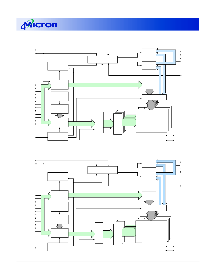
FUNCTIONAL BLOCK DIAGRAM
MT4LC16M4G3 (13 row addresses)
A0
A1
A2
A3
A4
A5
A6
A7
A8
A9
A10
A11
A12
RAS#
13
13
11
NO. 2 CLOCK
GENERATOR
REFRESH
CONTROLLER
NO. 1 CLOCK
GENERATOR
V
DD
V
SS
13
WE#
CAS#
11
CONTROL
LOGIC
COLUMN-
ADDRESS
BUFFER(11)
ROW-
ADDRESS
BUFFERS (13)
8,192
2,048
COLUMN
DECODER
OE#
DQ0
DQ1
DQ2
DQ3
4
4
4
4
REFRESH
COUNTER
ROW SELECT
ROW
DECODER
2,048
SENSE AMPLIFIERS
I/O GATING
DATA-OUT
BUFFER
DATA-IN
BUFFER
8,192 x 2,048 x 4
MEMORY
ARRAY
COMPLEMENT
SELECT
8,192
FUNCTIONAL BLOCK DIAGRAM
MT4LC16M4H9 (12 row addresses)
A0
A1
A2
A3
A4
A5
A6
A7
A8
A9
A10
A11
RAS#
12
12
12
NO. 2 CLOCK
GENERATOR
REFRESH
CONTROLLER
NO. 1 CLOCK
GENERATOR
V
DD
V
SS
12
WE#
CAS#
12
CONTROL
LOGIC
COLUMN-
ADDRESS
BUFFER(12)
ROW-
ADDRESS
BUFFERS (12)
4,096
4,096
COLUMN
DECODER
OE#
DQ0
DQ1
DQ2
DQ3
4
4
4
4
REFRESH
COUNTER
ROW SELECT
ROW
DECODER
4,096
SENSE AMPLIFIERS
I/O GATING
DATA-OUT
BUFFER
DATA-IN
BUFFER
4,096 x 4,096 x 4
MEMORY
ARRAY
COMPLEMENT
SELECT
4,096

3
16 Meg x 4 EDO DRAM
Micron Technology, Inc., reserves the right to change products or specifications without notice.
D22_2.p65 ≠ Rev. 5/00
©2000, Micron Technology, Inc.
16 MEG x 4
EDO DRAM
uniquely addressed via the address bits. First, the row
address is latched by the RAS# signal, then the column
address is latched by CAS#. The device provides EDO-
PAGE-MODE operation, allowing for fast successive
data operations (READ, WRITE, or READ-MODIFY-
WRITE) within a given row.
The 16 Meg x 4 DRAM must be refreshed periodically
in order to retain stored data.
DRAM ACCESS
Each location in the DRAM is uniquely addressable,
as mentioned in the General Description. The data for
each location is accessed via the four I/O pins (DQ0-
DQ3). A logic HIGH on WE# dictates read mode, while
a logic LOW on WE# dictates write mode. During a
WRITE cycle, data-in (D) is latched by the falling edge
of WE# or CAS#, whichever occurs last. An EARLY
WRITE occurs when WE# is taken LOW prior to CAS#
falling. A LATE WRITE or READ-MODIFY-WRITE occurs
when WE# falls after CAS# is taken LOW. During
EARLY WRITE cycles, the data outputs (Q) will remain
High-Z, regardless of the state of OE#. During LATE
WRITE or READ-MODIFY-WRITE cycles, OE# must be
taken HIGH to disable the data outputs prior to apply-
ing input data. If a LATE WRITE or READ-MODIFY-
WRITE is attempted while keeping OE# LOW, no WRITE
will occur, and the data outputs will drive read data
from the accessed location.
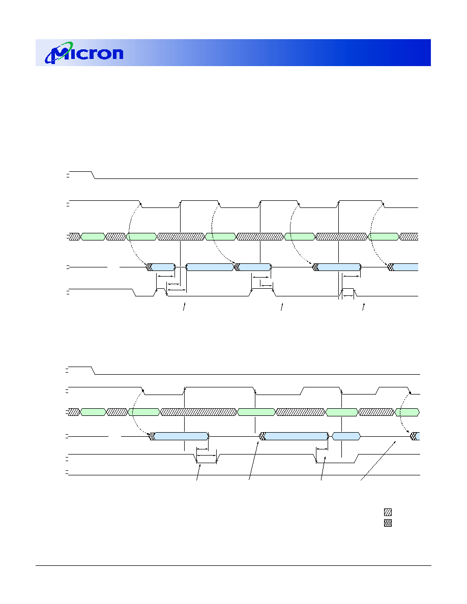
EDO PAGE MODE
DRAM READ cycles have traditionally turned the
output buffers off (High-Z) with the rising edge of
CAS#. If CAS# went HIGH and OE# was LOW (active),
the output buffers would be disabled. The 16 Meg x 4
DRAM offers an accelerated page mode cycle by elimi-
nating output disable from CAS# HIGH. This option is
called EDO and it allows CAS# precharge time (
t
CP) to
occur without the output data going invalid (see READ
and EDO-PAGE-MODE READ waveforms).
EDO operates like any DRAM READ or FAST-PAGE-
MODE READ, except data is held valid after CAS# goes
HIGH, as long as RAS# and OE# are held LOW and WE#
is held HIGH. OE# can be brought LOW or HIGH while
CAS# and RAS# are LOW, and the DQs will transition
between valid data and High-Z. Using OE#, there are
two methods to disable the outputs and keep them
disabled during the CAS# HIGH time. The first method
is to have OE# HIGH when CAS# transitions HIGH and
keep OE# HIGH for
t
OEHC thereafter. This will disable
the DQs, and they will remain disabled (regardless of
the state of OE# after that point) until CAS# falls again.
The second method is to have OE# LOW when CAS#
transitions HIGH and then bring OE# HIGH for a
minimum of
t
OEP anytime during the CAS# HIGH
period. This will disable the DQs, and they will remain
disabled (regardless of the state of OE# after that point)
until CAS# falls again. (Please refer to Figure 1.) During
other cycles, the outputs are disabled at
t
OFF time after
RAS# and CAS# are HIGH or at
t
WHZ after WE# transi-
tions LOW. The
t
OFF time is referenced from the rising
edge of RAS# or CAS#, whichever occurs last. WE# can
also perform the function of disabling the output
drivers under certain conditions, as shown in Figure 2.
EDO-PAGE-MODE operations are always initiated
with a row address strobed in by the RAS# signal,
followed by a column address strobed in by CAS#, just
like for single location accesses. However, subsequent
column locations within the row may then be accessed
at the page mode cycle time. This is accomplished by
cycling CAS# while holding RAS# LOW and entering
new column addresses with each CAS# cycle. Returning
RAS# HIGH terminates the EDO-PAGE-MODE opera-
tion.
DRAM REFRESH
The supply voltage must be maintained at the speci-
fied levels, and the refresh requirements must be met in
order to retain stored data in the DRAM. The refresh
requirements are met by refreshing all 8,192 rows (G3)
or all 4,096 rows (H9) in the DRAM array at least once
every 64ms. The recommended procedure is to execute
4,096 CBR REFRESH cycles, either uniformly spaced or
grouped in bursts, every 64ms. The MT4LC16M4G3
internally refreshes two rows for every CBR cycle,
whereas the MT4LC16M4H9 refreshes one row for
every CBR cycle. So with either device, executing 4,096
CBR cycles covers all rows. The CBR refresh will invoke
the internal refresh counter for automatic RAS# ad-
dressing. Alternatively, RAS#-ONLY REFRESH capabil-
ity is inherently provided. However, with this method,
some compatibility issues may become apparent. For
example, both G3 and H9 versions require 4,096 CBR
REFRESH cycles, yet each requires a different number of
RAS#-ONLY REFRESH cycles (G3 = 8,192 and H9 =
4,096). JEDEC strongly recommends the use of CBR
REFRESH for this device.
An optional self refresh mode is also available on the
"S" version. The self refresh feature is initiated by
performing a CBR REFRESH cycle and holding RAS#
LOW for the specified
t
RASS. The "S" option allows for
an extended refresh period of 128ms, or 31.25µs per
row for a 4K refresh and 15.625µs per row for an 8K
refresh, when using a distributed CBR REFRESH. This
refresh rate can be applied during normal operation, as
well as during a standby or battery backup mode.
GENERAL DESCRIPTION (Continued)
4
16 Meg x 4 EDO DRAM
Micron Technology, Inc., reserves the right to change products or specifications without notice.
D22_2.p65 ≠ Rev. 5/00
©2000, Micron Technology, Inc.
16 MEG x 4
EDO DRAM
V
V
IH
IL
CAS#
V
V
IH
IL
RAS#
V
V
IH
IL
ADDR
ROW
COLUMN (A)
DON'T CARE
UNDEFINED
V
V
IH
IL
WE#
V
V
IOH
IOL
OPEN
DQ
tWPZ
The DQs go to High-Z if WE# falls and, if
t
WPZ is met,
will remain High-Z until CAS# goes LOW with
WE# HIGH (i.e., until a READ cycle is initiated).
V
V
IH
IL
OE#
VALID DATA (B)
t
WHZ
WE# may be used to disable the DQs to prepare
for input data in an EARLY WRITE cycle. The DQs
will remain High-Z until CAS# goes LOW with
WE# HIGH (i.e., until a READ cycle is initiated).
t
WHZ
COLUMN (D)
VALID DATA (A)
COLUMN (B)
COLUMN (C)
INPUT DATA (C)
Figure 2
WE# Control of DQs
V
V
IH
IL
CAS#
V
V
IH
IL
RAS#
V
V
IH
IL
ADDR
ROW
COLUMN (A)
COLUMN (B)
V
V
IH
IL
OE#
V
V
IOH
IOL
OPEN
DQ
tOD
VALID DATA (B)
VALID DATA (A)
COLUMN (C)
VALID DATA (A)
tOE
VALID DATA (C)
COLUMN (D)
VALID DATA (D)
tOD
tOEHC
tOD
tOEP
tOES
The DQs go back to
Low-Z if
t
OES is met.
The DQs remain High-Z
until the next CAS# cycle
if
t
OEHC is met.
The DQs remain High-Z
until the next CAS# cycle
if
t
OEP is met.
Figure 1
OE# Control of DQs
The self refresh mode is terminated by driving RAS#
HIGH for a minimum time of
t
RPS. This delay allows for
the completion of any internal refresh cycles that may
be in process at the time of the RAS# LOW-to-HIGH
transition. If the DRAM controller uses a distributed
CBR refresh sequence, a burst refresh is not required
upon exiting self refresh. However, if the DRAM con-
troller uses RAS#-ONLY or burst CBR refresh, all rows
must be refreshed with a refresh rate of
t
RC minimum
prior to resuming normal operation.
STANDBY
Returning RAS# and CAS# HIGH terminates a
memory cycle and decreases chip current to a reduced
standby level. The chip is preconditioned for the next
cycle during the RAS# HIGH time.
DRAM REFRESH (Continued)

5
16 Meg x 4 EDO DRAM
Micron Technology, Inc., reserves the right to change products or specifications without notice.
D22_2.p65 ≠ Rev. 5/00
©2000, Micron Technology, Inc.
16 MEG x 4
EDO DRAM
ABSOLUTE MAXIMUM RATINGS*
Voltage on V
CC
Relative to V
SS
................ -1V to +4.6V
Voltage on NC, Inputs or I/O Pins
Relative to V
SS
....................................... -1V to +4.6V
Operating Temperature, T
A
(ambient) ... 0∞C to +70∞C
Storage Temperature (plastic) ............ -55∞C to +150∞C
Power Dissipation ................................................... 1W
*Stresses greater than those listed under "Absolute
Maximum Ratings" may cause permanent damage to
the device. This is a stress rating only, and functional
operation of the device at these or any other conditions
above those indicated in the operational sections of
this specification is not implied. Exposure to absolute
maximum rating conditions for extended periods may
affect reliability.
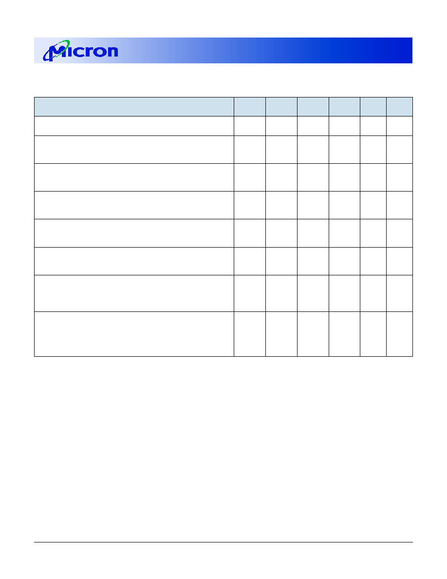
DC ELECTRICAL CHARACTERISTICS AND OPERATING CONDITIONS
(Note: 1) (V
CC
= +3.3V ±0.3V)
PARAMETER/CONDITION
SYMBOL
MIN
MAX
UNITS NOTES
SUPPLY VOLTAGE
V
CC
3
3.6
V
INPUT HIGH VOLTAGE:
Valid Logic 1; All inputs, I/Os and any NC
V
IH
2
V
CC
+ 0.3
V
26
INPUT LOW VOLTAGE:
Valid Logic 0; All inputs, I/Os and any NC
V
IL
-0.3
0.8
V
26
INPUT LEAKAGE CURRENT:
Any input at V
IN
(0V
V
IN
V
CC
+ 0.3V);
I
I
-2
2
µA
27
All other pins not under test = 0V
OUTPUT HIGH VOLTAGE:
I
OUT
= -2mA
V
OH
2.4
≠
V
OUTPUT LOW VOLTAGE:
I
OUT
= 2mA
V
OL
≠
0.4
V
OUTPUT LEAKAGE CURRENT:
Any output at V
OUT
(0V
V
OUT
V
CC
+ 0.3V);
I
OZ
-5
5
µA
DQ is disabled and in High-Z state
6
16 Meg x 4 EDO DRAM
Micron Technology, Inc., reserves the right to change products or specifications without notice.
D22_2.p65 ≠ Rev. 5/00
©2000, Micron Technology, Inc.
16 MEG x 4
EDO DRAM
ICC OPERATING CONDITIONS AND MAXIMUM LIMITS
(Notes: 1, 2, 3, 5, 6) (V
CC
= +3.3V ±0.3V)
4K
8K
PARAMETER/CONDITION
SYMBOL
SPEED
REFRESH REFRESH UNITS NOTES
STANDBY CURRENT: TTL
I
CC
1
ALL
1
1
mA
(RAS# = CAS# = V
IH
)
STANDBY CURRENT: CMOS
(RAS# = CAS#
V
CC
- 0.2V; DQs may be left open;
I
CC
2
ALL
500
500
µA
Other inputs: V
IN
V
CC
- 0.2V or V
IN
0.2V)
OPERATING CURRENT: Random READ/WRITE
I
CC
3
-5
170
130
mA
25
Average power supply current
-6
160
120
(RAS#, CAS#, address cycling:
t
RC =
t
RC [MIN])
OPERATING CURRENT: EDO PAGE MODE
I
CC
4
-5
150
150
mA
25
Average power supply current
-6
120
120
(RAS# = V
IL
, CAS#, address cycling:
t
PC =
t
PC [MIN])
REFRESH CURRENT: RAS#-ONLY
I
CC
5
-5
170
130
mA
22
Average power supply current
-6
160
120
(RAS# cycling, CAS# = V
IH
:
t
RC =
t
RC [MIN])
REFRESH CURRENT: CBR
I
CC
6
-5
160
160
mA
4, 7
Average power supply current
-6
150
150
(RAS#, CAS#, address cycling:
t
RC =
t
RC [MIN])
REFRESH CURRENT: Extended ("S" version only)
Average power supply current: CAS# = 0.2V or CBR cycling;
I
CC
7
ALL
400
400
µA
4, 7
RAS# =
t
RAS (MIN); WE# = V
CC
- 0.2V; A0-A11, OE# and
D
IN
= V
CC
- 0.2V or 0.2V (D
IN
may be left open)
REFRESH CURRENT: Self ("S" version only)
Average power supply current: CBR with
RAS#
t
RASS (MIN) and CAS# held LOW;
I
CC
8
ALL
400
400
µA
4, 7
WE# = V
CC
- 0.2V; A0-A11, OE# and D
IN
= V
CC
- 0.2V or 0.2V
(D
IN
may be left open)
7
16 Meg x 4 EDO DRAM
Micron Technology, Inc., reserves the right to change products or specifications without notice.
D22_2.p65 ≠ Rev. 5/00
©2000, Micron Technology, Inc.
16 MEG x 4
EDO DRAM
CAPACITANCE
(Note: 2)
PARAMETER
SYMBOL
MAX
UNITS
Input Capacitance: Address pins
C
I
1
5
pF
Input Capacitance: RAS#, CAS#, WE#, OE#
C
I
2
7
pF
Input/Output Capacitance: DQ
C
IO
7
pF
AC ELECTRICAL CHARACTERISTICS
(Notes: 5, 6, 7, 8, 9, 10, 11, 12) (V
CC
= +3.3V ±0.3V)
AC CHARACTERISTICS
-5
-6
PARAMETER
SYMBOL
MIN
MAX
MIN
MAX
UNITS
NOTES
Access time from column address
t
AA
25
30
ns
Column-address setup to CAS# precharge
t
ACH
12
15
ns
Column-address hold time (referenced to RAS#)
t
AR
38
45
ns
Column-address setup time
t
ASC
0
0
ns
Row-address setup time
t
ASR
0
0
ns
Column address to WE# delay time
t
AWD
42
49
ns
18
Access time from CAS#
t
CAC
13
15
ns
Column-address hold time
t
CAH
8
10
ns
CAS# pulse width
t
CAS
8
10,000
10
10,000
ns
CAS# LOW to "Don't Care" during Self Refresh
t
CHD
15
15
ns
CAS# hold time (CBR Refresh)
t
CHR
8
10
ns
4
CAS# to output in Low-Z
t
CLZ
0
0
ns
Data output hold after CAS# LOW
t
COH
3
3
ns
CAS# precharge time
t
CP
8
10
ns
13
Access time from CAS# precharge
t
CPA
28
35
ns
CAS# to RAS# precharge time
t
CRP
5
5
ns
CAS# hold time
t
CSH
38
45
ns
CAS# setup time (CBR Refresh)
t
CSR
5
5
ns
4
CAS# to WE# delay time
t
CWD
28
35
ns
18
WRITE command to CAS# lead time
t
CWL
8
10
ns
Data-in hold time
t
DH
8
10
ns
19
Data-in setup time
t
DS
0
0
ns
19
Output disable
t
OD
0
12
0
15
ns
23, 24
Output enable time
t
OE
12
15
ns
20
OE# hold time from WE# during
t
OEH
8
10
ns
24
READ-MODIFY-WRITE cycle
OE# HIGH hold time from CAS# HIGH
t
OEHC
5
10
ns
OE# HIGH pulse width
t
OEP
5
5
ns
OE# LOW to CAS# HIGH setup time
t
OES
4
5
ns
Output buffer turn-off delay
t
OFF
0
12
0
15
ns
17, 23

8
16 Meg x 4 EDO DRAM
Micron Technology, Inc., reserves the right to change products or specifications without notice.
D22_2.p65 ≠ Rev. 5/00
©2000, Micron Technology, Inc.
16 MEG x 4
EDO DRAM
AC ELECTRICAL CHARACTERISTICS
(Notes: 5, 6, 7, 8, 9, 10, 11, 12) (V
CC
= +3.3V ±0.3V)
AC CHARACTERISTICS
-5
-6
PARAMETER
SYMBOL
MIN
MAX
MIN
MAX
UNITS
NOTES
OE# setup prior to RAS# during
t
ORD
0
0
ns
HIDDEN REFRESH cycle
EDO-PAGE-MODE READ or WRITE cycle time
t
PC
20
25
ns
EDO-PAGE-MODE READ-WRITE cycle time
t
PRWC
47
56
ns
Access time from RAS#
t
RAC
50
60
ns
23
RAS# to column-address delay time
t
RAD
9
12
ns
15
Row-address hold time
t
RAH
9
10
ns
RAS# pulse width
t
RAS
50
10,000
60
10,000
ns
RAS# pulse width (EDO PAGE MODE)
t
RASP
50
125,000
60
125,000
ns
RAS# pulse width during Self Refresh
t
RASS
100
100
µs
Random READ or WRITE cycle time
t
RC
84
104
ns
RAS# to CAS# delay time
t
RCD
11
14
ns
14
READ command hold time (referenced to CAS#)
t
RCH
0
0
ns
16
READ command setup time
t
RCS
0
0
ns
Refresh period
t
REF
64
64
ms
22
Refresh period (4,096 cycles) "S" version
t
REF
128
128
ms
4
RAS# precharge time
t
RP
30
40
ns
RAS# to CAS# precharge time
t
RPC
5
5
ns
RAS# precharge time exiting Self Refresh
t
RPS
90
105
ns
READ command hold time (referenced to RAS#)
t
RRH
0
0
ns
16
RAS# hold time
t
RSH
13
15
ns
READ-WRITE cycle time
t
RWC
116
140
ns
RAS# to WE# delay time
t
RWD
67
79
ns
18
WRITE command to RAS# lead time
t
RWL
13
15
ns
Transition time (rise or fall)
t
T
2
50
2
50
ns
WRITE command hold time
t
WCH
8
10
ns
WRITE command hold time (referenced to RAS#)
t
WCR
38
45
ns
WE# command setup time
t
WCS
0
0
ns
18
WE# to outputs in High-Z
t
WHZ
0
12
0
15
ns
WRITE command pulse width
t
WP
5
5
ns
WE# pulse width to disable outputs
t
WPZ
10
10
ns
WE# hold time (CBR Refresh)
t
WRH
8
10
ns
4, 23
WE# setup time (CBR Refresh)
t
WRP
8
10
ns
4, 23

9
16 Meg x 4 EDO DRAM
Micron Technology, Inc., reserves the right to change products or specifications without notice.
D22_2.p65 ≠ Rev. 5/00
©2000, Micron Technology, Inc.
16 MEG x 4
EDO DRAM
NOTES
1.
All voltages referenced to V
SS
.
2.
This parameter is sampled. V
CC
= +3.3V; f = 1
MHz; T
A
= 25∞C.
3.
I
CC
is dependent on output loading and cycle
rates. Specified values are obtained with mini-
mum cycle time and the outputs open.
4.
Enables on-chip refresh and address counters.
5.
The minimum specifications are used only to
indicate cycle time at which proper operation
over the full temperature range is ensured.
6.
An initial pause of 100µs is required after power-
up, followed by eight RAS# refresh cycles (RAS#-
ONLY or CBR with WE# HIGH), before proper
device operation is ensured. The eight RAS# cycle
wake-ups should be repeated any time the
t
REF
refresh requirement is exceeded.
7.
AC characteristics assume
t
T = 2.5ns.
8.
V
IH
(MIN) and V
IL
(MAX) are reference levels for
measuring timing of input signals. Transition
times are measured between V
IH
and V
IL
(or
between V
IL
and V
IH
).
9.
In addition to meeting the transition rate
specification, all input signals must transit
between V
IH
and V
IL
(or between V
IL
and V
IH
) in a
monotonic manner.
10. If CAS# and RAS# = V
IH
, data output is High-Z.
11. If CAS# = V
IL
, data output may contain data from
the last valid READ cycle.
12. Measured with a load equivalent to two TTL
gates and 100pF; and V
OL
= 0.8V and V
OH
= 2V.
13. If CAS# is LOW at the falling edge of RAS#,
output data will be maintained from the previous
cycle. To initiate a new cycle and clear the data-
out buffer, CAS# must be pulsed HIGH for
t
CP.
14. The
t
RAD (MAX) limit is no longer specified.
t
RAD (MAX) was specified as a reference point
only. If
t
RAD was greater than the specified
t
RAD
(MAX) limit, then access time was controlled
exclusively by
t
AA (
t
RAC and
t
CAC no longer
applied). With or without the
t
RAD (MAX) limit,
t
AA,
t
RAC, and
t
CAC must always be met.
15. The
t
RCD (MAX) limit is no longer specified.
t
RCD (MAX) was specified as a reference point
only. If
t
RCD was greater than the specified
t
RCD
(MAX) limit, then access time was controlled
exclusively by
t
CAC (
t
RAC [MIN] no longer
applied). With or without the
t
RCD limit,
t
AA
and
t
CAC must always be met.
16. Either
t
RCH or
t
RRH must be satisfied for a READ
cycle.
17.
t
OFF (MAX) defines the time at which the output
achieves the open circuit condition and is not
referenced to V
OH
or V
OL
.
18.
t
WCS,
t
RWD,
t
AWD,
and
t
CWD
are
not
restrictive
operating
parameters.
t
WCS
applies
to
EARLY
WRITE
cycles.
If
t
WCS
>
t
WCS
(MIN),
the
cycle
is
an
EARLY
WRITE
cycle
and
the
data
output
will
remain
an
open
circuit
throughout
the
entire
cycle.
t
RWD,
t
AWD,
and
t
CWD
define
READ-
MODIFY-WRITE
cycles.
Meeting
these
limits
allows
for
reading
and
disabling
output
data
and
then
applying
input
data.
OE#
held
HIGH
and
WE#
taken
LOW
after
CAS#
goes
LOW
results
in
a
LATE
WRITE
(OE#-controlled)
cycle.
t
WCS,
t
RWD,
t
CWD,
and
t
AWD
are
not
applicable
in
a
LATE
WRITE
cycle.
19. These parameters are referenced to CAS# leading
edge in EARLY WRITE cycles and WE# leading
edge in LATE WRITE or READ-MODIFY-WRITE
cycles.
20. If OE# is tied permanently LOW, LATE WRITE or
READ-MODIFY-WRITE operations are not
possible.
21. A HIDDEN REFRESH may also be performed after
a WRITE cycle. In this case, WE# is LOW and
OE# is HIGH.
22. RAS#-ONLY REFRESH requires that all rows be
refreshed at least once every 64ms (4,096 rows
for the H9 version and 8,192 rows for the G3
version). CBR REFRESH requires that at least
4,096 cycles be completed every 64ms.
23. The DQs open during READ cycles once
t
OD or
t
OFF occur. If CAS# stays LOW while OE# is
brought HIGH, the DQs will open. If OE# is
brought back LOW (CAS# still LOW), the DQs
will provide the previously read data.
24. LATE WRITE and READ-MODIFY-WRITE cycles
must have both
t
OD and
t
OEH met (OE# HIGH
during WRITE cycle) in order to ensure that the
output buffers will be open during the WRITE
cycle. If OE# is taken back LOW while CAS#
remains LOW, the DQs will remain open.
25. Column address changed once each cycle.
26. V
IH
overshoot: V
IH
(MAX) = V
CC
+ 2V for a pulse
width
10ns, and the pulse width cannot be
greater than one third of the cycle rate. V
IL
undershoot: V
IL
(MIN) = -2V for a pulse width
10ns, and the pulse width cannot be greater than
one third of the cycle rate.
27. NC pins are assumed to be left floating and are
not tested for leakage.
10
16 Meg x 4 EDO DRAM
Micron Technology, Inc., reserves the right to change products or specifications without notice.
D22_2.p65 ≠ Rev. 5/00
©2000, Micron Technology, Inc.
16 MEG x 4
EDO DRAM
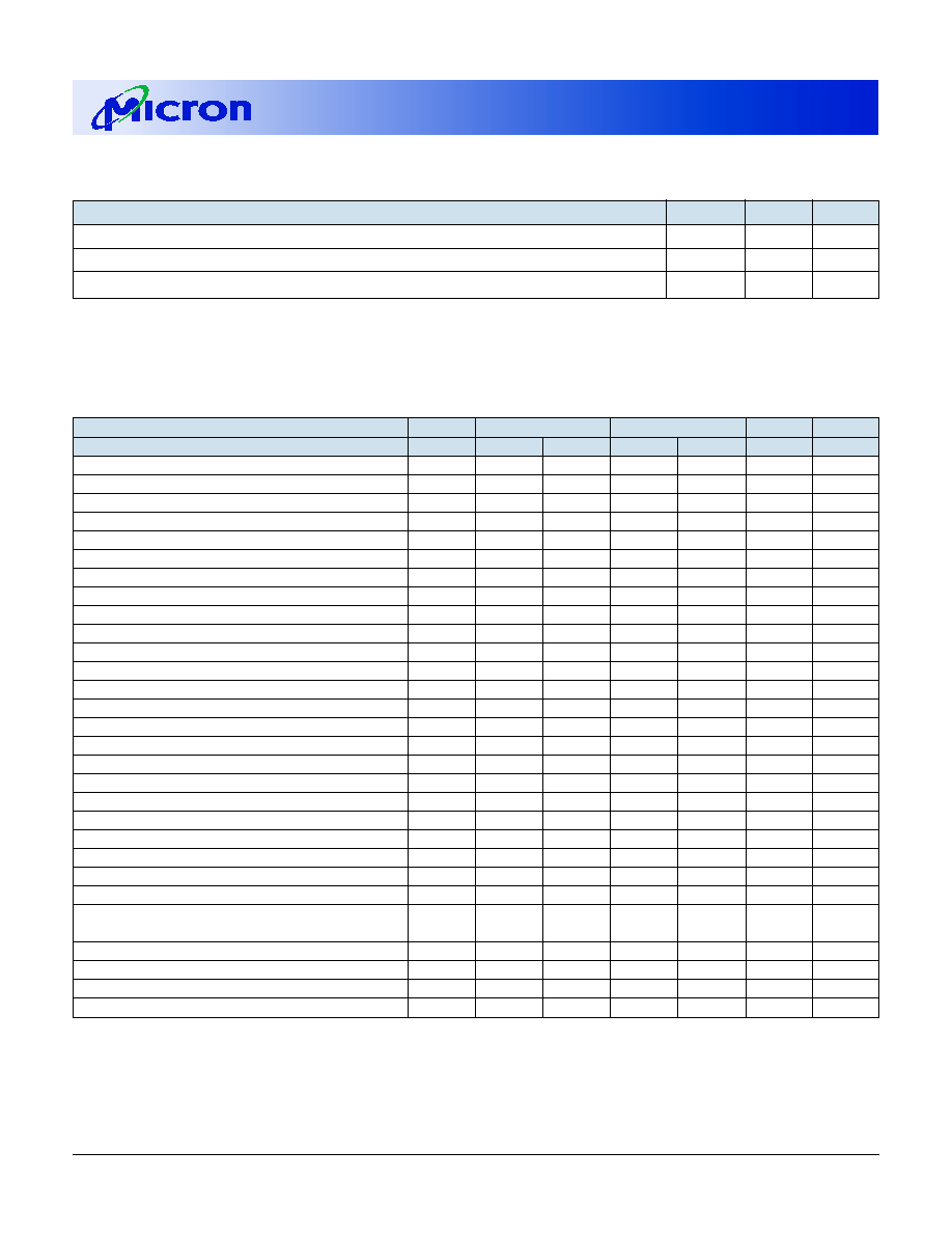
READ CYCLE
tRRH
tCLZ
tCAC
tRAC
tAA
VALID DATA
OPEN
tOFF
tRCH
ROW
tRCS
tASC
tRAH
tRAD
tAR
tCAH
tRCD
tCAS
tRSH
tCSH
tRP
tRC
tRAS
tCRP
tASR
ROW
OPEN
RAS#
V
V
IH
IL
V
V
IH
IL
ADDR
V
V
IH
IL
DQ
V
V
OH
OL
V
V
IH
IL
tOD
tOE
OE#
V
V
IH
IL
COLUMN
CAS#
WE#
NOTE 1
tACH
DON'T CARE
UNDEFINED
NOTE: 1.
t
OFF is referenced from rising edge of RAS# or CAS#, whichever occurs last.
-5
-6
SYMBOL
MIN
MAX
MIN
MAX
UNITS
t
OFF
0
12
0
15
ns
t
RAC
50
60
ns
t
RAD
9
12
ns
t
RAH
9
10
ns
t
RAS
50
10,000
60
10,000
ns
t
RC
84
104
ns
t
RCD
11
14
ns
t
RCH
0
0
ns
t
RCS
0
0
ns
t
RP
30
40
ns
t
RRH
0
0
ns
t
RSH
13
15
ns
TIMING PARAMETERS
-5
-6
SYMBOL
MIN
MAX
MIN
MAX
UNITS
t
AA
25
30
ns
t
ACH
12
15
ns
t
AR
38
45
ns
t
ASC
0
0
ns
t
ASR
0
0
ns
t
CAC
13
15
ns
t
CAH
8
10
ns
t
CAS
8
10,000
10
10,000
ns
t
CLZ
0
0
ns
t
CRP
5
5
ns
t
CSH
38
45
ns
t
OD
0
12
0
15
ns
t
OE
12
15
ns
11
16 Meg x 4 EDO DRAM
Micron Technology, Inc., reserves the right to change products or specifications without notice.
D22_2.p65 ≠ Rev. 5/00
©2000, Micron Technology, Inc.
16 MEG x 4
EDO DRAM
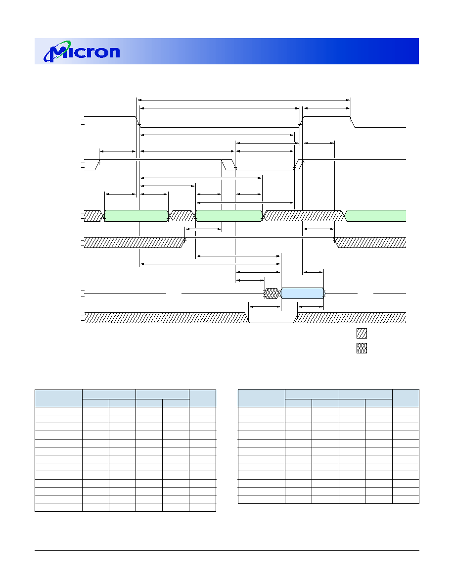
EARLY WRITE CYCLE
DON'T CARE
UNDEFINED
V
V
IH
IL
VALID DATA
ROW
COLUMN
ROW
tDS
tWP
tWCH
tWCS
tWCR
tRWL
tCWL
tCAH
tASC
tRAH
tASR
tRAD
tAR
tCAS
tRSH
tCSH
tRCD
tCRP
tRAS
tRC
tRP
V
V
IH
IL
ADDR
V
V
IH
IL
V
V
IH
IL
DQ
V
V
IOH
IOL
V
V
IH
IL
RAS#
OE#
tDH
WE#
CAS#
tACH
-5
-6
SYMBOL
MIN
MAX
MIN
MAX
UNITS
t
RAH
9
10
ns
t
RAS
50
10,000
60
10,000
ns
t
RC
84
104
ns
t
RCD
11
14
ns
t
RP
30
40
ns
t
RSH
13
15
ns
t
RWL
13
15
ns
t
WCH
8
10
ns
t
WCR
38
45
ns
t
WCS
0
0
ns
t
WP
5
5
ns
TIMING PARAMETERS
-5
-6
SYMBOL
MIN
MAX
MIN
MAX
UNITS
t
ACH
12
15
ns
t
AR
38
45
ns
t
ASC
0
0
ns
t
ASR
0
0
ns
t
CAH
8
10
ns
t
CAS
8
10,000
10
10,000
ns
t
CRP
5
5
ns
t
CSH
38
45
ns
t
CWL
8
15
ns
t
DH
8
10
ns
t
DS
0
0
ns
t
RAD
9
12
ns

12
16 Meg x 4 EDO DRAM
Micron Technology, Inc., reserves the right to change products or specifications without notice.
D22_2.p65 ≠ Rev. 5/00
©2000, Micron Technology, Inc.
16 MEG x 4
EDO DRAM
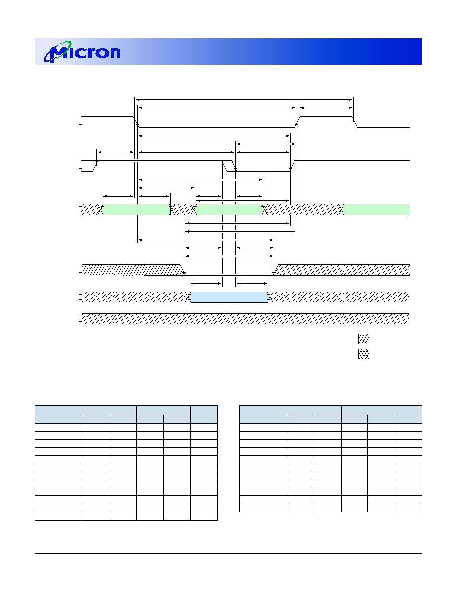
READ-WRITE CYCLE
(LATE WRITE and READ-MODIFY-WRITE cycles)
VALID D
OUT
VALID D
IN
ROW
COLUMN
ROW
V
V
IH
IL
V
V
IH
IL
ADDR
V
V
IH
IL
V
V
IH
IL
DQ
V
V
IOH
IOL
V
V
IH
IL
RAS#
OPEN
OPEN
tOE
tOD
tCAC
tRAC
tAA
tCLZ
tDS
tDH
tAWD
tWP
tRWL
tCWL
tCWD
tRWD
tRCS
tASC
tCAH
tAR
tASR
tRAD
tCRP
tRCD
tCAS
tRSH
tCSH
tRAS
tRWC
tRP
tRAH
OE#
tOEH
WE#
tACH
CAS#
DON' T CARE
UNDEFINED
-5
-6
SYMBOL
MIN
MAX
MIN
MAX
UNITS
t
OD
0
12
0
15
ns
t
OE
12
15
ns
t
OEH
8
10
ns
t
RAC
50
60
ns
t
RAD
9
12
ns
t
RAH
9
10
ns
t
RAS
50
10,000
60
10,000
ns
t
RCD
11
14
ns
t
RCS
0
0
ns
t
RP
30
40
ns
t
RSH
13
15
ns
t
RWC
116
140
ns
t
RWD
67
79
ns
t
RWL
13
15
ns
t
WP
5
5
ns
TIMING PARAMETERS
-5
-6
SYMBOL
MIN
MAX
MIN
MAX
UNITS
t
AA
25
30
ns
t
ACH
12
15
ns
t
AR
38
45
ns
t
ASC
0
0
ns
t
ASR
0
0
ns
t
AWD
42
49
ns
t
CAC
13
15
ns
t
CAH
8
10
ns
t
CAS
8
10,000
10
10,000
ns
t
CLZ
0
0
ns
t
CRP
5
5
ns
t
CSH
38
45
ns
t
CWD
28
35
ns
t
CWL
8
10
ns
t
DH
8
10
ns
t
DS
0
0
ns
13
16 Meg x 4 EDO DRAM
Micron Technology, Inc., reserves the right to change products or specifications without notice.
D22_2.p65 ≠ Rev. 5/00
©2000, Micron Technology, Inc.
16 MEG x 4
EDO DRAM
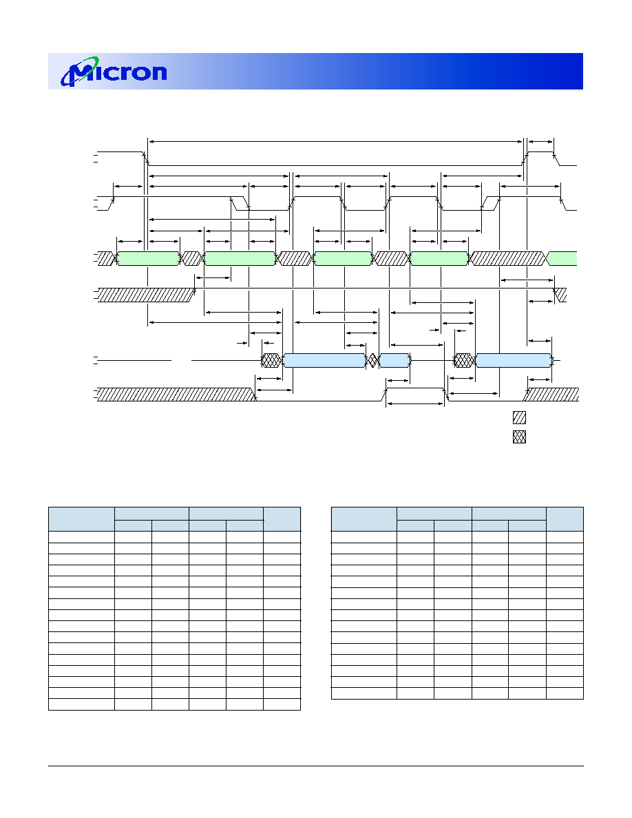
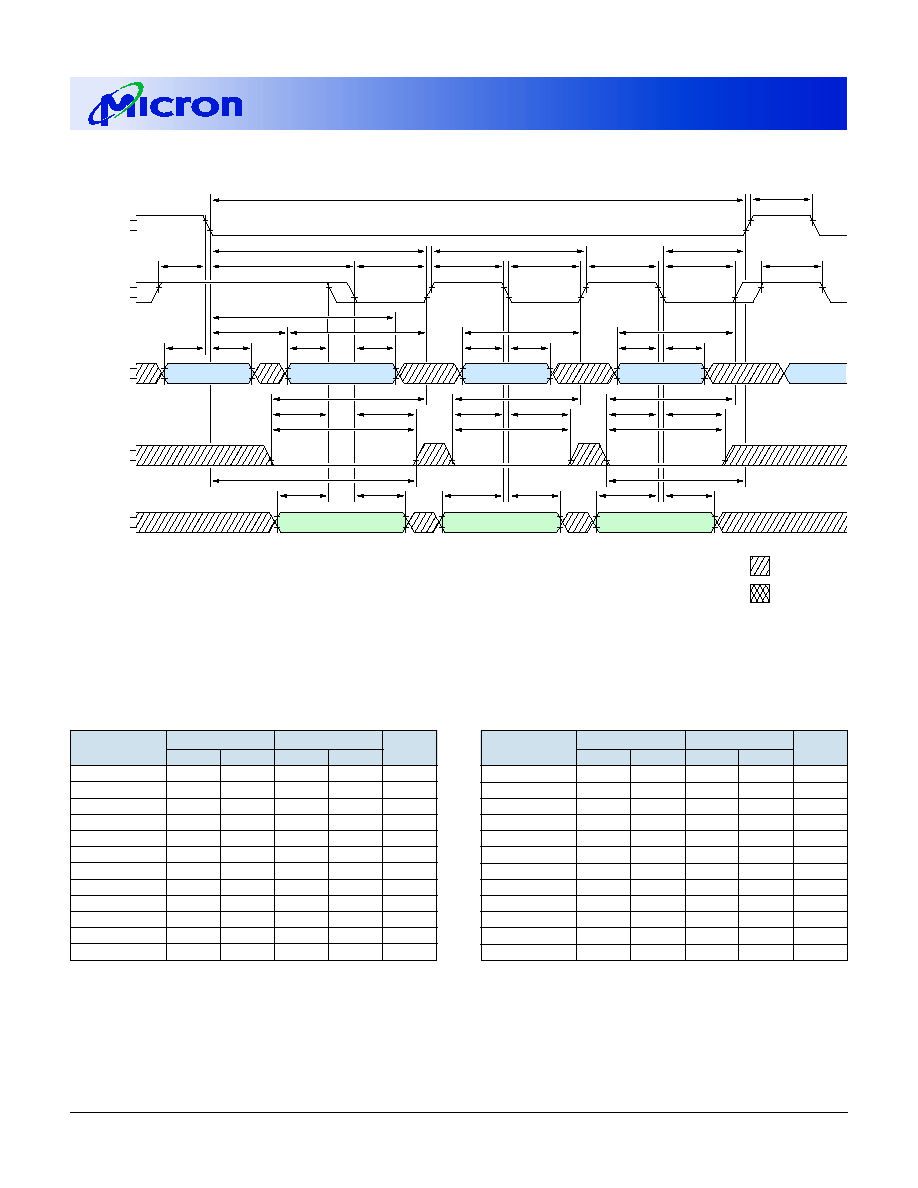
EDO-PAGE-MODE READ CYCLE
VALID
DATA
VALID
DATA
VALID
DATA
COLUMN
COLUMN
COLUMN
ROW
ROW
DON'T CARE
UNDEFINED
tOD
tCAH
tASC
tCP
tRSH
tCP
tCP
tCAS
tRCD
tCRP
tPC
tCSH
tRASP
tRP
tCAH
tASC
tCAH
tASC
tAR
tRAH
tRAD
tASR
tRCS
tRRH
tRCH
tOFF
tCAC
tCPA
tAA
tCLZ
tCAC
tCPA
tAA
tCAC
tRAC
tAA
tCLZ
tOE
tOD
tOE
tOD
OPEN
OPEN
V
V
IH
IL
V
V
IH
IL
ADDR
V
V
IH
IL
V
V
IH
IL
DQ
V
V
OH
OL
V
V
IH
IL
RAS#
OE#
tCAS
tCAS
CAS#
WE#
tCOH
tOEP
tOEHC
tOES
tOES
tACH
tACH
tACH
-5
-6
SYMBOL
MIN
MAX
MIN
MAX
UNITS
t
OEHC
5
10
ns
t
OEP
5
5
ns
t
OES
4
5
ns
t
OFF
0
12
0
15
ns
t
PC
20
25
ns
t
RAC
50
60
ns
t
RAD
9
12
ns
t
RAH
9
10
ns
t
RASP
50
125,000
60
125,000
ns
t
RCH
0
0
ns
t
RCD
11
14
ns
t
RCS
0
0
ns
t
RP
30
40
ns
t
RRH
0
0
ns
t
RSH
13
15
ns
TIMING PARAMETERS
-5
-6
SYMBOL
MIN
MAX
MIN
MAX
UNITS
t
AA
25
30
ns
t
ACH
12
15
ns
t
AR
38
45
ns
t
ASC
0
0
ns
t
ASR
0
0
ns
t
CAC
13
15
ns
t
CAH
8
10
ns
t
CAS
8
10,000
10
10,000
ns
t
CLZ
0
0
ns
t
COH
3
3
ns
t
CP
8
10
ns
t
CPA
28
35
ns
t
CRP
5
5
ns
t
CSH
38
45
ns
t
OD
0
12
0
15
ns
t
OE
12
15
ns
14
16 Meg x 4 EDO DRAM
Micron Technology, Inc., reserves the right to change products or specifications without notice.
D22_2.p65 ≠ Rev. 5/00
©2000, Micron Technology, Inc.
16 MEG x 4
EDO DRAM
tDS
tDH
tDS
tDH
tDS
tDH
tWCR
VALID DATA
VALID DATA
VALID DATA
tRWL
tWP
tCWL
tWCH
tWCS
tWP
tCWL
tWCH
tWCS
tWP
tCWL
tWCH
tWCS
tCAH
tASC
tCAH
tASC
tCAH
tASC
tRAH
tASR
tRAD
tACH
tACH
tACH
tAR
COLUMN
COLUMN
COLUMN
ROW
ROW
tCP
tCAS
tRSH
tCP
tCAS
tCP
tCAS
tRCD
tCRP
tPC
tCSH
tRASP
t RP
V
V
IH
IL
CAS#
V
V
IH
IL
ADDR
V
V
IH
IL
WE#
V
V
IH
IL
DQ
V
V
IOH
IOL
RAS#
DON'T CARE
UNDEFINED
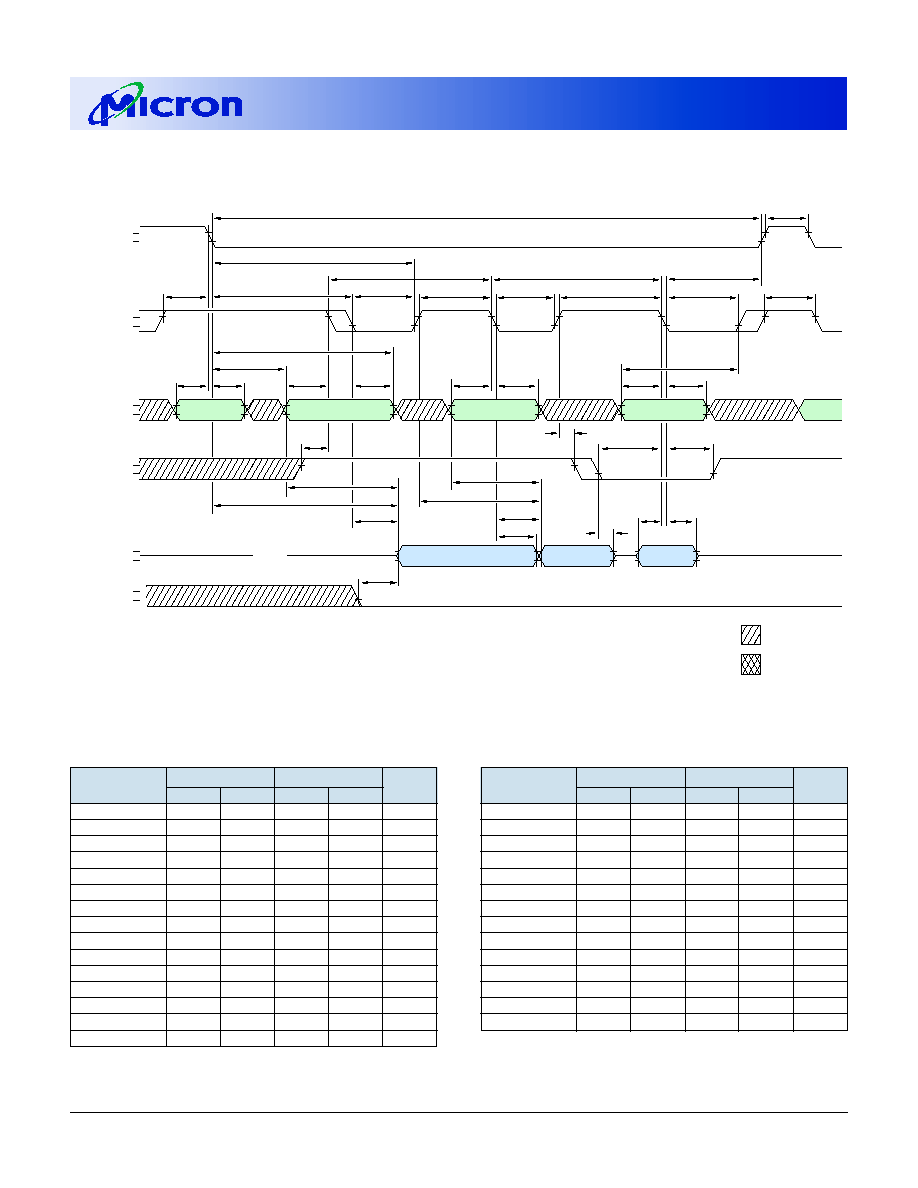
EDO-PAGE-MODE EARLY WRITE CYCLE
-5
-6
SYMBOL
MIN
MAX
MIN
MAX
UNITS
t
PC
20
25
ns
t
RAD
9
12
ns
t
RAH
9
10
ns
t
RASP
50
125,000
60
125,000
ns
t
RCD
11
14
ns
t
RP
30
40
ns
t
RSH
13
15
ns
t
RWL
13
15
ns
t
WCH
8
10
ns
t
WCR
38
45
ns
t
WCS
0
0
ns
t
WP
5
5
ns
TIMING PARAMETERS
-5
-6
SYMBOL
MIN
MAX
MIN
MAX
UNITS
t
ACH
12
15
ns
t
AR
38
45
ns
t
ASC
0
0
ns
t
ASR
0
0
ns
t
CAH
8
10
ns
t
CAS
8
10,000
10
10,000
ns
t
CP
8
10
ns
t
CRP
5
5
ns
t
CSH
38
45
ns
t
CWL
8
10
ns
t
DH
8
10
ns
t
DS
0
0
ns

15
16 Meg x 4 EDO DRAM
Micron Technology, Inc., reserves the right to change products or specifications without notice.
D22_2.p65 ≠ Rev. 5/00
©2000, Micron Technology, Inc.
16 MEG x 4
EDO DRAM
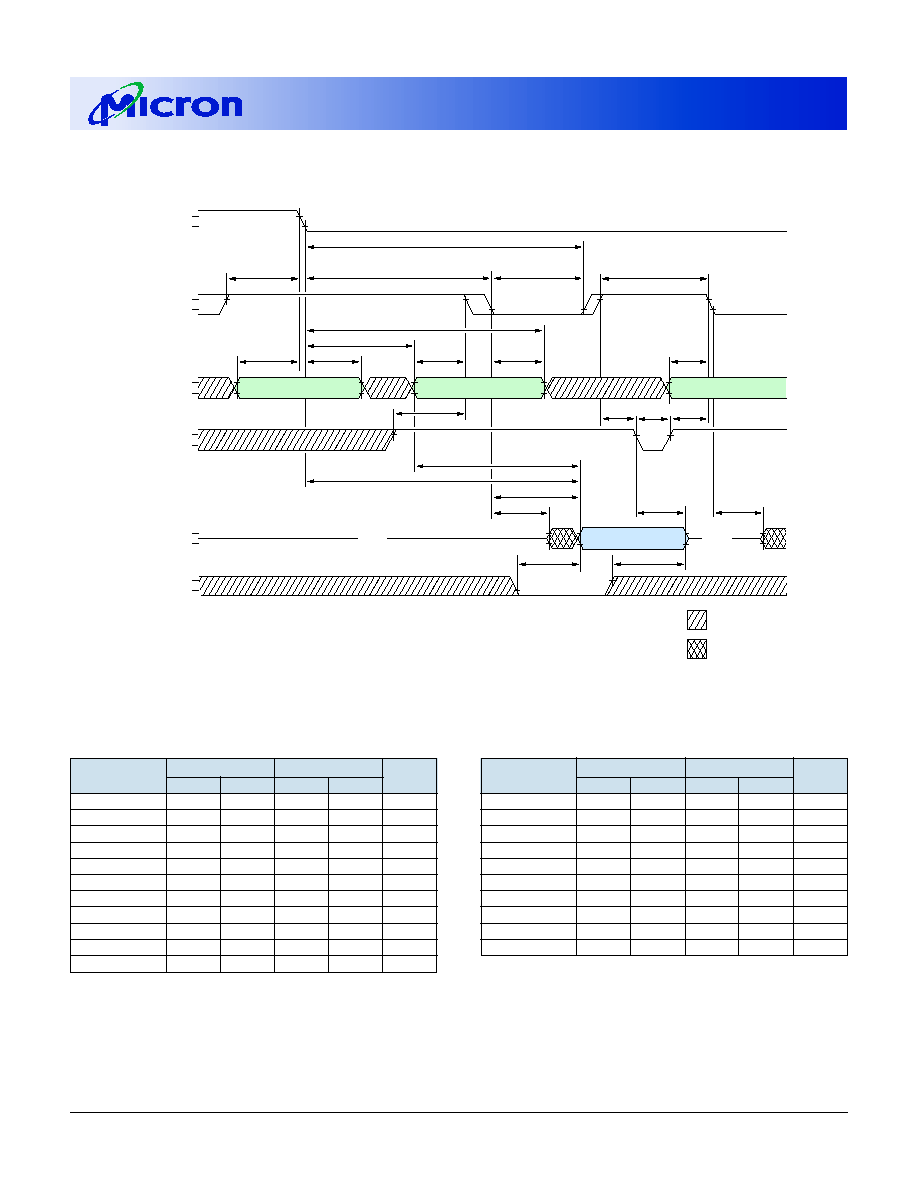
EDO-PAGE-MODE READ-WRITE CYCLE
(LATE WRITE and READ-MODIFY-WRITE cycles)
VALID D
OUT
VALID D
IN
ROW
COLUMN
ROW
V
V
IH
IL
V
V
IH
IL
ADDR
V
V
IH
IL
V
V
IH
IL
DQ
V
V
IOH
IOL
V
V
IH
IL
RAS#
OPEN
OPEN
tOE
tOD
tCAC
tRAC
tAA
tCLZ
tDS
tDH
tAWD
tWP
tRWL
tCWL
tCWD
tRWD
tRCS
tASC
tCAH
tAR
tASR
tRAD
tCRP
tRCD
tCAS
tRSH
tCSH
tRAS
tRWC
tRP
tRAH
OE#
tOEH
WE#
tACH
CAS#
DON'T CARE
UNDEFINED
NOTE: 1.
t
PC is for LATE WRITE cycles only.
-5
-6
SYMBOL
MIN
MAX
MIN
MAX
UNITS
t
OD
0
12
0
15
ns
t
OE
12
15
ns
t
OEH
8
10
ns
t
PC
20
25
ns
t
PRWC
47
56
ns
t
RAC
50
60
ns
t
RAD
9
12
ns
t
RAH
9
10
ns
t
RASP
50
125,000
60
125,000
ns
t
RCD
11
14
ns
t
RCS
0
0
ns
t
RP
30
40
ns
t
RSH
13
15
ns
t
RWD
67
79
ns
t
RWL
13
15
ns
t
WP
5
5
ns
TIMING PARAMETERS
-5
-6
SYMBOL
MIN
MAX
MIN
MAX
UNITS
t
AA
25
30
ns
t
AR
38
45
ns
t
ASC
0
0
ns
t
ASR
0
0
ns
t
AWD
42
49
ns
t
CAC
13
15
ns
t
CAH
8
10
ns
t
CAS
8
10,000
10
10,000
ns
t
CLZ
0
0
ns
t
CP
8
10
ns
t
CPA
28
35
ns
t
CRP
5
5
ns
t
CSH
38
45
ns
t
CWD
28
35
ns
t
CWL
8
10
ns
t
DH
8
10
ns
t
DS
0
0
ns
16
16 Meg x 4 EDO DRAM
Micron Technology, Inc., reserves the right to change products or specifications without notice.
D22_2.p65 ≠ Rev. 5/00
©2000, Micron Technology, Inc.
16 MEG x 4
EDO DRAM
EDO-PAGE-MODE READ EARLY WRITE CYCLE
(Pseudo READ-MODIFY-WRITE)
V
V
IH
IL
V
V
IH
IL
RAS#
V
V
IH
IL
ADDR
V
V
IH
IL
WE#
tRASP
tRP
ROW
COLUMN (A)
COLUMN (N)
ROW
V
V
IH
IL
OE#
V
V
IOH
IOL
tCRP
tCSH
tCAS
tRCD
tASR
tRAH
tRAD
tASC
tAR
tCAH
tASC
tCAH
tASC
tCAH
tCP
tRSH
VALID DATA
IN
tRCS
tRCH
tWCS
tOE
VALID
DATA (B)
VALID DATA (A)
tWHZ
tCAC
tCPA
tAA
tCAC
tAA
OPEN
DQ
tPC
RAC
t
tCOH
tWCH
tDS
tDH
tPC
COLUMN (B)
tACH
CAS#
tCAS
tCAS
tCP
tCP
DON'T CARE
UNDEFINED
-5
-6
SYMBOL
MIN
MAX
MIN
MAX
UNITS
t
OE
12
15
ns
t
PC
20
25
ns
t
RAC
50
60
ns
t
RAD
9
12
ns
t
RAH
9
10
ns
t
RASP
50
125,000
60
125,000
ns
t
RCD
11
14
ns
t
RCH
0
0
ns
t
RCS
0
0
ns
t
RP
30
40
ns
t
RSH
13
15
ns
t
WCH
8
10
ns
t
WCS
0
0
ns
t
WHZ
0
12
0
15
ns
TIMING PARAMETERS
-5
-6
SYMBOL
MIN
MAX
MIN
MAX
UNITS
t
AA
25
30
ns
t
ACH
12
15
ns
t
AR
38
45
ns
t
ASC
0
0
ns
t
ASR
0
0
ns
t
CAC
13
15
ns
t
CAH
8
10
ns
t
CAS
8
10,000
10
10,000
ns
t
COH
3
3
ns
t
CP
8
10
ns
t
CPA
28
35
ns
t
CRP
5
5
ns
t
CSH
38
45
ns
t
DH
8
10
ns
t
DS
0
0
ns
17
16 Meg x 4 EDO DRAM
Micron Technology, Inc., reserves the right to change products or specifications without notice.
D22_2.p65 ≠ Rev. 5/00
©2000, Micron Technology, Inc.
16 MEG x 4
EDO DRAM
READ CYCLE
(With WE#-controlled disable)
tCLZ
tCAC
tRAC
tAA
VALID DATA
OPEN
tRCH
tRCS
tASC
tRAH
tRAD
tAR
tCAH
tRCD
tCAS
tCSH
tCRP
tASR
ROW
OPEN
RAS#
V
V
IH
IL
V
V
IH
IL
ADDR
V
V
IH
IL
DQ
V
V
OH
OL
V
V
IH
IL
tOD
tOE
OE#
V
V
IH
IL
COLUMN
WE#
tWHZ
tWPZ
tCP
tASC
tRCS
COLUMN
tCLZ
DON'T CARE
UNDEFINED
CAS#
-5
-6
SYMBOL
MIN
MAX
MIN
MAX
UNITS
t
OD
0
12
0
15
ns
t
OE
12
15
ns
t
RAC
50
60
ns
t
RAD
9
12
ns
t
RAH
9
10
ns
t
RCD
11
14
ns
t
RCH
0
0
ns
t
RCS
0
0
ns
t
WHZ
0
12
0
15
ns
t
WPZ
10
10
ns
TIMING PARAMETERS
-5
-6
SYMBOL
MIN
MAX
MIN
MAX
UNITS
t
AA
25
30
ns
t
AR
38
45
ns
t
ASC
0
0
ns
t
ASR
0
0
ns
t
CAC
13
15
ns
t
CAH
8
10
ns
t
CAS
8
10,000
10
10,000
ns
t
CLZ
0
0
ns
t
CP
8
10
ns
t
CRP
5
5
ns
t
CSH
38
45
ns

18
16 Meg x 4 EDO DRAM
Micron Technology, Inc., reserves the right to change products or specifications without notice.
D22_2.p65 ≠ Rev. 5/00
©2000, Micron Technology, Inc.
16 MEG x 4
EDO DRAM
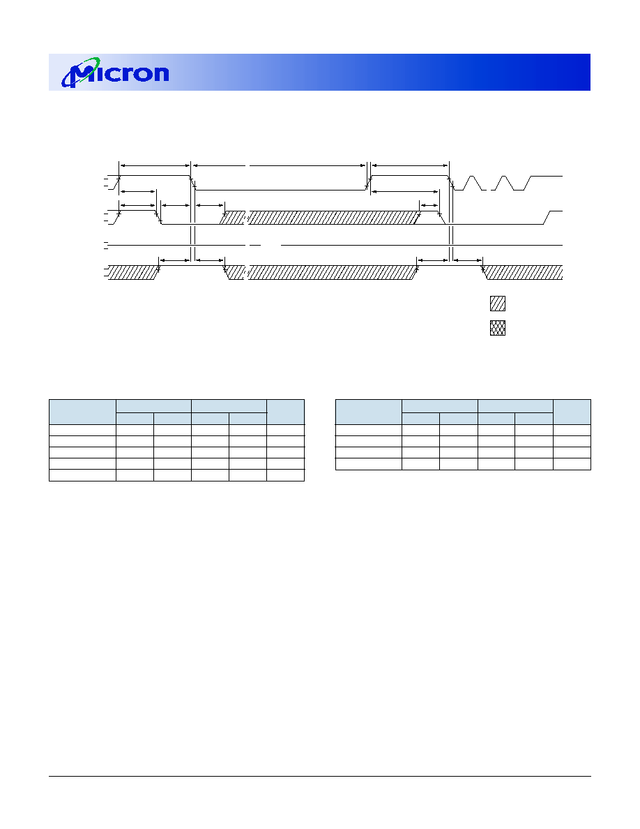
RAS#-ONLY REFRESH CYCLE
(OE# and WE# = DON'T CARE)
ROW
V
V
IH
IL
CAS#
V
V
IH
IL
ADDR
V
V
IH
IL
RAS#
tRC
tRAS
tRP
tCRP
tASR
tRAH
ROW
OPEN
DQ
V
V
OH
OL
tRPC
CBR REFRESH CYCLE
(Addresses and OE# = DON'T CARE)
tRP
V
V
IH
IL
RAS#
tRAS
NOTE 1
OPEN
tCHR
tCSR
V
V
IH
IL
V
V
OH
OL
CAS#
DQ
tRP
tRAS
tRPC
tCSR
tRPC
tCHR
tCP
V
V
IH
IL
tWRP
tWRH
WE#
tWRP
tWRH
DON'T CARE
UNDEFINED
-5
-6
SYMBOL
MIN
MAX
MIN
MAX
UNITS
t
RAS
50
10,000
60
10,000
ns
t
RC
84
104
ns
t
RP
30
40
ns
t
RPC
5
5
ns
t
WRH
8
10
ns
t
WRP
8
10
ns
TIMING PARAMETERS
-5
-6
SYMBOL
MIN
MAX
MIN
MAX
UNITS
t
ASR
0
0
ns
t
CHR
8
10
ns
t
CP
8
10
ns
t
CRP
5
5
ns
t
CSR
5
5
ns
t
RAH
9
10
ns
NOTE: 1. End of first CBR REFRESH cycle.

19
16 Meg x 4 EDO DRAM
Micron Technology, Inc., reserves the right to change products or specifications without notice.
D22_2.p65 ≠ Rev. 5/00
©2000, Micron Technology, Inc.
16 MEG x 4
EDO DRAM
HIDDEN REFRESH CYCLE
1
(WE# = HIGH; OE# = LOW)
DON'T CARE
UNDEFINED
tCLZ
tOFF
OPEN
VALID DATA
OPEN
COLUMN
ROW
tCAC
tRAC
tAA
tCAH
tASC
tRAH
tASR
tRAD
tAR
tCRP
tRCD
tRSH
tRAS
tRP
tCHR
tRAS
DQ
V
V
OH
OL
V
V
IH
IL
ADDR
V
V
IH
IL
V
V
IH
IL
RAS#
V
V
IH
IL
tOE
tOD
OE#
tORD
CAS#
-5
-6
SYMBOL
MIN
MAX
MIN
MAX
UNITS
t
OE
12
15
ns
t
OFF
0
12
0
15
ns
t
ORD
0
0
ns
t
RAC
50
60
ns
t
RAD
9
12
ns
t
RAH
9
10
ns
t
RAS
50
10,000
60
10,000
ns
t
RCD
11
14
ns
t
RP
30
40
ns
t
RSH
13
15
ns
TIMING PARAMETERS
-5
-6
SYMBOL
MIN
MAX
MIN
MAX
UNITS
t
AA
25
30
ns
t
AR
38
45
ns
t
ASC
0
0
ns
t
ASR
0
0
ns
t
CAC
13
15
ns
t
CAH
8
10
ns
t
CHR
8
10
ns
t
CLZ
0
0
ns
t
CRP
5
5
ns
t
OD
0
12
0
15
ns
NOTE: 1. A HIDDEN REFRESH may also be performed after a WRITE cycle. In this case, WE# is LOW and OE# is HIGH.
20
16 Meg x 4 EDO DRAM
Micron Technology, Inc., reserves the right to change products or specifications without notice.
D22_2.p65 ≠ Rev. 5/00
©2000, Micron Technology, Inc.
16 MEG x 4
EDO DRAM
SELF REFRESH CYCLE
(Addresses and OE# = DON'T CARE)
V
V
IH
IL
RAS#
tRASS
OPEN
V
V
IH
IL
V
V
OH
OL
DQ
tRPC
tCHD
tRPS
tRPC
tRP
tCP
CAS#
WE#
V
V
IH
IL
tWRH
tWRP
tWRH
tWRP
(
)
(
)
(
)
(
)
(
)
(
)
(
)
(
)
(
)
(
)
(
)
(
)
NOTE 1
tCSR
DON'T CARE
UNDEFINED
tCP
NOTE 2
(
)
(
)
(
)
(
)
NOTE: 1. Once
t
RASS (MIN) is met and RAS# remains LOW, the DRAM will enter self refresh mode.
2. Once
t
RPS is satisfied, a complete burst of all rows should be executed if RAS#-only por Burst CBR refresh is being used.
-5
-6
SYMBOL
MIN
MAX
MIN
MAX
UNITS
t
RPC
5
5
ns
t
RPS
90
105
ns
t
WRH
8
10
ns
t
WRP
8
10
ns
TIMING PARAMETERS
-5
-6
SYMBOL
MIN
MAX
MIN
MAX
UNITS
t
CHD
15
15
ns
t
CP
8
10
ns
t
CSR
5
5
ns
t
RASS
100
100
µs
t
RP
30
40
ns
21
16 Meg x 4 EDO DRAM
Micron Technology, Inc., reserves the right to change products or specifications without notice.
D22_2.p65 ≠ Rev. 5/00
©2000, Micron Technology, Inc.
16 MEG x 4
EDO DRAM
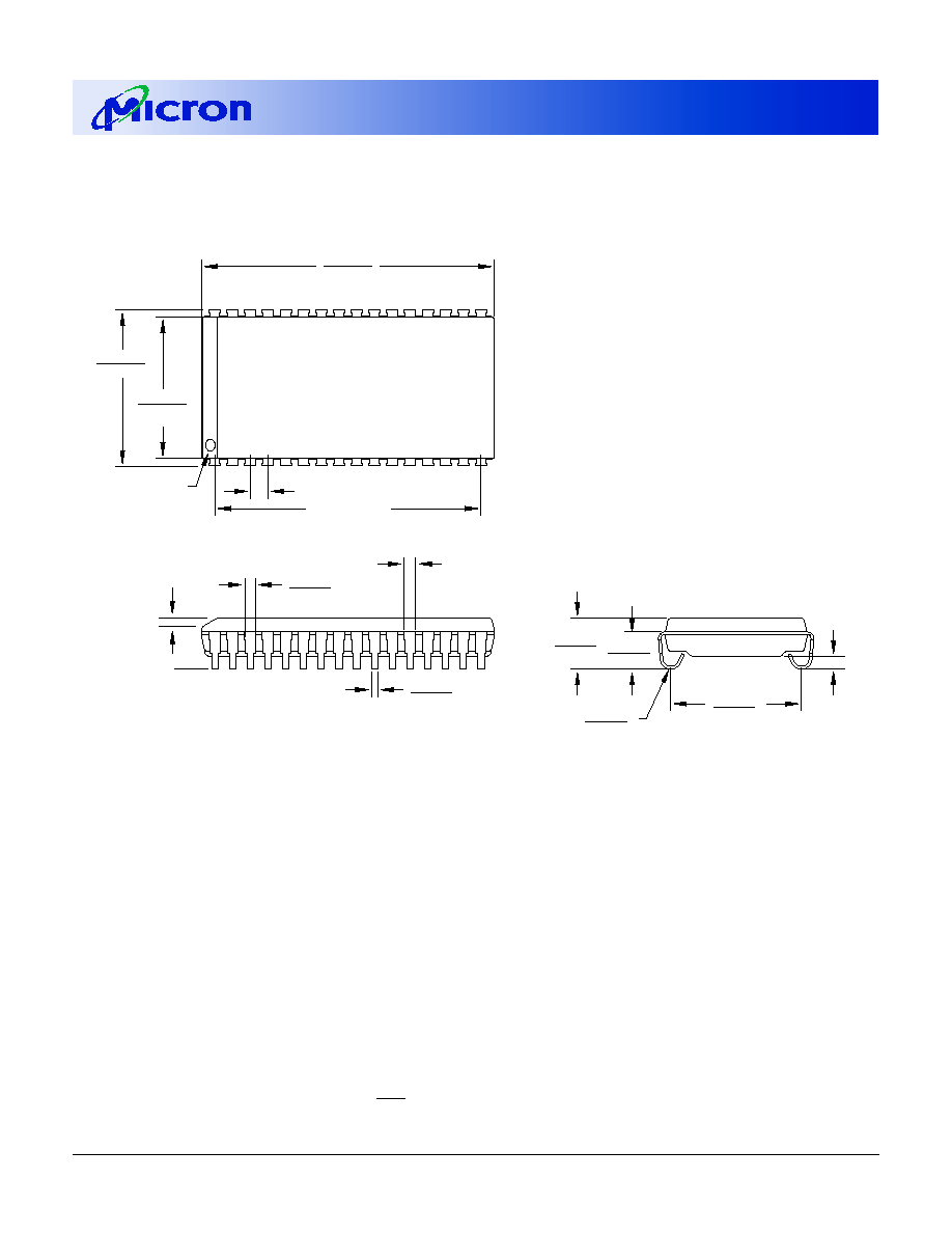
32-PIN PLASTIC SOJ (400 mil)
.435 (11.05)
.360 (9.14)
.750 (19.05) TYP
.829 (21.05)
SEATING PLANE
.040 (1.02)
.380 (9.65)
.080 (2.03)
.095 (2.42)
.145 (3.68)
.132 (3.35)
.015 (0.38)
.020 (0.51)
PIN #1 ID
.050 (1.27) TYP
.445 (11.31)
.823 (20.90)
.405 (10.29)
.399 (10.13)
.030 (0.77)
R
.032 (0.82)
.037 (0.95) MAX DAMBAR PROTRUSION
.026 (0.67)
.024 (0.61)
.030 (0.76)
MIN
NOTE: 1. All dimensions in inches (millimeters) MAX or typical where noted.
MIN
2. Package width and length do not include mold protrusion; allowable mold protrusion is .01" per side.

22
16 Meg x 4 EDO DRAM
Micron Technology, Inc., reserves the right to change products or specifications without notice.
D22_2.p65 ≠ Rev. 5/00
©2000, Micron Technology, Inc.
16 MEG x 4
EDO DRAM
32-PIN PLASTIC TSOP (400 mil)
.008 (0.20)
.002 (0.05)
.467 (11.86)
.459 (11.66)
.047(1.19)
MAX
.024 (0.60)
.016 (0.40)
32
1
16
GAGE PLANE
.010 (0.25)
SEE DETAIL A
.004 (0.10)
.007 (0.18)
.005 (0.13)
.827 (21.01)
.823 (20.91)
DETAIL A
.0375 (0.95)
.402 (10.21)
.398 (10.11)
.020 (0.50)
.012 (0.30)
.0315 (0.80)
.050 (1.27)
TYP
NOTE: 1. All dimensions in inches (millimeters) MAX or typical where noted.
MIN
2. Package width and length do not include mold protrusion; allowable mold protrusion is .01" per side.
8000 S. Federal Way, P.O. Box 6, Boise, ID 83707-0006, Tel: 208-368-3900
E-mail: prodmktg@micron.com, Internet: http://www.micron.com, Customer Comment Line: 800-932-4992
Micron is a registered trademark of Micron Technology, Inc.