Document Outline
- Features/Options
- General Description
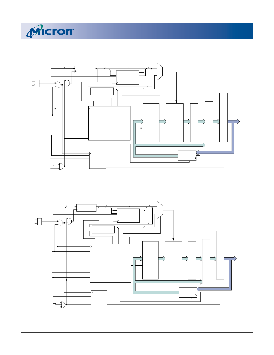
- Functional Block Diagram 128K x 18
- Functional Block Diagram 64K x 32/36
- General Description (continued)
- Pin Assignment Table
- Pin Assignment (Top View) 100-Pin TQFP
- Pin Descriptions
- Pin Descriptions (continued)
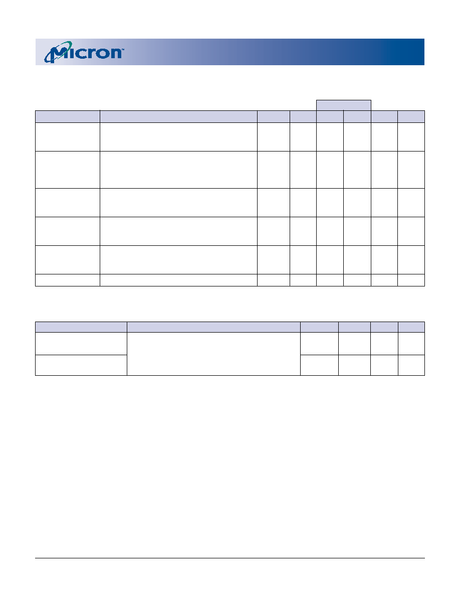
- Interleaved Burst Address Table (Mode = NC or HIGH)
- Linear Burst Address Table (Mode = NC or LOW)
- Partial Truth Table for READ/WRITE Commands (x18)
- Partial Truth Table for READ/WRITE Commands (x32/36)
- State Diagram for ZBT SRAM
- Truth Table
- Absolute Maximum Ratings
- DC Electrical Characteristics and Operating Conditions
- TQFP Capacitance
- IDD Operating Conditions and Maximum Limits
- TQFP Thermal Resistance
- Electrical Characteristics
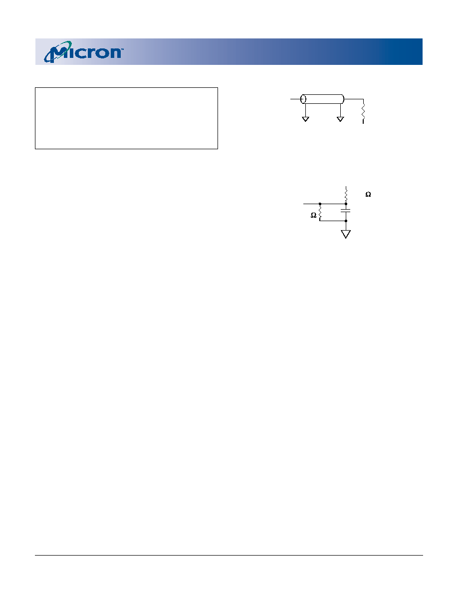
- AC Test Conditions
- Load Derating Curves
- Output Load Equivalents
- SNOOZE MODE
- SNOOZE MODE Electrical Characteristics
- SNOOZE MODE Waveform
- READ/WRITE Timing
- NOP, STALL and DESELECT Cycles
- 100-Pin Plastic TQFP (JEDEC LQFP)
- Revision History
1
2Mb: 128K x 18, 64K x 32/36 3.3V I/O, Flow-Through ZBT SRAM
©2002, Micron Technology, Inc.
MT55L128L18F1_C.p65 ≠ Rev. C, Pub. 11/02
2Mb: 128K x 18, 64K x 32/36
3.3V I/O, FLOW-THROUGH ZBT SRAM
NOT RECOMENDED FOR NEW DESIGNS
PRODUCTS AND SPECIFICATIONS DISCUSSED HEREIN ARE SUBJECT TO CHANGE BY MICRON WITHOUT NOTICE.
2Mb
ZBT
Æ
SRAM
FEATURES
∑ High frequency and 100 percent bus utilization
∑ Fast cycle times: 10ns and 12ns
∑ Single +3.3V ±5% power supply
∑ Advanced control logic for minimum control signal
interface
∑ Individual BYTE WRITE controls may be tied LOW
∑ Single R/W# (read/write) control pin
∑ CKE# pin to enable clock and suspend operations
∑ Three chip enables for simple depth expansion
∑ Clock-controlled and registered addresses, data
I/Os and control signals
∑ Internally self-timed, fully coherent WRITE
∑ Internally self-timed, registered outputs eliminate
the need to control OE#
∑ SNOOZE MODE for reduced-power standby
∑ Common data inputs and data outputs
∑ Linear or Interleaved Burst Modes
∑ Burst feature (optional)
∑ 100-pin TQFP package
∑ Pin/function compatibility with 4Mb, 8Mb, and
16Mb ZBT SRAM
∑ Automatic power-down
OPTIONS
MARKING*
∑ Timing (Access/Cycle/MHz)
7.5ns/10ns/100 MHz
-10
9ns/12ns/83 MHz
-12
∑ Configurations
128K x 18
MT55L128L18F1
64K x 32
MT55L64L32F1
64K x 36
MT55L64L36F1
∑ Package
100-pin TQFP
T
∑ Temperature
Commercial (0∞C to +70∞C)
None
Part Number Example:
MT55L128L18F1T-10
MT55L128L18F1,
MT55L64L32F1, MT55L64L36F1
3.3V V
DD
, 3.3V I/O
GENERAL DESCRIPTION
The Micron
Æ
Zero Bus Turnaround
TM
(ZBT
Æ
) SRAM
family employs high-speed, low-power CMOS designs
using an advanced CMOS process.
The MT55L128L18F1 and MT55L64L32/36F1
SRAMs integrate a 128K x 18, 64K x 32, or 64K x 36 SRAM
core with advanced synchronous peripheral circuitry
and a 2-bit burst counter. These SRAMs are optimized
for 100 percent bus utilization, eliminating turnaround
cycles for READ to WRITE, or WRITE to READ, transi-
tions. All synchronous inputs pass through registers
controlled by a positive-edge-triggered single clock in-
put (CLK). The synchronous inputs include all ad-
dresses, all data inputs, chip enable (CE#), two addi-
tional chip enables for easy depth expansion (CE2,
CE2#), cycle start input (ADV/LD#), synchronous clock
enable (CKE#), byte write enables (BWa#, BWb#, BWc#
and BWd#) and read/write (R/W#).
Asynchronous inputs include the output enable
(OE#, which may be tied LOW for control signal minimi-
zation), clock (CLK) and snooze enable (ZZ, which may
be tied LOW if unused). There is also a burst mode pin
(MODE) that selects between interleaved and linear
burst modes. MODE may be tied HIGH, LOW or left
unconnected if burst is unused. The flow-through data-
out (Q) is enabled by OE#. WRITE cycles can be from
one to four bytes wide as controlled by the write control
inputs.
**JEDEC-standard MS-026 BHA (LQFP).
100-Pin TQFP**
2
2Mb: 128K x 18, 64K x 32/36 3.3V I/O, Flow-Through ZBT SRAM
Micron Technology, Inc., reserves the right to change products or specifications without notice.
MT55L128L18F1_C.p65 ≠ Rev. C, Pub. 11/02
©2002, Micron Technology, Inc.
2Mb: 128K x 18, 64K x 32/36
3.3V I/O, FLOW-THROUGH ZBT SRAM
NOT RECOMENDED FOR NEW DESIGNS
K
MODE
16
BWa#
BWb#
R/W#
CE#
CE2
CE2#
OE#
READ LOGIC
DQs
DQPa
DQPb
DQPc
DQPd
BWc#
BWd#
ADDRESS
REGISTER
WRITE REGISTRY
AND DATA COHERENCY
CONTROL LOGIC
16
16
14
16
BURST
LOGIC
SA0'
SA1'
D1
D0
Q1
Q0
SA0
SA1
16
ADV/LD#
CE
ADV/LD#
K
CLK
CKE#
WRITE ADDRESS
REGISTER
SA0, SA1, SA
36
36
36
36
64K x 8 x 4
(x32)
64K x 9 x 4
(x36)
MEMORY
ARRAY
D
A
T
A
S
T
E
E
R
I
N
G
O
U
T
P
U
T
B
U
F
F
E
R
S
S
E
N
S
E
A
M
P
S
WRITE
DRIVERS
E
INPUT
REGISTER
E
NOTE: Functional Block Diagrams illustrate simplified device operation. See Truth Table, Pin Descriptions and timing diagrams
for detailed information.
FUNCTIONAL BLOCK DIAGRAM
64K x 32/36
FUNCTIONAL BLOCK DIAGRAM
128K x 18
SA0, SA1, SA
K
MODE
17
BWa#
BWb#
R/W#
CE#
CE2
CE2#
OE#
READ LOGIC
DQs
DQPa
DQPb
O
U
T
P
U
T
B
U
F
F
E
R
S
128K x 9 x 2
MEMORY
ARRAY
E
ADDRESS
REGISTER
WRITE REGISTRY
AND DATA COHERENCY
CONTROL LOGIC
17
17
15
17
BURST
LOGIC
SA0'
SA1'
D1
D0
Q1
Q0
SA0
SA1
17
ADV/LD#
CE
ADV/LD#
K
S
E
N
S
E
A
M
P
S
CLK
CKE#
WRITE ADDRESS
REGISTER
E
INPUT
REGISTER
WRITE
DRIVERS
D
A
T
A
S
T
E
E
R
I
N
G
18
18
18
18

3
2Mb: 128K x 18, 64K x 32/36 3.3V I/O, Flow-Through ZBT SRAM
Micron Technology, Inc., reserves the right to change products or specifications without notice.
MT55L128L18F1_C.p65 ≠ Rev. C, Pub. 11/02
©2002, Micron Technology, Inc.
2Mb: 128K x 18, 64K x 32/36
3.3V I/O, FLOW-THROUGH ZBT SRAM
NOT RECOMENDED FOR NEW DESIGNS
GENERAL DESCRIPTION (continued)
PIN ASSIGNMENT TABLE
PIN #
x18
x32
x36
1
NC
NC
DQPc
2
NC
DQc
DQc
3
NC
DQc
DQc
4
V
DD
Q
5
V
S S
6
NC
DQc
DQc
7
NC
DQc
DQc
8
DQb
DQc
DQc
9
DQb
DQc
DQc
10
V
S S
11
V
DD
Q
12
DQb
DQc
DQc
13
DQb
DQc
DQc
14
V
S S
15
V
DD
16
V
DD
17
V
SS
18
DQb
DQd
DQd
19
DQb
DQd
DQd
20
V
DD
Q
21
V
SS
22
DQb
DQd
DQd
23
DQb
DQd
DQd
24
DQPb
DQd
DQd
25
NC
DQd
DQd
PIN #
x18
x32
x36
51
NC
NC
DQPa
52
NC
DQa
DQa
53
NC
DQa
DQa
54
V
DD
Q
55
V
SS
56
NC
DQa
DQa
57
NC
DQa
DQa
58
DQa
59
DQa
60
V
SS
61
V
DD
Q
62
DQa
63
DQa
64
ZZ
65
V
DD
66
V
SS
67
V
SS
68
DQa
DQb
DQb
69
DQa
DQb
DQb
70
V
DD
Q
71
V
SS
72
DQa
DQb
DQb
73
DQa
DQb
DQb
74
DQPa
DQb
DQb
75
NC
DQb
DQb
PIN #
x18
x32
x36
76
V
S S
77
V
DD
Q
78
NC
DQb
DQb
79
NC
DQb
DQb
80
SA
NC
DQPb
81
SA
82
SA
83
NF*
84
NF*
85
ADV/LD#
86
OE# (G#)
87
CKE#
88
R/W#
89
CLK
90
V
SS
91
V
DD
92
CE2#
93
BWa#
94
BWb#
95
NC
BWc# BWc#
96
NC
BWd# BWd#
97
CE2
98
CE#
99
SA
100
SA
26
V
S S
27
V
DD
Q
28
NC
DQd
DQd
29
NC
D
Qd
DQd
30
NC
NC
DQPd
31
MODE (LBO#)
32
SA
33
SA
34
SA
35
SA
36
SA1
37
SA0
38
DNU
39
DNU
40
V
SS
41
V
DD
42
DNU
43
DNU
44
SA
45
SA
46
SA
47
SA
48
SA
49
SA
50
NC/
SA
*
PIN #
x18
x32
x36
* Pins 50, 83, and 84 are reserved for address expansion.
All READ, WRITE and DESELECT cycles are initi-
ated by the ADV/LD# input. Subsequent burst ad-
dresses can be internally generated as controlled by
the burst advance pin (ADV/LD#). Use of burst mode
is optional. It is allowable to give an address for each
individual READ and WRITE cycle. BURST cycles wrap
around after the fourth access from a base address.
To allow for continuous, 100 percent use of the data
bus, the flow-through ZBT SRAM uses a LATE WRITE
cycle. For example, if a WRITE cycle begins in clock
cycle one, the address is present on rising edge one.
BYTE WRITEs need to be asserted on the same cycle as
the address. The write data associated with the ad-
dress is required one cycle later, or on the rising edge of
clock cycle two.
Address and write control are registered on-chip to
simplify WRITE cycles. This allows self-timed WRITE
cycles. Individual byte enables allow individual bytes
to be written. During a BYTE WRITE cycle, BWa# con-
trols DQa pins; BWb# controls DQb pins; BWc# controls
DQc pins; and BWd# controls DQd pins. Cycle types
can only be defined when an address is loaded, i.e.,
when ADV/LD# is LOW. Parity/ECC bits are only avail-
able on the x18 and x36 versions.
Micron's 2Mb ZBT
SRAMs operate from a +3.3V V
DD
power supply, and all inputs and outputs are LVTTL-
compatible. The device is ideally suited for systems
requiring high bandwidth and zero bus turnaround
delays.
Please refer to Micron's Web site (
www.micron.com/
sramds
) for the latest data sheet.
4
2Mb: 128K x 18, 64K x 32/36 3.3V I/O, Flow-Through ZBT SRAM
Micron Technology, Inc., reserves the right to change products or specifications without notice.
MT55L128L18F1_C.p65 ≠ Rev. C, Pub. 11/02
©2002, Micron Technology, Inc.
2Mb: 128K x 18, 64K x 32/36
3.3V I/O, FLOW-THROUGH ZBT SRAM
NOT RECOMENDED FOR NEW DESIGNS
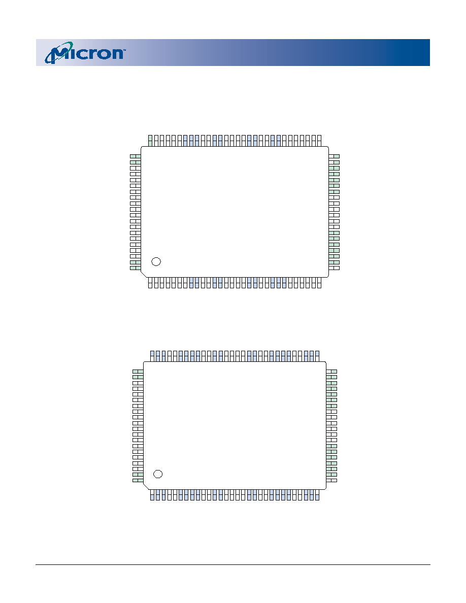
PIN ASSIGNMENT (Top View)
100-Pin TQFP
* NC for x32 version, DQPx for x36 version.
** Pins 50, 83 and 84 are reserved for address expansion.
SA
SA
NF**
NF**
ADV/LD#
OE# (G#)
CKE#
R/W#
CLK
V
SS
V
DD
CE2#
BWa#
BWb#
NC
NC
CE2
CE#
SA
SA
81
82
83
84
85
86
87
88
89
90
91
92
93
94
95
96
97
98
99
100
50
49
48
47
46
45
44
43
42
41
40
39
38
37
36
35
34
33
32
31
80 79 78 77 76 75 74 73 72 71 70 69 68 67 66 65 64 63 62 61 60 59 58 57 56 55 54 53 52 51
1 2 3 4 5 6 7 8 9 10 11 12 13 14 15 16 17 18 19 20 21 22 23 24 25 26 27 28 29 30
SA
NC
NC
V
DD
Q
V
SS
NC
DQPa
DQa
DQa
V
SS
V
DD
Q
DQa
DQa
V
SS
V
SS
V
DD
ZZ
DQa
DQ
a
V
DD
Q
V
SS
DQa
DQa
NC
NC
V
SS
V
DD
Q
NC
NC
NC
NC/
SA
**
SA
SA
SA
SA
SA
SA
DNU
DNU
V
DD
V
SS
DNU
DNU
SA0
SA1
SA
SA
SA
SA
MODE
(LBO#)
NC
NC
NC
V
DD
Q
V
SS
NC
NC
DQb
DQb
V
SS
V
DD
Q
DQb
DQb
V
SS
V
DD
V
DD
V
SS
DQb
DQb
V
DD
Q
V
SS
DQb
DQb
DQPb
NC
V
SS
V
DD
Q
NC
NC
NC
x18
SA
SA
NF**
NF**
ADV/LD#
OE# (G#)
CKE#
R/W#
CLK
V
SS
V
DD
CE2#
BWa#
BWb#
BWc#
BWd#
CE2
CE#
SA
SA
81
82
83
84
85
86
87
88
89
90
91
92
93
94
95
96
97
98
99
100
50
49
48
47
46
45
44
43
42
41
40
39
38
37
36
35
34
33
32
31
80 79 78 77 76 75 74 73 72 71 70 69 68 67 66 65 64 63 62 61 60 59 58 57 56 55 54 53 52 51
1 2 3 4 5 6 7 8 9 10 11 12 13 14 15 16 17 18 19 20 21 22 23 24 25 26 27 28 29 30
NC/
DQPb
*
DQb
DQb
V
DD
Q
V
SS
DQb
DQb
DQb
DQb
V
SS
V
DD
Q
DQb
DQb
V
SS
V
SS
V
DD
ZZ
DQa
DQa
V
DD
Q
V
SS
DQa
DQa
DQa
DQa
V
SS
V
DD
Q
DQa
DQa
NC/
DQPa
*
NC/
SA
**
SA
SA
SA
SA
SA
SA
DNU
DNU
V
DD
V
SS
DNU
DNU
SA0
SA1
SA
SA
SA
SA
MODE
(LBO#)
NC/
DQPc
*
DQc
DQc
V
DD
Q
V
SS
DQc
DQc
DQc
DQc
V
SS
V
DD
Q
DQc
DQc
V
SS
V
DD
V
DD
V
SS
DQd
DQd
V
DD
Q
V
SS
DQd
DQd
DQd
DQd
V
SS
V
DD
Q
DQd
DQd
NC/
DQPd
*
x32/x36
5
2Mb: 128K x 18, 64K x 32/36 3.3V I/O, Flow-Through ZBT SRAM
Micron Technology, Inc., reserves the right to change products or specifications without notice.
MT55L128L18F1_C.p65 ≠ Rev. C, Pub. 11/02
©2002, Micron Technology, Inc.
2Mb: 128K x 18, 64K x 32/36
3.3V I/O, FLOW-THROUGH ZBT SRAM
NOT RECOMENDED FOR NEW DESIGNS
PIN DESCRIPTIONS
TQFP (x18)
TQFP (x32/x36)
SYMBOL
TYPE
DESCRIPTION
37
37
SA0
Input
Synchronous Address Inputs: These inputs are
36
36
SA1
registered and must meet the setup and hold times
32≠35, 44≠49,
32≠35, 44≠49,
S A
around the rising edge of CLK. Pins 50, 83, and 84 are
80≠82, 99, 100
81, 82, 99, 100
reserved as address bits for the higher-density 4Mb,
8Mb, and 16Mb ZBT SRAMs, respectively. SA0 and SA1
are the two least significant bits (LSB) of the address
field and set the internal burst counter if burst is
desired.
93
93
BWa#
Input
Synchronous Byte Write Enables: These active LOW inputs
94
94
BWb#
allow individual bytes to be written when a WRITE cycle is
≠
95
BWc#
active and must meet the setup and hold times around
≠
96
BWd#
the rising edge of CLK. BYTE WRITEs need to be asserted
on the same cycle as the address. BWa# controls DQa pins;
BWb# controls DQb pins; BWc# controls DQc pins; BWd#
controls DQd pins.
89
89
CLK
Input
Clock: This signal registers the address, data, chip enables,
byte write enables and burst control inputs on its rising
edge. All synchronous inputs must meet setup and hold
times around the clock's rising edge.
98
98
CE#
Input
Synchronous Chip Enable: This active LOW input is used to
enable the device and is sampled only when a new
external address is loaded (ADV/LD# LOW).
92
92
CE2#
Input
Synchronous Chip Enable: This active LOW input is used to
enable the device and is sampled only when a new
external address is loaded (ADV/LD# LOW). This input can
be used for memory depth expansion.
97
97
CE2
Input
Synchronous Chip Enable: This active HIGH input is used to
enable the device and is sampled only when a new
external address is loaded (ADV/LD# LOW). This input can
be used for memory depth expansion.
86
86
OE#
Input
Output Enable: This
active LOW, asynchronous input
(G#)
enables the data I/O output drivers. G# is the JEDEC-
standard term for OE#.
85
85
ADV/LD#
Input
Synchronous Address Advance/Load: When HIGH, this
input is used to advance the internal burst counter,
controlling burst access after the external address is
loaded. When ADV/LD# is HIGH, R/W# is ignored. A LOW
on ADV/LD# clocks a new address at the CLK rising edge.
87
87
CKE#
Input
Synchronous Clock Enable: This active LOW input permits
CLK to propagate throughout the device. When CKE# is
HIGH, the device ignores the CLK input and effectively
internally extends the previous CLK cycle. This input must
meet setup and hold times around the rising edge of CLK.
64
64
ZZ
Input
Snooze Enable: This active HIGH, asynchronous input
causes the device to enter a low-power standby mode in
which all data in the memory array is retained. When ZZ is
active, all other inputs are ignored.

6
2Mb: 128K x 18, 64K x 32/36 3.3V I/O, Flow-Through ZBT SRAM
Micron Technology, Inc., reserves the right to change products or specifications without notice.
MT55L128L18F1_C.p65 ≠ Rev. C, Pub. 11/02
©2002, Micron Technology, Inc.
2Mb: 128K x 18, 64K x 32/36
3.3V I/O, FLOW-THROUGH ZBT SRAM
NOT RECOMENDED FOR NEW DESIGNS
PIN DESCRIPTIONS (continued)
TQFP (x18)
TQFP (x32/x36)
SYMBOL
TYPE
DESCRIPTION
88
88
R/W#
Input
Read/Write: This input determines the cycle type when
ADV/LD# is LOW and is the only means for determining
READs and WRITEs. READ cycles may not be converted
into WRITEs (and vice versa) other than by loading a new
address. A LOW on this pin permits BYTE WRITE opera-
tions and must meet the setup and hold times around the
rising edge of CLK. Full bus-width WRITEs occur if all byte
write enables are LOW.
31
31
MODE
Input
Mode: This input selects the burst sequence. A LOW on
(LBO#)
this pin selects linear burst. NC or HIGH on this pin selects
interleaved burst. Do not alter input state while device is
operating. LBO# is the JEDEC-standard term for MODE.
(a)
58, 59, 62, 63,
(a)
52, 53,
DQa
Input/
SRAM Data I/Os: Byte "a" is DQa pins; Byte "b" is DQb
68, 69, 72≠74
56≠59, 62, 63
Output pins; Byte "c" is DQc pins; Byte "d" is DQd pins. Input
(b)
8, 9, 12, 13,
(b)
68, 69,
DQb
data must meet setup and hold times around the rising
18, 19, 22-24
72≠75, 78, 79
edge of CLK.
(c)
2, 3, 6≠9,
DQc
12, 13
(d)
18, 19,
DQd
22≠25, 28, 29
74
51
NC/
DQPa
NC/
No Connect/Data Bits: On the x32 version, these pins
24
80
NC/
DQPb
I/O
are no connect (NC) and can be left floating or
1
NC/
DQPc
connected to GND to minimize thermal impedance.
30
NC/
DQPd
On the x36 version, these bits are DQs.
1-3, 6, 7, 25,
n/a
N C
N C
No Connect: These pins can be left floating or
28≠30, 51≠53,
connected to GND to minimize thermal impedance.
56, 57, 75, 78,
79, 95, 96
50
50
NC/SA
NC
No Connect: NC pin 50 is reserved as an address bit for the
higher-density 4Mb ZBT SRAM. This pin can be left
floating or connected to GND to minimize thermal
impedance.
15, 16, 41, 65, 91 15, 16, 41, 65, 91
V
DD
Supply
Power Supply:
See DC Electrical Characteristics and
Operating Conditions for range.
4, 11, 20, 27,
4, 11, 20, 27,
V
DD
Q
Supply
Isolated Output Buffer Supply:
See DC Electrical
54, 61, 70, 77
54, 61, 70, 77
Characteristics and Operating Conditions for range.
5, 10, 14, 17,
5, 10, 14, 17,
V
SS
Supply
Ground:
GND.
21, 26, 40, 55,
21, 26, 40, 55,
60, 66, 67, 71,
60, 66, 67, 71,
76, 90
76, 90
38, 39, 42, 43
38, 39, 42, 43
DNU
≠
Do Not Use: These signals may either be unconnected or
wired to GND to minimize thermal impedance.
83, 84
83, 84
NF
≠
No Function: These pins are internally connected to the
die and will have the capacitance of an input pin. It is
allowable to leave these pins unconnected or driven by
signals. Pins 83 and 84 are reserved as address bits for the
8Mb and 16Mb ZBT SRAMs.
7
2Mb: 128K x 18, 64K x 32/36 3.3V I/O, Flow-Through ZBT SRAM
Micron Technology, Inc., reserves the right to change products or specifications without notice.
MT55L128L18F1_C.p65 ≠ Rev. C, Pub. 11/02
©2002, Micron Technology, Inc.
2Mb: 128K x 18, 64K x 32/36
3.3V I/O, FLOW-THROUGH ZBT SRAM
NOT RECOMENDED FOR NEW DESIGNS
FUNCTION
R/W#
BWa#
BWb#
BWc#
BWd#
READ
H
X
X
X
X
WRITE Byte "a"
L
L
H
H
H
WRITE Byte "b"
L
H
L
H
H
WRITE Byte "c"
L
H
H
L
H
WRITE Byte "d"
L
H
H
H
L
WRITE All Bytes
L
L
L
L
L
WRITE ABORT/NOP
L
H
H
H
H
FUNCTION
R/W#
BWa#
BWb#
READ
H
X
X
WRITE Byte "a"
L
L
H
WRITE Byte "b"
L
H
L
WRITE All Bytes
L
L
L
WRITE ABORT/NOP
L
H
H
INTERLEAVED BURST ADDRESS TABLE (MODE = NC OR HIGH)
FIRST ADDRESS (EXTERNAL)
SECOND ADDRESS (INTERNAL)
THIRD ADDRESS (INTERNAL)
FOURTH ADDRESS (INTERNAL)
X...X00
X...X01
X...X10
X...X11
X...X01
X...X00
X...X11
X...X10
X...X10
X...X11
X...X00
X...X01
X...X11
X...X10
X...X01
X...X00
LINEAR BURST ADDRESS TABLE (MODE = LOW)
FIRST ADDRESS (EXTERNAL)
SECOND ADDRESS (INTERNAL)
THIRD ADDRESS (INTERNAL)
FOURTH ADDRESS (INTERNAL)
X...X00
X...X01
X...X10
X...X11
X...X01
X...X10
X...X11
X...X00
X...X10
X...X11
X...X00
X...X01
X...X11
X...X00
X...X01
X...X10
PARTIAL TRUTH TABLE FOR READ/WRITE COMMANDS (x18)
NOTE: Using R/W# and byte write(s), any one or more bytes may be
written.
NOTE: Using R/W# and byte write(s), any one or more bytes may be written.
PARTIAL TRUTH TABLE FOR READ/WRITE COMMANDS (x32/x36)
8
2Mb: 128K x 18, 64K x 32/36 3.3V I/O, Flow-Through ZBT SRAM
Micron Technology, Inc., reserves the right to change products or specifications without notice.
MT55L128L18F1_C.p65 ≠ Rev. C, Pub. 11/02
©2002, Micron Technology, Inc.
2Mb: 128K x 18, 64K x 32/36
3.3V I/O, FLOW-THROUGH ZBT SRAM
NOT RECOMENDED FOR NEW DESIGNS
State Diagram for ZBT SRAM
DESELECT
BEGIN
READ
BURST
READ
BEGIN
WRITE
DS
DS
DS
BURST
WRITE
READ
DS
WRITE
WRITE
BURST
READ
WRITE
READ
BURST
BURST
READ
BURST
DS
WRITE
KEY:
COMMAND
DS
READ
WRITE
BURST
OPERATION
DESELECT
New READ
New WRITE
BURST READ,
BURST WRITE, or
CONTINUE DESELECT
BURST
READ
WRITE
NOTE: 1. A STALL or IGNORE CLOCK EDGE cycle is not shown in the above diagram. This is because CKE# HIGH only blocks the
clock (CLK) input and does not change the state of the device.
2. States change on the rising edge of the clock (CLK).
9
2Mb: 128K x 18, 64K x 32/36 3.3V I/O, Flow-Through ZBT SRAM
Micron Technology, Inc., reserves the right to change products or specifications without notice.
MT55L128L18F1_C.p65 ≠ Rev. C, Pub. 11/02
©2002, Micron Technology, Inc.
2Mb: 128K x 18, 64K x 32/36
3.3V I/O, FLOW-THROUGH ZBT SRAM
NOT RECOMENDED FOR NEW DESIGNS
TRUTH TABLE
(Notes 5-10)
OPERATION
ADDRESS CE# CE2# CE2 ZZ
ADV/ R/W# BWx OE# CKE#
CLK
DQ
NOTES
USED
LD#
DESELECT CYCLE
None
H
X
X
L
L
X
X
X
L
L
H High-Z
DESELECT CYCLE
None
X
H
X
L
L
X
X
X
L
L
H High-Z
DESELECT CYCLE
None
X
X
L
L
L
X
X
X
L
L
H High-Z
CONTINUE DESELECT CYCLE
None
X
X
X
L
H
X
X
X
L
L
H High-Z
1
READ CYCLE
External
L
L
H
L
L
H
X
L
L
L
H
Q
(Begin Burst)
READ CYCLE
Next
X
X
X
L
H
X
X
L
L
L
H
Q
1, 11
(Continue Burst)
NOP/DUMMY READ
External
L
L
H
L
L
H
X
H
L
L
H High-Z
2
(Begin Burst)
DUMMY READ
Next
X
X
X
L
H
X
X
H
L
L
H High-Z 1, 2,
(Continue Burst)
11
WRITE CYCLE
External
L
L
H
L
L
L
L
X
L
L
H
D
3
(Begin Burst)
WRITE CYCLE
Next
X
X
X
L
H
X
L
X
L
L
H
D
1, 3,
(Continue Burst)
11
NOP/WRITE ABORT
None
L
L
H
L
L
L
H
X
L
L
H High-Z 2, 3
(Begin Burst)
WRITE ABORT
Next
X
X
X
L
H
X
H
X
L
L
H High-Z 1, 2,
(Continue Burst)
3, 11
IGNORE CLOCK EDGE
Current
X
X
X
L
X
X
X
X
H
L
H
≠
4
(Stall)
SNOOZE MODE
None
X
X
X
H
X
X
X
X
X
X
High-Z
NOTE: 1. CONTINUE BURST cycles, whether READ or WRITE, use the same control inputs. The type of cycle performed (READ or
WRITE) is chosen in the initial BEGIN BURST cycle. A CONTINUE DESELECT cycle can only be entered if a DESELECT cycle
is executed first.
2. DUMMY READ and WRITE ABORT cycles can be considered NOPs because the device performs no external operation.
A WRITE ABORT means a WRITE command is given, but no operation is performed.
3. OE# may be wired LOW to minimize the number of control signals to the SRAM. The device will automatically turn off
the output drivers during a WRITE cycle. OE# may be used when the bus turn-on and turn-off times do not meet an
application's requirements.
4. If an IGNORE CLOCK EDGE command occurs during a READ operation, the DQ bus will remain active (Low-Z). If it
occurs during a WRITE cycle, the bus will remain in High-Z. No WRITE operations will be performed during the IGNORE
CLOCK EDGE cycle.
5. X means "Don't Care." H means logic HIGH. L means logic LOW. BWx = H means all byte write signals (BWa#, BWb#,
BWc# and BWd#) are HIGH. BWx = L means one or more byte write signals are LOW.
6. BWa# enables WRITEs to Byte "a" (DQa pins); BWb# enables WRITEs to Byte "b" (DQb pins); BWc# enables WRITEs to
Byte "c" (DQc pins); BWd# enables WRITEs to Byte "d" (DQd pins).
7. All inputs except OE# and ZZ must meet setup and hold times around the rising edge (LOW to HIGH) of CLK.
8. Wait states are inserted by setting CKE# HIGH.
9. This device contains circuitry that will ensure that the outputs will be in High-Z during power-up.
10. The device incorporates a 2-bit burst counter. Address wraps to the initial address every fourth BURST cycle.
11. The address counter is incremented for all CONTINUE BURST cycles.
10
2Mb: 128K x 18, 64K x 32/36 3.3V I/O, Flow-Through ZBT SRAM
Micron Technology, Inc., reserves the right to change products or specifications without notice.
MT55L128L18F1_C.p65 ≠ Rev. C, Pub. 11/02
©2002, Micron Technology, Inc.
2Mb: 128K x 18, 64K x 32/36
3.3V I/O, FLOW-THROUGH ZBT SRAM
NOT RECOMENDED FOR NEW DESIGNS
ABSOLUTE MAXIMUM RATINGS*
Voltage on V
DD
Supply Relative to V
SS
.... -0.5V to +4.6V
Voltage on V
DD
Q Supply Relative to V
SS
..... -0.5V to V
DD
V
IN
.................................................. -0.5V to V
DD
Q + 0.5V
Storage Temperature (plastic) ........... -55∞C to +150∞C
Junction Temperature** ..................................... +150∞C
Short Circuit Output Current .............................. 100mA
*Stresses greater than those listed under "Absolute
Maximum Ratings" may cause permanent damage to
the device. This is a stress rating only, and functional
operation of the device at these or any other conditions
above those indicated in the operational sections of
this specification is not implied. Exposure to absolute
maximum rating conditions for extended periods may
affect reliability.
**Junction temperature depends upon package type,
cycle time, loading, ambient temperature and air-
flow. See Micron Technical Note TN-05-14 for more
information.
DC ELECTRICAL CHARACTERISTICS AND OPERATING CONDITIONS
(0∞C
T
A
+70∞C; V
DD
, V
DD
Q = +3.3V ±0.165V unless otherwise noted)
DESCRIPTION
CONDITIONS
SYMBOL
MIN
MAX
UNITS
NOTES
Input High (Logic 1) Voltage
V
IH
2.0
V
DD
+ 0.3
V
1, 2
Input High (Logic 1) Voltage
DQ pins
V
IH
2.0
V
DD
+ 0.3
V
1, 2
Input Low (Logic 0) Voltage
V
IL
-0.3
0.8
V
1, 2
Input Leakage Current
0V
V
IN
V
DD
IL
I
-1.0
1.0
µA
3
Output Leakage Current
Output(s) disabled,
IL
O
-1.0
1.0
µA
0V
V
IN
V
DD
Output High Voltage
I
OH
= -4.0mA
V
OH
2.4
≠
V
1, 4
Output Low Voltage
I
OL
= 8.0mA
V
OL
≠
0.4
V
1, 4
Supply Voltage
V
DD
3.135
3.465
V
1
Isolated Output Buffer Supply
V
DD
Q
3.135
V
DD
V
1, 5
NOTE: 1. All voltages referenced to V
SS
(GND).
2. Overshoot:
V
IH
+4.6V for t
t
KHKH/2 for I
20mA
Undershoot:
V
IL
-0.7V for t
t
KHKH/2 for I
20mA
Power-up:
V
IH
+3.465V and V
DD
3.135V for t 200ms
3. MODE pin has an internal pull-up, and input leakage = ±10µA.
4. The load used for V
OH
, V
OL
testing is shown in Figure 2. AC load current is higher than the shown DC values. AC I/O
curves are available upon request.
5. V
DD
Q should never exceed V
DD
. V
DD
and V
DD
Q can be externally wired together to the same power supply.
6. This parameter is sampled.
TQFP CAPACITANCE
DESCRIPTION
CONDITIONS
SYMBOL
TYP
MAX
UNITS
NOTES
Control Input Capacitance
T
A
= 25∞C; f = 1 MHz
C
I
2.7
3.5
pF
6
Input/Output Capacitance (DQ)
V
DD
= 3.3V
C
O
4
5
pF
6
Address Capacitance
C
A
2.5
3.5
pF
6
Clock Capacitance
C
CK
2.5
3.5
pF
6
11
2Mb: 128K x 18, 64K x 32/36 3.3V I/O, Flow-Through ZBT SRAM
Micron Technology, Inc., reserves the right to change products or specifications without notice.
MT55L128L18F1_C.p65 ≠ Rev. C, Pub. 11/02
©2002, Micron Technology, Inc.
2Mb: 128K x 18, 64K x 32/36
3.3V I/O, FLOW-THROUGH ZBT SRAM
NOT RECOMENDED FOR NEW DESIGNS
I
DD
OPERATING CONDITIONS AND MAXIMUM LIMITS
(0∞C
T
A
+70∞C; V
DD
, V
DD
Q = +3.3V ±0.165V unless otherwise noted)
DESCRIPTION
CONDITIONS
SYMBOL
TYP
-10
-12
UNITS NOTES
Power Supply
Device selected; All inputs
V
IL
or
V
IH
;
Current:
Cycle time
t
KC (MIN);
I
DD
85
225
185
mA
1, 2, 3
Operating
V
DD
= MAX; Outputs open
Power Supply
Device selected; V
DD
= MAX;
Current: Idle
CKE#
V
IH
;
I
DD
1
5
12
10
mA
1, 2, 3
All inputs
V
SS
+ 0.2 or
V
DD
- 0.2;
Cycle time
t
KC (MIN)
CMOS Standby
Device deselected; V
DD
= MAX;
All inputs
V
SS
+ 0.2 or
V
DD
- 0.2;
I
SB
2
0.5
10
10
mA
2, 3
All inputs static; CLK frequency = 0
TTL Standby
Device deselected; V
DD
= MAX;
All inputs
V
IL
or
V
IH
;
I
SB
3
7
25
25
mA
2, 3
All inputs static; CLK frequency = 0
Clock Running
Device deselected; V
DD
= MAX;
All inputs
V
SS
+ 0.2 or
V
DD
- 0.2;
I
SB
4
25
65
60
mA
2, 3
Cycle time
t
KC (MIN)
Snooze Mode
ZZ
V
IH
I
SB
2Z
0.5
10
10
mA
3
MAX
NOTE: 1. I
DD
is specified with no output current and increases with faster cycle times. I
DD
Q increases with faster cycle times and
greater output loading.
2. "Device deselected" means device is in a deselected cycle as defined in the truth table. "Device selected" means device
is active (not in deselected mode).
3. Typical values are measured at 3.3V, 25∞C, and 12ns cycle time.
4. This parameter is sampled.
TQFP THERMAL RESISTANCE
DESCRIPTION
CONDITIONS
SYMBOL
TYP
UNITS NOTES
Thermal Resistance
Test conditions follow standard test methods
JA
40
∞C/W
4
(Junction to Ambient)
and procedures for measuring thermal
Thermal Resistance
impedance, per EIA/JESD51.
JC
8
∞C/W
4
(Junction to Top of Case)

12
2Mb: 128K x 18, 64K x 32/36 3.3V I/O, Flow-Through ZBT SRAM
Micron Technology, Inc., reserves the right to change products or specifications without notice.
MT55L128L18F1_C.p65 ≠ Rev. C, Pub. 11/02
©2002, Micron Technology, Inc.
2Mb: 128K x 18, 64K x 32/36
3.3V I/O, FLOW-THROUGH ZBT SRAM
NOT RECOMENDED FOR NEW DESIGNS
NOTE: 1. Measured as HIGH above V
IH
and LOW below V
IL
.
2. Refer to Technical Note TN-55-01, "Designing with ZBT SRAMs," for a more thorough discussion on these parameters.
3. This parameter is sampled.
4. Output loading is specified with C
L
= 5pF as shown in Figure 2.
5. Transition is measured ±200mV from steady state voltage.
6. OE# can be considered a "Don't Care" during WRITEs; however, controlling OE# can help fine-tune a system for
turnaround timing.
7. This is a synchronous device. All addresses must meet the specified setup and hold times for all rising edges of CLK
when they are being registered into the device. All other synchronous inputs must meet the setup and hold times
with stable logic levels for all rising edges of clock (CLK) when the chip is enabled. Chip enable must be valid at each
rising edge of CLK when ADV/LD# is LOW to remain enabled.
8. Test conditions as specified with the output loading shown in Figure 1 unless otherwise noted.
9. A WRITE cycle is defined by R/W# LOW having been registered into the device at ADV/LD# LOW. A READ cycle is
defined by R/W# HIGH with ADV/LD# LOW. Both cases must meet setup and hold times.
AC ELECTRICAL CHARACTERISTICS
(Notes 6, 8, 9) (0∞C
T
A
+70∞C; V
DD
, V
DD
Q = +3.3V ±0.165V)
-10
-12
DESCRIPTION
SYMBOL
MIN
MAX
MIN
MAX UNITS
NOTES
Clock
Clock cycle time
t
KHKH
10
12
ns
Clock frequency
f
KF
100
83
MHz
Clock HIGH time
t
KHKL
3.0
4.0
ns
1
Clock LOW time
t
KLKH
3.0
4.0
ns
1
Output Times
Clock to output valid
t
KHQV
7.5
9.0
ns
Clock to output invalid
t
KHQX
3.0
3.0
ns
2
Clock to output in Low-Z
t
KHQX1
3.0
3.0
ns
2, 3, 4, 5
Clock to output in High-Z
t
KHQZ
5.0
5.0
ns
2, 3, 4, 5
OE# to output valid
t
GLQV
5.0
5.0
ns
6
OE# to output in Low-Z
t
GLQX
0
0
ns
2, 3, 4, 5
OE# to output in High-Z
t
GHQZ
5.0
5.0
ns
2, 3, 4, 5
Setup Times
Address
t
AVKH
2.0
2.5
ns
7
Clock enable (CKE#)
t
EVKH
2.0
2.5
ns
7
Control signals
t
CVKH
2.0
2.5
ns
7
Data-in
t
DVKH
2.0
2.5
ns
7
Hold Times
Address
t
KHAX
0.5
0.5
ns
7
Clock enable (CKE#)
t
KHEX
0.5
0.5
ns
7
Control signals
t
KHCX
0.5
0.5
ns
7
Data-in
t
KHDX
0.5
0.5
ns
7
13
2Mb: 128K x 18, 64K x 32/36 3.3V I/O, Flow-Through ZBT SRAM
Micron Technology, Inc., reserves the right to change products or specifications without notice.
MT55L128L18F1_C.p65 ≠ Rev. C, Pub. 11/02
©2002, Micron Technology, Inc.
2Mb: 128K x 18, 64K x 32/36
3.3V I/O, FLOW-THROUGH ZBT SRAM
NOT RECOMENDED FOR NEW DESIGNS
AC TEST CONDITIONS
Input pulse levels ................................... V
SS
to 3.0V
Input rise and fall times .................................. 1.0ns
Input timing reference levels .......................... 1.5V
Output reference levels ................................... 1.5V
Output load ............................. See Figures 1 and 2
Q
50
V = 1.5V
Z = 50
O
T
Figure 1
Q
351
317
5pF
+3.3V
Figure 2
LOAD DERATING CURVES
The Micron 128K x 18, 64K x 32, and 64K x 36 ZBT
SRAM timing is dependent upon the capacitive load-
ing on the outputs.
Consult the factory for copies of I/O current versus
voltage curves.
Output Load Equivalents
14
2Mb: 128K x 18, 64K x 32/36 3.3V I/O, Flow-Through ZBT SRAM
Micron Technology, Inc., reserves the right to change products or specifications without notice.
MT55L128L18F1_C.p65 ≠ Rev. C, Pub. 11/02
©2002, Micron Technology, Inc.
2Mb: 128K x 18, 64K x 32/36
3.3V I/O, FLOW-THROUGH ZBT SRAM
NOT RECOMENDED FOR NEW DESIGNS
SNOOZE MODE
SNOOZE MODE is a low-current, "power-down"
mode in which the device is deselected and current is
reduced to I
SB
2Z
. The duration of SNOOZE MODE is
dictated by the length of time the ZZ pin is in a HIGH
state. After the device enters SNOOZE MODE, all in-
puts except ZZ become disabled and all outputs go to
High-Z.
The ZZ pin is an asynchronous, active HIGH input
that causes the device to enter SNOOZE MODE. When
the ZZ pin becomes a logic HIGH, I
SB
2Z
is guaranteed
after the time
t
ZZI is met. Any READ or WRITE opera-
tion pending when the device enters SNOOZE MODE
is not guaranteed to complete successfully. Therefore,
SNOOZE MODE must not be initiated until valid pend-
ing operations are completed. Similarly, when exiting
SNOOZE MODE during
t
RZZ, only a DESELECT or
READ cycle should be given.
SNOOZE MODE ELECTRICAL CHARACTERISTICS
DESCRIPTION
CONDITIONS
SYMBOL
MIN
MAX
UNITS
NOTES
Current during SNOOZE MODE
ZZ V
IH
I
SB
2Z
10
mA
ZZ active to input ignored
t
ZZ
0
t
KHKH
ns
1
ZZ inactive to input sampled
t
RZZ
0
t
KHKH
ns
1
ZZ active to snooze current
t
ZZI
t
KHKH
ns
1
ZZ inactive to exit snooze current
t
RZZI
0
ns
1
SNOOZE MODE WAVEFORM
t
ZZ
I
SUPPLY
CLK
ZZ
t
RZZ
ALL INPUTS
(except ZZ)
DON'T CARE
I
ISB2Z
t
ZZI
t
RZZI
Outputs (Q)
High-Z
DESELECT
or READ Only
NOTE:
1. This parameter is sampled.
15
2Mb: 128K x 18, 64K x 32/36 3.3V I/O, Flow-Through ZBT SRAM
Micron Technology, Inc., reserves the right to change products or specifications without notice.
MT55L128L18F1_C.p65 ≠ Rev. C, Pub. 11/02
©2002, Micron Technology, Inc.
2Mb: 128K x 18, 64K x 32/36
3.3V I/O, FLOW-THROUGH ZBT SRAM
NOT RECOMENDED FOR NEW DESIGNS
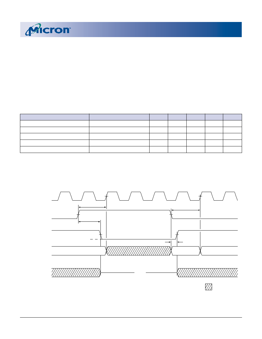
READ/WRITE TIMING
WRITE
D(A1)
1
2
3
4
5
6
7
8
9
CLK
tKHKH
tKLKH
tKHKL
10
CE#
tKHCX
tCVKH
R/W#
CKE#
tKHEX
tEVKH
BWx#
ADV/LD#
tKHAX
tAVKH
ADDRESS
A1
A2
A3
A4
A5
A6
A7
tKHDX
tDVKH
DQ
COMMAND
tKHQX1
D(A1)
D(A2)
Q(A4)
Q(A3)
D(A2+1)
tKHQX
tKHQZ
tKHQV
WRITE
D(A2)
BURST
WRITE
D(A2+1)
READ
Q(A3)
READ
Q(A4)
BURST
READ
Q(A4+1)
WRITE
D(A5)
READ
Q(A6)
WRITE
D(A7)
DESELECT
OE#
tGLQV
tGLQX
tGHQZ
DON'T CARE
UNDEFINED
D(A5)
tKHQX
Q(A4+1)
D(A7)
Q(A6)
-10
-12
SYMBOL
MIN MAX MIN MAX UNITS
t
GHQZ
5.0
5.0
ns
t
AVKH
2.0
2.5
ns
t
EVKH
2.0
2.5
ns
t
CVKH
2.0
2.5
ns
t
DVKH
2.0
2.5
ns
t
KHAX
0.5
0.5
ns
t
KHEX
0.5
0.5
ns
t
KHCX
0.5
0.5
ns
t
KHDX
0.5
0.5
ns
READ/WRITE TIMING PARAMETERS
-10
-12
SYMBOL
MIN MAX MIN MAX UNITS
t
KHKH
10
12
ns
f
KF
100
83
MHz
t
KHKL
3.0
4.0
ns
t
KLKH
3.0
4.0
ns
t
KHQV
7.5
9.0
ns
t
KHQX
3.0
3.0
ns
t
KHQX1
3.0
3.0
ns
t
KHQZ
5.0
5.0
ns
t
GLQV
5.0
5.0
ns
t
GLQX
0
0
ns
NOTE: 1. For this waveform, ZZ is tied LOW.
2. Burst sequence order is determined by MODE (0 = linear, 1 = interleaved). BURST operations are optional.
3. CE# represents three signals. When CE# = 0, it represents CE# = 0, CE2# = 0, CE2 = 1.
4. Data coherency is provided for all possible operations. If a READ is initiated, the most current data is used. The most
recent data may be from the input data register.
16
2Mb: 128K x 18, 64K x 32/36 3.3V I/O, Flow-Through ZBT SRAM
Micron Technology, Inc., reserves the right to change products or specifications without notice.
MT55L128L18F1_C.p65 ≠ Rev. C, Pub. 11/02
©2002, Micron Technology, Inc.
2Mb: 128K x 18, 64K x 32/36
3.3V I/O, FLOW-THROUGH ZBT SRAM
NOT RECOMENDED FOR NEW DESIGNS
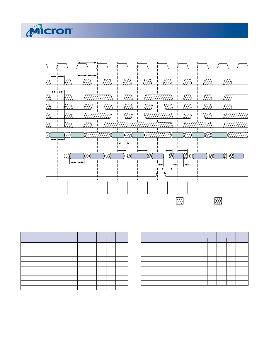
NOP, STALL AND DESELECT CYCLES
READ
Q(A3)
4
5
6
7
8
9
10
A3
A4
A5
D(A4)
1
2
3
CLK
CE#
R/W#
CKE#
BWx#
ADV/LD#
ADDRESS
DQ
COMMAND
WRITE
D(A4)
STALL
WRITE
D(A1)
READ
Q(A2)
STALL
NOP
READ
Q(A5)
DESELECT
CONTINUE
DESELECT
DON'T CARE
UNDEFINED
tKHQZ
A1
A2
Q(A2)
D(A1)
Q(A3)
tKHQX
Q(A5)
NOTE: 1. The IGNORE CLOCK EDGE or STALL cycle (clock 3) illustrates CKE# being used to create a "pause." A WRITE is not
performed during this cycle.
2. For this waveform, ZZ and OE# are tied LOW.
3. CE# represents three signals. When CE# = 0, it represents CE# = 0, CE2# = 0, CE2 = 1.
4. Data coherency is provided for all possible operations. If a READ is initiated, the most current data is used. The most
recent data may be from the input data register.
NOP, STALL AND DESELECT TIMING PARAMETERS
-10
-12
SYMBOL
MIN MAX MIN MAX UNITS
t
KHQX
3.0
3.0
ns
t
KHQZ
5.0
5.0
ns
17
2Mb: 128K x 18, 64K x 32/36 3.3V I/O, Flow-Through ZBT SRAM
Micron Technology, Inc., reserves the right to change products or specifications without notice.
MT55L128L18F1_C.p65 ≠ Rev. C, Pub. 11/02
©2002, Micron Technology, Inc.
2Mb: 128K x 18, 64K x 32/36
3.3V I/O, FLOW-THROUGH ZBT SRAM
NOT RECOMENDED FOR NEW DESIGNS
100-PIN PLASTIC TQFP (JEDEC LQFP)
14.00 ±0.10
1.40 ±0.05
16.00 ±0.20
0.10
+0.10
-0.05
0.15
+0.03
-0.02
22.10
+0.10
-0.20
0.32
+0.06
-0.10
20.10 ±0.10
0.65 TYP
0.625
1.60 MAX
DETAIL A
SEE DETAIL A
0.60 ±0.15
1.00 TYP
GAGE PLANE
0.25
0.10
PIN #1 ID
NOTE:
1. All dimensions in millimeters
MAX
or typical here noted.
MIN
2. Package width and length do not include mold protrusion; allowable mold protrusion is 0.25mm per
side.
8000 S. Federal Way, P.O. Box 6, Boise, ID 83707-0006, Tel: 208-368-3900
E-mail: prodmktg@micron.com, Internet: http://www.micronsemi.com, Customer Comment Line: 800-932-4992
Micron, the M logo, and the Micron logo are trademarks and/or service marks of Micron Technology, Inc.
ZBT and Zero Bus Turnaround are trademarks of Integrated Device Technology, Inc.,
and the architecture is supported by Micron Technology, Inc., and Motorola Inc.
DATA SHEET DESIGNATIONS
No Marking: This data sheet contains minimum and maximum limits specified over the complete power supply
and temperature range for production devices. Although considered final, these specifications are
subject to change, as further product development and data characterization sometimes occur.

18
2Mb: 128K x 18, 64K x 32/36 3.3V I/O, Flow-Through ZBT SRAM
Micron Technology, Inc., reserves the right to change products or specifications without notice.
MT55L128L18F1_C.p65 ≠ Rev. C, Pub. 11/02
©2002, Micron Technology, Inc.
2Mb: 128K x 18, 64K x 32/36
3.3V I/O, FLOW-THROUGH ZBT SRAM
NOT RECOMENDED FOR NEW DESIGNS
REVISION HISTORY
Added "NOT RECOMENDED FOR NEW DESIGNS," REV. C, Pub. 11/02, FINAL ........................ November/20/02
Removed FBGA package, REV 6/01, FINAL ............................................................................................................. June/7/01
Removed FBGA Part Marking Guide, REV 8/00, FINAL ................................................................................. August/22/00
Changed FBGA capacitance values, REV 8/00, FINAL ...................................................................................... August/7/00
C
I
; TYP 2.5pF from 4pF; MAX. 3.5pF from 5pF
C
O
; TYP 4pF from 6pF; MAX. 5pF from 7pF
C
CK
; TYP 2.5pF from 5pF; MAX. 3.5pF from 6pF
Removed IT References, REV 7/00, FINAL ............................................................................................................. July/10/00
Added FBGA Part Marking Guide
Removed IT from Part Number Example, REV 6/00, FINAL .............................................................................. June/21/00
Added # of datalines to the databus in the Block Diagrams
Added Note - "Preliminary Package Data" to FBGA Capacitance and Thermal Resistance Tables
Changed heading on Mechanical Drawing from BGA to FBGA
Added 165-Pin FBGA package, REV 5/00, FINAL ................................................................................................. May/23/00
Added PRELIMINARY PACKAGE DATA to diagram