Document Outline
- Features/Options
- Valid Part Numbers
- General Description
- General Description (continued)
- DDR Operation
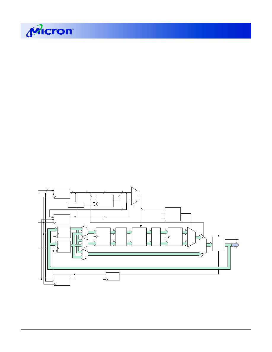
- Functional Block Diagram, 256K x 36
- DDR Operation (continued)
- Programmable Impedance Output Buffer
- Clocking
- Application Example
- Ball Assignment (Top View), 165-Ball FBGA
- Ball Descriptions
- Ball Descriptions (continued)
- Linear Burst Address Table
- Bus Cycle State Diagram
- Truth Table
- Absolute Maximum Ratings
- DC Electrical Characteristics and Operating Conditions
- AC Electrical Characteristics and Operating Conditions
- IDD Operating Conditions and Maximum Limits
- Capacitance
- Thermal Resistance
- AC Electrical Characteristics
- AC Test Conditions
- Figure 1, Output Load Equivalent
- READ/WRITE Timing
- IEEE 1149.1 Serial Boundary Scan (JTAG)
- Disabling the JTAG Feature
- Test Access Port (TAP)
- Test Clock (TCK)
- Test Mode Select (TMS)
- Test Data-In (TDI)
- Figure 2, TAP Controller State Diagram
- Test Data-Out (TDO)
- Performing a TAP RESET
- Tap Registers
- Instruction Register
- Bypass Register
- Boundary Scan Register
- Figure 3, TAP Controller Block Diagram
- Identification (ID) Register
- TAP Instruction Set
- Overview
- EXTEST
- IDCODE
- SAMPLE Z
- SAMPLE/PRELOAD
- BYPASS
- Reserved
- TAP Timing
- TAP AC Electrical Characteristics
- TAP AC Test Conditions
- Figure 4, TAP AC Output Load Equivalent
- TAP DC Electrical Characteristics and Operating Conditions
- Identification Register Definitions
- Scan Register Sizes
- Instruction Codes
- Boundary Scan (Exit) Order
- 165-Ball FBGA Package Drawing
1
256K x 36 2.5V V
DD
, HSTL, Pipelined DDR SRAM
©2002, Micron Technology, Inc.
MT57V256H36P_5.p65 ≠ Rev. 5, Pub. 5/02
256K x 36
2.5V V
DD
, HSTL, PIPELINED DDR SRAM
PRODUCTS AND SPECIFICATIONS DISCUSSED HEREIN ARE SUBJECT TO CHANGE BY MICRON WITHOUT NOTICE.
9Mb
DDR SRAM
FEATURES
∑ Fast cycle times: 5ns and 6ns
∑ 256K x 36 configuration
∑ Pipelined double data rate operation
∑ Single +2.5V ±0.1V power supply (V
DD
)
∑ Separate isolated output buffer supply (V
DD
Q)
∑ JEDEC-standard HSTL I/O
∑ User-selectable trip point with V
REF
∑ HSTL programmable impedance outputs synchro-
nized to optional dual data clocks
∑ Echo clock outputs
∑ JTAG boundary scan
∑ Fully static design for reduced-power standby
∑ Clock-stop capability
∑ Common data inputs and data outputs
∑ Low control ball count
∑ Internally self-timed, registered LATE WRITE cycle
∑ Linear burst order with four-tick burst counter
∑ 13 x 15mm, 1mm pitch, 11 x 15 grid FBGA package
∑ Full data coherency, providing most current data
OPTIONS
MARKING*
∑ Clock Cycle Timing
5ns (200 MHz)
-5
6ns (167 MHz)
-6
∑ Configuration
256K x 36
MT57V256H36P
∑ Package
165-ball, 13mm x 15mm FBGA
F
* A Part Marking Guide for the FBGA devices can be found on Micron's
Web site--
http://www.micron.com/numberguide.
165-Ball FBGA
MT57V256H36P
GENERAL DESCRIPTION
The MicronÆ DDR Synchronous SRAM employs high-
speed, low-power CMOS designs using an advanced 6T
CMOS process.
The DDR SRAM integrates a 9Mb SRAM core with
advanced synchronous peripheral circuitry and a 2-bit
burst counter. All synchronous inputs pass through reg-
isters controlled by an input clock pair (K and K#) and are
VALID PART NUMBERS
PART NUMBER
DESCRIPTION
MT57V256H36PF-xx
256K x 36, HSTL, DDR, Pipelined
latched on the rising edge of K and K#. The synchronous
inputs include all addresses, all data inputs, active LOW
load (LD#) and read/write (R/W#). Write data is regis-
tered on the rising edges of both K and K#. Read data is
driven on the rising edge of C and C# if provided, or on the
rising edge of K and K# if C and C# are not provided.
Asynchronous inputs include impedance match (ZQ).
Synchronous data outputs (Q) are closely matched to the
two echo clocks (CQ and CQ#), which can be used as data
receive clocks. Output data clocks (C, C#) are also pro-
vided for maximum system clocking and data synchroni-
zation flexibility.
Additional write registers are incorporated to enhance
pipelined WRITE cycles and reduce READ-to-WRITE turn-
around time. WRITE cycles are self-timed.
The device does not utilize internal phase-locked loops
and can therefore be placed into a stopped-clock state to
minimize power without lengthy restart times.
Four balls are used to implement JTAG test capabili-
ties: test mode select (TMS), test data-in (TDI), test clock
(TCK) and test data-out (TDO). JTAG circuitry is used to
serially shift data to and from the SRAM. JTAG inputs use
JEDEC-standard 2.5V I/O levels to shift data during this
testing mode of operation.
The device can be used in HSTL systems by supplying
an appropriate reference voltage (V
REF
). The device is
2
256K x 36 2.5V V
DD
, HSTL, Pipelined DDR SRAM
Micron Technology, Inc., reserves the right to change products or specifications without notice.
MT57V256H36P_5.p65 ≠ Rev. 5, Pub. 5/02
©2002, Micron Technology, Inc.
256K x 36
2.5V V
DD
, HSTL, PIPELINED DDR SRAM
NOTE: 1. SA0 and SA1 are advanced in linear burst order at each K and K# rising edge.
2. The compare width is a 16-bits. The compare is performed only if a WRITE is pending and a READ cycle is requested. If
the address matches, data is routed directly to the device outputs, bypassing the memory array.
3. The functional block diagram illustrates simplified device operation. See truth table, ball descriptions, and timing
diagrams for detailed information.
4. CQ, CQ# do not tristate except during some JTAG test modes.
ideally suited for applications requiring very rapid data
transfer by operation in data-doubled mode. The device
is also ideal in applications requiring the cost benefits of
pipelined CMOS SRAMs and the reduced READ-to-WRITE
turnaround times of Late Write SRAMs.
The SRAM operates from a +2.5V power supply, and
all inputs and outputs are HSTL-compatible. The device
is ideally suited for cache, network, telecom, DSP, and
other applications that benefit from a very wide, high-
speed data bus.
Please refer to Micron's Web site (
www.micron.com/
sramds
) for the latest data sheet.
DDR OPERATION
The DDR SRAM enables high performance operation
through high clock frequencies (achieved through pipe-
lining) and double data rate mode of operation. At slower
frequencies, the DDR SRAM requires a single NO OPERA-
TION (NOP) cycle when transitioning from a READ to a
WRITE cycle. At higher frequencies, a second NOP cycle
may be required to prevent bus contention. NOP cycles
GENERAL DESCRIPTION (continued)
are not required when switching from a WRITE to a
READ.
If a READ occurs after a WRITE cycle, address and
data for the WRITE are stored in registers. The write
information must be stored because the SRAM cannot
perform the last WORD WRITE to the array without con-
flicting with the READ. The data stays in this register until
the next WRITE cycle occurs. On the first WRITE cycle
after the READ(s), the stored data from the earlier WRITE
will be written into the SRAM array. This is called a
POSTED WRITE.
A READ can be made immediately to an address even
if that address was written in the previous cycle. During
this READ cycle, the SRAM array is bypassed, and data is
read instead from the data register storing the recently
written data. This is transparent to the user. This feature
facilitates system data coherency.
The DDR SRAM differs in some ways from its prede-
cessor, the Claymore DDR SRAM. Single data rate opera-
tion is not supported, hence no SD/DD# ball is provided.
Only bursts of four are supported. In addition to the echo
FUNCTIONAL BLOCK DIAGRAM
256K x 36
36
36
SA0, SA1, SA
LD#
ADDRESS
REGISTER
18
18
18
18
16
18
WRITE
ADDRESS
REGISTER
DQ
36
OUTPUT
BUFFER
BURST
LOGIC
SA0'
SA0'
SA1'
D1
D0
Q1
Q0
SA0
SA1
(NOTE 1)
36
36
INPUT
REGISTER
36
36
36
36
36
(NOTE 2)
K
K#
R/W#
REGISTER
OE
REGISTER
R/W#
COMPARE
E
E
E
CLK
WRITE#
18
WRITE#
E
E
INPUT
REGISTER
E
C
SA0'''
WRITE#
READ
SA0''
SA0'''
SA1'-SA17'
ZQ
0
1
SA0#'
SA0'
SA0#'
SA0'
OUTPUT
CONTROL
LOGIC
C
C#
36
36
36
36
36
36
36
36
36
36
36
OUTPUT
REGISTER
WRITE
REGISTER
SENSE
AMPS
128K x 72
MEMORY
ARRAY
WRITE
DRIVER
C
CLK
2:1
MUX
0
1
CQ, CQ#

3
256K x 36 2.5V V
DD
, HSTL, Pipelined DDR SRAM
Micron Technology, Inc., reserves the right to change products or specifications without notice.
MT57V256H36P_5.p65 ≠ Rev. 5, Pub. 5/02
©2002, Micron Technology, Inc.
256K x 36
2.5V V
DD
, HSTL, PIPELINED DDR SRAM
clocks, two single-ended input clocks are available (C,
C#). The SRAM synchronizes its output data to these data
clock rising edges if provided. If not present, C and C#
must be tied high and output timing is derived from K
and K#. No differential clocks are used in this device. This
clocking scheme provides greater system tuning capabil-
ity than Claymore SRAMs and reduces the number of
input clocks required by the bus master.
PROGRAMMABLE IMPEDANCE OUTPUT
BUFFER
The DDR SRAM is equipped with programmable im-
pedance output buffers. This allows a user to match the
driver impedance to the system. To adjust the imped-
ance, an external precision resistor (RQ) is connected
between the ZQ ball and V
SS
. The value of the resistor
must be five times the desired impedance. For example,
a 350
W resistor is required for an output impedance of
70
W. To ensure that output impedance is one fifth the
value of RQ (within 10 percent), the range of RQ is 175
W
to 350
W. Alternately, the ZQ ball can be connected di-
rectly to V
DD
Q, which will place the device in a minimum
impedance mode.
Output impedance updates may be required because
variations may occur in supply voltage and temperature
over time. The device samples the value of RQ. An update
DDR OPERATION (continued)
of the impedance is transparent to the system. Imped-
ance updates do not affect device operation, and all data
sheet timing and current specifications are met during
an update.
The device will power up with an output impedance
set at 50
W. To guarantee optimum output driver imped-
ance after power-up, the SRAM needs 1,024 cycles to
update the impedance. The user can operate the part
with fewer than 1,024 clock cycles, but optimal output
impedance is not guaranteed.
CLOCKING
The DDR SRAM supports flexible clocking approaches.
C and C# may be supplied to the SRAM to synchronize
data output across multiple devices, enabling the bus
master to receive all data simultaneously. If C and C# are
not provided (tied HIGH) K and K# are used as the output
timing reference. The echo clocks (CQ and CQ#) provide
another alternative for data synchronization. The echo
clocks are controlled exactly like the DQ signals except
that CQ and CQ# have an additional small delay for easier
data capture by the bus master. Echo clocks must be
separately received for each SRAM in the system. Use of
echo clocks maximizes the available data window for
each SRAM in the system.
LD#
Vterm = 0.75V
Vterm = 0.75V
C C#
R/W#
ZQ
K#
DQn
SAn
K
LD#
C C#
R/W#
ZQ
K#
DQn
SAn
K
BUS
MASTER
(CPU
or
ASIC)
SRAM
SRAM
DQ
Addresses
Cycle Start#
R/W#
Return CLK
Source CLK
Return CLK#
Source CLK#
R = 50
R = 250
R = 250
APPLICATION EXAMPLE
4
256K x 36 2.5V V
DD
, HSTL, Pipelined DDR SRAM
Micron Technology, Inc., reserves the right to change products or specifications without notice.
MT57V256H36P_5.p65 ≠ Rev. 5, Pub. 5/02
©2002, Micron Technology, Inc.
256K x 36
2.5V V
DD
, HSTL, PIPELINED DDR SRAM
*Expansion addresses: 9A for 18Mb, 3A for 36Mb, 10A for 72Mb, 2A for 144Mb.
BALL ASSIGNMENT (Top View)
165-Ball FBGA
1
2
3
4
5
6
7
8
9
10
11
A
CQ#
V
SS
/
SA
*
NC/
SA
*
R/W#
NC
K#
NC
LD#
NC/
SA
*
V
SS
/
SA
*
CQ
B
NC
DQ19
DQ18
SA
NC
K
NC
SA
NC
NC
DQ17
C
NC
NC
DQ20
V
SS
SA
SA0
SA1
V
SS
NC
DQ15
DQ16
D
NC
DQ22
DQ21
V
SS
V
SS
V
SS
V
SS
V
SS
NC
NC
DQ14
E
NC
NC
DQ23
V
DD
Q
V
SS
V
SS
V
SS
V
DD
Q
NC
DQ12
DQ13
F
NC
DQ25
DQ24
V
DD
Q
V
DD
V
SS
V
DD
V
DD
Q
NC
NC
DQ11
G
NC
DQ26
DQ27
V
DD
Q
V
DD
V
SS
V
DD
V
DD
Q
NC
NC
DQ10
H
NC
V
REF
V
DD
Q
V
DD
Q
V
DD
V
SS
V
DD
V
DD
Q
V
DD
Q
V
REF
ZQ
J
NC
NC
DQ28
V
DD
Q
V
DD
V
SS
V
DD
V
DD
Q
NC
DQ9
DQ8
K
NC
NC
DQ29
V
DD
Q
V
DD
V
SS
V
DD
V
DD
Q
NC
DQ6
DQ7
L
NC
DQ31
DQ30
V
DD
Q
V
SS
V
SS
V
SS
V
DD
Q
NC
NC
DQ5
M
NC
NC
DQ32
V
SS
V
SS
V
SS
V
SS
V
SS
NC
DQ3
DQ4
N
NC
DQ34
DQ33
V
SS
SA
SA
SA
V
SS
NC
NC
DQ2
P
NC
NC
DQ35
SA
SA
C
SA
SA
NC
DQ0
DQ1
R
TDO
TCK
SA
SA
SA
C#
SA
SA
SA
TMS
TDI

5
256K x 36 2.5V V
DD
, HSTL, Pipelined DDR SRAM
Micron Technology, Inc., reserves the right to change products or specifications without notice.
MT57V256H36P_5.p65 ≠ Rev. 5, Pub. 5/02
©2002, Micron Technology, Inc.
256K x 36
2.5V V
DD
, HSTL, PIPELINED DDR SRAM
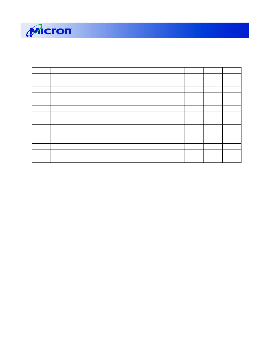
BALL DESCRIPTIONS
BALL
SYMBOL
TYPE
DESCRIPTION
6C
SA0
Input
Synchronous Address Inputs: These inputs are registered and must
7C
SA1
meet the setup and hold times around the rising edge of K. Balls
4B, 8B, 5C,
SA
9A, 3A, 10A, and 2A are reserved for the next higher-order address
5N-7N, 4P, 5P,
inputs on 18, 36, 72, and 144Mb devices, respectively. SA0 and
7P, 8P, 3R-5R,
SA1 are used as the lowest two address bits for BURST READ and
7R-9R
BURST WRITE operations. These inputs are ignored when device is
deselected or once BURST operation is in progress.
8A
LD#
Input
Synchronous Load: This input is brought LOW when a bus cycle
sequence is to be defined. This definition includes address and
read/write direction. All transactions operate on a burst of 4 data
(two clock periods of bus activity).
4A
R/W#
Input
Synchronous Read/Write Input: When LD# is LOW, this input
designates the access type (READ when R/W# is HIGH, WRITE when
R/W# is LOW) for the loaded address. R/W# must meet the setup
and hold times around the rising edge of K.
6B
K
Input
Input Clock: This input clock pair registers address and control
6A
K#
inputs on the rising edge of K, and registers data on the rising
edge of K and the rising edge of K#. K# is ideally 180 degrees out
of phase with K. All synchronous inputs must meet setup and hold
times around the clock rising edges.
6P
C
Input
Output Clock: This clock pair provides a user controlled means of
6R
C#
tuning device output data. The rising edge of C is used as the
output timing reference for first and third output data. The rising
edge of C# is used as the output reference for second and fourth
output data. Ideally, C# is 180 degrees out of phase with C. C and
C# may be tied HIGH to force the use of K and K# as the output
reference clocks instead of having to provide C and C# clocks. If
tied HIGH, C and C# must remain HIGH and not be toggled during
device operation.
11H
ZQ
Input
Output Impedance Matching Input: This input is used to tune the
device outputs to the system data bus impedance. DQ and CQ
output impedance are set to 0.2 x RQ, where RQ is a resistor from
this bump to ground. Alternately, this ball can be connected
directly to V
DD
Q, which enables the minimum impedance mode.
This ball cannot be connected directly to GND or left unconnected.
10R
TMS
Input
IEEE 1149.1 Test Inputs: JEDEC-standard 2.5V I/O levels. These balls
11R
TDI
may be left Not Connected if the JTAG function is not used in the
circuit.
2R
TCK
Input
IEEE 1149.1 Clock Input: JEDEC-standard 2.5V I/O levels. This ball
must be tied to V
SS
if the JTAG function is not used in the circuit.
2H, 10H
V
REF
Input
HSTL Input Reference Voltage: Nominally V
DD
Q/2. Provides a
reference voltage for the input buffers.
(continued on next page)