 | –≠–ª–µ–∫—Ç—Ä–æ–Ω–Ω—ã–π –∫–æ–º–ø–æ–Ω–µ–Ω—Ç: HAL401SO | –°–∫–∞—á–∞—Ç—å:  PDF PDF  ZIP ZIP |

HAL401
Linear Hall Effect
Sensor IC
Edition June 26, 2002
6251-470-1DS
DATA SHEET
MICRONAS
MICRONAS

HAL401
DATA SHEET
Freigabe-Exemplar
2
Micronas
Contents
Page
Section
Title
3
1.
Introduction
3
1.1.
Features
3
1.2.
Marking Code
3
1.2.1.
Special Marking of Prototype Parts
3
1.3.
Operating Junction Temperature Range
3
1.4.
Hall Sensor Package Codes
3
1.5.
Solderability
4
2.
Functional Description
5
3.
Specifications
5
3.1.
Outline Dimensions
5
3.2.
Dimensions of Sensitive Area
5
3.3.
Positions of Sensitive Areas
5
3.4.
Absolute Maximum Ratings
6
3.4.1.
Storage, Moisture Sensitivity Class and Shelf Life
6
3.5.
Recommended Operating Conditions
7
3.6.
Electrical and Magnetic Characteristics
14
4.
Application Notes
14
4.1.
Ambient Temperature
14
4.2.
EMC and ESD
14
4.3.
Application Circuit
16
5.
Data Sheet History

HAL401
DATA SHEET
Freigabe-Exemplar
3
Micronas
Linear Hall Effect Sensor IC
in CMOS technology
1. Introduction
The HAL 401 is a Linear Hall Effect Sensor produced in
CMOS technology. The sensor includes a temperature-
compensated Hall plate with choppered offset com-
pensation, two linear output stages, and protection de-
vices (see Fig. 2≠1).
The output voltage is proportional to the magnetic flux
density through the hall plate. The choppered offset
compensation leads to stable magnetic characteristics
over supply voltage and temperature.
The HAL 401 can be used for magnetic field measure-
ments, current measurements, and detection of any me-
chanical movement. Very accurate angle measure-
ments or distance measurements can also be done. The
sensor is very robust and can be used in electrical and
mechanical hostile environments.
The sensor is designed for industrial and automotive ap-
plications and operates in the ambient temperature
range from ≠40
∞
C up to 150
∞
C and is available in the
SMD-package SOT-89B.
1.1. Features:
≠ switching offset compensation at 147 kHz
≠ low magnetic offset
≠ extremely sensitive
≠ operates from 4.8 to 12 V supply voltage
≠ wide temperature range T
A
= ≠40
∞
C to +150
∞
C
≠ overvoltage protection
≠ reverse voltage protection of V
DD
-pin
≠ differential output
≠ accurate absolute measurements of DC and low fre-
quency magnetic fields
≠ on-chip temperature compensation
1.2. Marking Code
Type
Temperature Range
A
K
HAL401
401A
401K
1.2.1. Special Marking of Prototype Parts
Prototype parts are coded with an underscore beneath the
temperature range letter on each IC. They may be used
for lab experiments and design-ins but are not intended to
be used for qualification tests or as production parts.
1.3. Operating Junction Temperature Range
The Hall sensors from Micronas are specified to the chip
temperature (junction temperature T
J
).
A: T
J
= ≠40
∞
C to +170
∞
C
K: T
J
= ≠40
∞
C to +140
∞
C
Note: Due to the high power dissipation at high current
consumption, there is a difference between the ambient
temperature (T
A
) and junction temperature. Please refer
section 4.1. on page 14 for details.
1.4. Hall Sensor Package Codes
Type: 401
HAL XXXPA-T
Temperature Range: A or K
Package: SF for SOT-89B
Type: 401
Package: SOT-89B
Temperature Range: T
J
= ≠40
∞
C to +140
∞
C
Example: HAL 401SF-K
Hall sensors are available in a wide variety of packaging
versions and quantities. For more detailed information,
please refer to the brochure: "Ordering Codes for Hall
Sensors".
1.5. Solderability
all packages: according to IEC68-2-58
During soldering reflow processing and manual rework-
ing, a component body temperature of 260
∞
C should not
be exceeded.
Components stored in the original packaging should
provide a shelf life of at least 12 months, starting from the
date code printed on the labels, even in environments as
extreme as 40
∞
C and 90% relative humidity.
OUT1
GND
2
4
1 V
DD
Fig. 1≠1: Pin configuration
OUT2
3
HAL401
DATA SHEET
Freigabe-Exemplar
4
Micronas
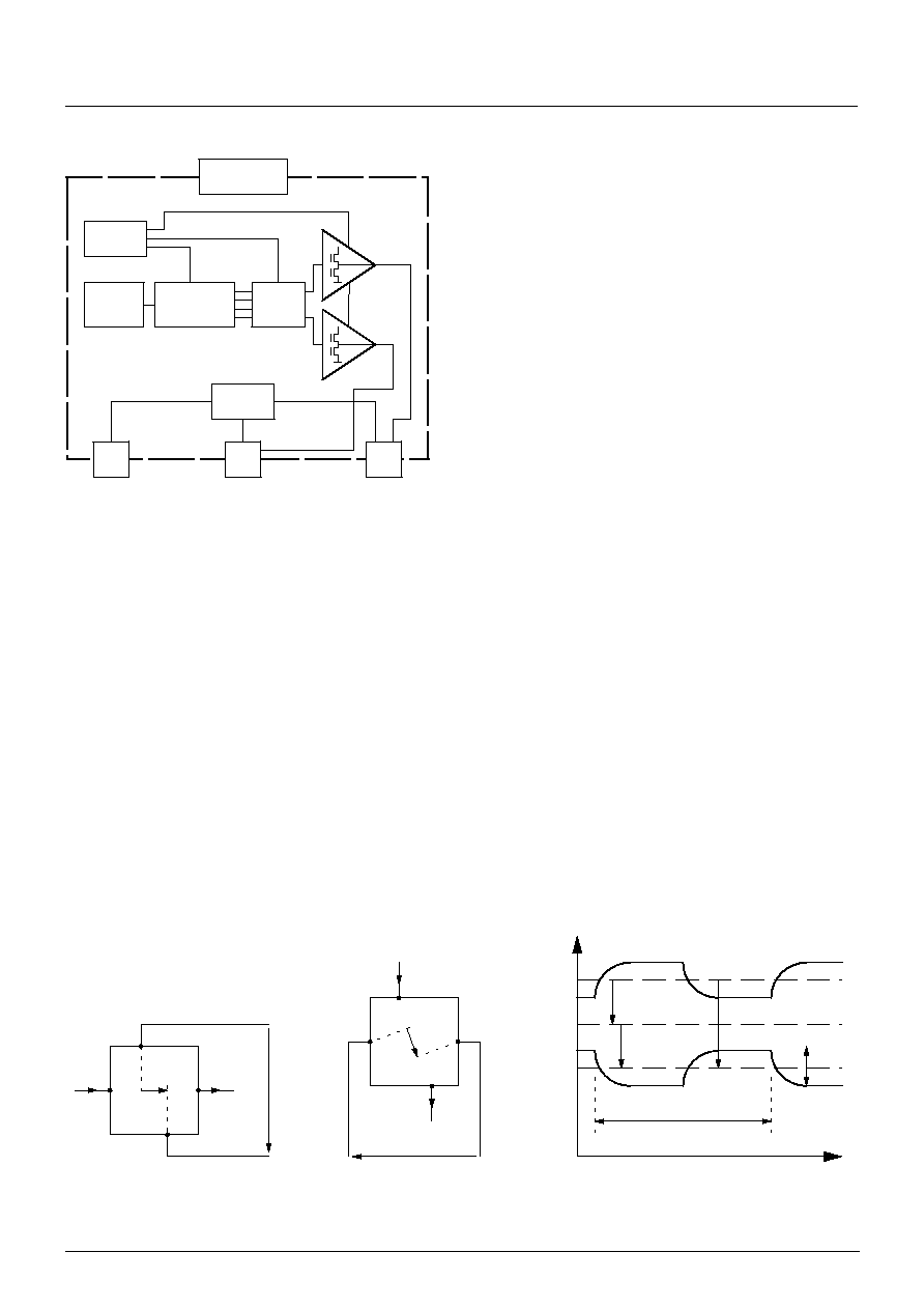
2. Functional Description
Temp.
Dependent
Bias
Offset
Compensation;
Hallplate
Switching
Matrix
1
4
2
3
OUT1
OUT2
Fig. 2≠1: Block diagram of the HAL 401 (top view)
V
DD
Protection
Device
Chopper
Oscillator
GND
The Linear Hall Sensor measures constant and low fre-
quency magnetic flux densities accurately. The differen-
tial output voltage V
OUTDIF
(difference of the voltages on
pin 2 and pin 3) is proportional to the magnetic flux densi-
ty passing vertically through the sensitive area of the
chip. The common mode voltage V
CM
(average of the
voltages on pin 2 and pin 3) of the differential output am-
plifier is a constant 2.2 V.
The differential output voltage consists of two compo-
nents due to the switching offset compensation tech-
nique. The average of the differential output voltage rep-
resents the magnetic flux density. This component is
overlaid by a differential AC signal at a typical frequency
of 147 kHz. The AC signal represents the internal offset
voltages of amplifiers and hall plates that are influenced
by mechanical stress and temperature cycling.
External filtering or integrating measurement can be
done to eliminate the AC component of the signal. Re-
sultingly, the influence of mechanical stress and temper-
ature cycling is suppressed. No adjustment of magnetic
offset is needed.
The sensitivity is stabilized over a wide range of temper-
ature and supply voltage due to internal voltage regula-
tion and circuits for temperature compensation.
Offset Compensation (see Fig. 2≠2)
The Hall Offset Voltage is the residual voltage measured
in absence of a magnetic field (zero-field residual volt-
age). This voltage is caused by mechanical stress and
can be modeled by a displacement of the connections
for voltage measurement and/or current supply.
Compensation of this kind of offset is done by cyclic
commutating the connections for current flow and volt-
age measurement.
≠ First cycle:
The hall supply current flows
between points 4 and 2.
In the absence of a magnetic field, V
13
is the Hall Off-
set Voltage (+V
Offs
). In case of a magnetic field, V
13
is
the sum of the Hall voltage (V
H
) and V
Offs
.
V
13
= V
H
+ V
Offs
≠ Second cycle:
The hall supply current flows between points 1 and 3.
In the absence of a magnetic field, V
24
is the Hall Off-
set Voltage with negative polarity (≠V
Offs
). In case of
a magnetic field, V
24
is the difference of the Hall volt-
age (V
H
) and V
Offs
.
V
24
= V
H
≠ V
Offs
In the first cycle, the output shows the sum of the Hall
voltage and the offset; in the second, the difference of
both. The difference of the mean values of V
OUT1
and
V
OUT2
(V
OUTDIF
) is equivalent to V
Hall
.
Fig. 2≠2: Hall Offset Compensation
Note: The numbers do not
represent pin numbers.
I
C
2
4
V
Offs
1
3
V
I
C
2
4
V
Offs
1
3
V
V
t
V
CM
for B
u
0 mT
V
OUT1
V
OUT2
V
OUTDIF
V
OUTDIF/2
V
OUTDIF/2
1/f
CH
= 6.7
µ
s
V
OUTAC
a) Offset Voltage
b) Switched Current Supply
c) Output Voltage
HAL401
DATA SHEET
Freigabe-Exemplar
5
Micronas
3. Specifications
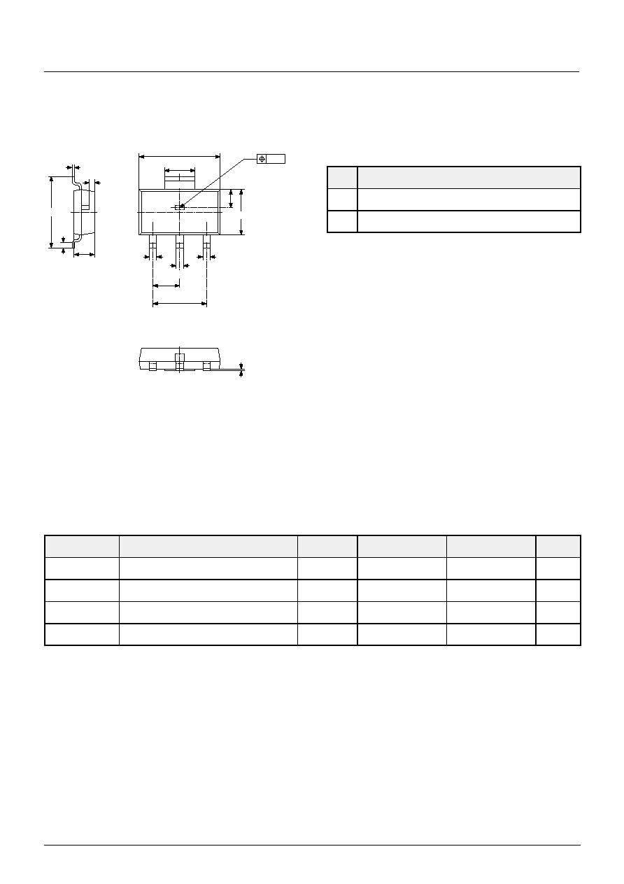
3.1. Outline Dimensions
Fig. 3≠1:
Plastic Small Outline Transistor Package
(SOT-89B)
Weight approximately 0.035 g
Dimensions in mm
4.55
1.7
min.
0.25
2.55
0.4
0.4
0.4
1.5
3.0
0.06
±
0.04
branded side
SPGS0022-5-A3/2E
y
1
2
3
4
±
0.2
0.15
0.3
2
0.2
sensitive area
top view
1.15
3.2. Dimensions of Sensitive Area
0.37 mm x 0.17 mm
3.3. Positions of Sensitive Areas
SOT-89B
x
center of the package
y
0.95 mm nominal
Note: For all package diagrams, a mechanical tolerance
of
±
0.05 mm applies to all dimensions where no tolerance
is explicitly given.
3.4. Absolute Maximum Ratings
Symbol
Parameter
Pin No.
Min.
Max.
Unit
V
DD
Supply Voltage
1
≠12
12
V
V
O
Output Voltage
2, 3
≠0.3
12
V
I
O
Continuous Output Current
2, 3
≠5
5
mA
T
J
Junction Temperature Range
≠40
170
∞
C
Stresses beyond those listed in the "Absolute Maximum Ratings" may cause permanent damage to the device. This
is a stress rating only. Functional operation of the device at these or any other conditions beyond those indicated in the
"Recommended Operating Conditions/Characteristics" of this specification is not implied. Exposure to absolute maxi-
mum ratings conditions for extended periods may affect device reliability.
HAL401
DATA SHEET
Freigabe-Exemplar
6
Micronas
3.4.1. Storage, Moisture Sensitivity Class,
and Shelf Life
Storage has no influence on the electrical and magnetic
characteristics of the sensors. However, under disad-
vantageous conditions, extended storage time can lead
to alteration of the lead plating, which affects the solder-
ing process.
Moisture Sensitivity Class:
The package SOT-89B achieves level 1 according to
J-STD-020A "Moisture/Reflow Sensitivity Classification
for Non-hermetic Solid State Surface Mount Devices". If
the sensors are stored at maximum 30
∞
C and maximum
90% relative humidity no Dry Pack is required.
The permissible storage time (shelf life) of the sensors
would be minimum 12 months, beginning from the date
of manufacturing, if they are stored in the original pack-
aging at maximum 40
∞
C ambient temperature and max-
imum 90% relative humidity.
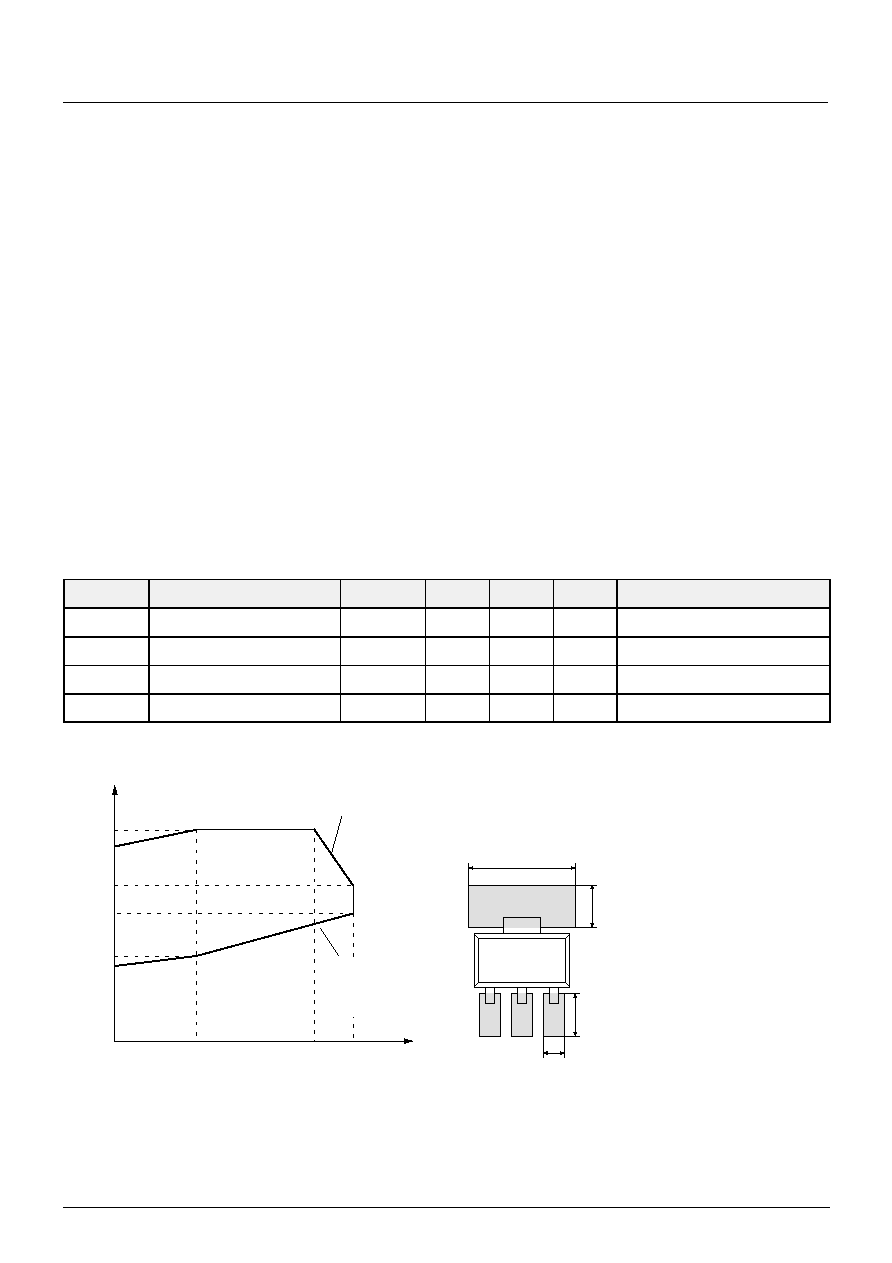
3.5. Recommended Operating Conditions
Symbol
Parameter
Pin No.
Min.
Max.
Unit
Remarks
I
O
Continuous Output Current
2, 3
≠2.25
2.25
mA
T
J
= 25
∞
C
I
O
Continuous Output Current
2, 3
≠1
1
mA
T
J
= 170
∞
C
C
L
Load Capacitance
2, 3
≠
1
nF
B
Magnetic Field Range
≠50
50
mT
»»»»»»»»»»»»
»»»»»»»»»»»»
»»»»»»»»»»»»
»»»»»»»»»»»»
»»»»»»»»»»»»
»»»»»»»»»»»»
»»»»»»»»»»»»
Fig. 3≠2: Recommended Operating Supply Voltage
12 V
6.8 V
4.8 V
≠40
∞
C
25
∞
C
150
∞
C
125
∞
C
V
DD
T
A
power dissipation limit
min. V
DD
for specified
sensitivity
4.5 V
8.0 V
11.5 V
Fig. 3≠3: Recommended pad size SOT-89B
Dimensions in mm
5.0
2.0
2.0
1.0

HAL401
DATA SHEET
Freigabe-Exemplar
7
Micronas
3.6. Electrical and Magnetic Characteristics
at Recommended Operation Conditions (Fig. 3≠2 for T
A
and V
DD
) as not otherwise specified in the column "Conditions".
Typical characteristics for T
J
= 25
∞
C, V
DD
= 6.8 V and ≠50 mT < B < 50 mT
Symbol
Parameter
Pin No.
Min.
Typ.
Max.
Unit
Conditions
I
DD
Supply Current
1
11
14.5
17.1
mA
T
J
= 25
∞
C, I
OUT1,2
= 0 mA
I
DD
Supply Current over
Temperature Range
1
9
14.5
18.5
mA
I
OUT1,2
= 0 mA
V
CM
Common Mode Output Voltage
V
CM
= (V
OUT1
+ V
OUT2
) / 2
2, 3
2.1
2.2
2.3
V
I
OUT1,2
= 0 mA,
CMRR
Common Mode Rejection Ratio
2, 3
≠2.5
0
2.5
mV/V
I
OUT1,2
= 0 mA,
CMRR is limited by the influ-
ence of power dissipation.
S
B
Differential Magnetic Sensitivity
2≠3
42
48.5
55
mV/mT
≠50 mT < B < 50 mT
T
J
= 25
∞
C
S
B
Differential Magnetic Sensitivity
over Temperature Range
2≠3
37.5
46.5
55
mV/mT
≠50 mT < B < 50 mT
B
offset
Magnetic Offset
over Temperature
2≠3
≠1.5
≠0.2
1.5
mT
B = 0 mT, I
OUT1,2
= 0 mA
B
OFFSET
/
T
Magnetic Offset Change
≠25
0
25
µ
T/K
B = 0 mT, I
OUT1,2
= 0 mA
BW
Bandwidth (≠3 dB)
2≠3
≠
10
≠
kHz
without external Filter
1)
NL
dif
Non-Linearity
of Differential Output
2≠3
≠
0.5
2
%
≠50 mT < B < 50 mT
NL
single
Non-Linearity
of Single Ended Output
2, 3
≠
2
≠
%
f
CH
Chopper Frequency over Temp.
2, 3
≠
147
≠
kHz
V
OUTACpp
Peak-to-Peak
AC Output Voltage
2, 3
≠
0.6
1.3
V
n
meff
Magnetic RMS Differential
Broadband Noise
2≠3
≠
10
≠
µ
T
BW = 10 Hz to 10 kHz
f
Cflicker
Corner Frequency
of 1/f Noise
2≠3
≠
10
≠
Hz
B = 0 mT
f
Cflicker
Corner Frequency
of 1/f Noise
2≠3
≠
100
≠
Hz
B = 50 mT
R
OUT
Output Impedance
2, 3
≠
30
50
I
OUT1,2
v
2.5 mA,
T
J
= 25
∞
C, V
DD
= 6.8 V
R
OUT
Output Impedance
over Temperature
2, 3
≠
30
150
I
OUT1,2
v
2.5 mA
R
thJSB
case
Thermal Resistance Junction to
Substrate Backside
≠
150
200
K/W
Fiberglass Substrate
30 mm x 10 mm x 1.5 mm
pad size see Fig. 3≠3
1)
with external 2 pole filter (f
3db
= 5 kHz), V
OUTAC
is reduced to less than 1 mV by limiting the bandwith
HAL401
DATA SHEET
Freigabe-Exemplar
8
Micronas
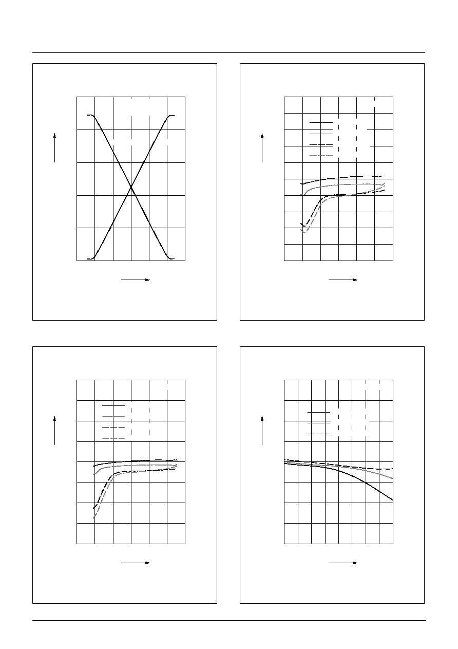
0
1
2
3
4
5
≠150 ≠100
≠50
0
50
100
150 mT
V
B
V
OUT1
V
OUT2
V
OUT1
V
OUT2
Fig. 3≠4: Typical output voltages
versus magnetic flux density
T
A
= 25
∞
C
V
DD
= 6.8 V
≠2
≠1.5
≠1.0
≠0.5
0.0
0.5
1.0
1.5
2.0
2
4
6
8
10
12
14 V
mT
V
DD
B
OFFS
B = 0 mT
Fig. 3≠5: Typical magnetic offset of
differential output versus supply voltage
T
A
= ≠40
∞
C
T
A
= 25
∞
C
T
A
= 125
∞
C
T
A
= 150
∞
C
≠0.05
≠0.04
≠0.03
≠0.02
≠0.01
0.00
0.01
0.02
0.03
0.04
0.05
2
4
6
8
10
12
14 V
V
V
DD
V
OFFS
B = 0 mT
Fig. 3≠6: Typical differential output offset
voltage versus supply voltage
T
A
= ≠40
∞
C
T
A
= 25
∞
C
T
A
= 125
∞
C
T
A
= 150
∞
C
≠2
≠1.5
≠1.0
≠0.5
0.0
0.5
1.0
1.5
2.0
≠50 ≠25
0
25
50
75 100 125 150
∞
C
mT
T
A
B
OFFS
B = 0 mT
Fig. 3≠7: Typical magnetic offset of differential
output versus ambient temperature
V
DD
= 4.8 V
V
DD
= 6.0 V
V
DD
= 12 V

HAL401
DATA SHEET
Freigabe-Exemplar
9
Micronas
15
20
25
30
35
40
45
50
55
60
2
4
6
8
10
12
14 V
mV/mT
V
DD
S
B
B =
±
50 mT
Fig. 3≠8: Typical differential magnetic
sensitivity versus supply voltage
T
A
= ≠40
∞
C
T
A
= 25
∞
C
T
A
= 125
∞
C
T
A
= 150
∞
C
≠1.5
≠1.0
≠0.5
0.0
0.5
1.0
1.5
≠80 ≠60 ≠40 ≠20
0
20
40
60
80 mT
%
B
NL
dif
T
A
= 25
∞
C
Fig. 3≠9: Typical non-linearity of differential
output versus magnetic flux density
V
DD
= 4.8 V
V
DD
= 6.0 V
V
DD
= 12 V
15
20
25
30
35
40
45
50
55
60
≠50 ≠25
0
25
50
75 100 125 150
∞
C
mV/mT
T
A
S
B
B =
±
50 mT
Fig. 3≠10: Typical differential magnetic
sensitivity versus ambient temperature
V
DD
= 4.8 V
V
DD
= 6.0 V
V
DD
= 12 V
≠1.5
≠1.0
≠0.5
0.0
0.5
1.0
1.5
≠80 ≠60 ≠40 ≠20
0
20
40
60
80 mT
%
B
NL
dif
V
DD
= 6.8 V
Fig. 3≠11: Typical non-linearity of differential
output versus magnetic flux density
T
A
= ≠40
∞
C
T
A
= 25
∞
C
T
A
= 125
∞
C
T
A
= 150
∞
C
HAL401
DATA SHEET
Freigabe-Exemplar
10
Micronas
≠3
≠2
≠1
0
1
2
3
≠80 ≠60 ≠40 ≠20
0
20
40
60
80
V
DD
= 12 V
mT
%
B
NL
single
T
A
= 25
∞
C
Fig. 3≠12: Typical single-ended non-linearity
versus magnetic flux density
V
DD
= 4.8 V
0
20
40
60
80
100
120
140
160
180
200
2
4
6
8
10
12
14 V
kHz
V
DD
f
CH
Fig. 3≠13: Typical chopper frequency
versus supply voltage
T
A
= ≠40
∞
C
T
A
= 25
∞
C
T
A
= 125
∞
C
T
A
= 150
∞
C
≠3
≠2
≠1
0
1
2
3
≠80 ≠60 ≠40 ≠20
0
20
40
60
80 mT
%
B
NL
single
V
DD
= 6.0 V
Fig. 3≠14: Typical non-linearity of single-
ended output versus magnetic flux density
T
A
= ≠40
∞
C
T
A
= 25
∞
C
T
A
= 125
∞
C
T
A
= 150
∞
C
0
20
40
60
80
100
120
140
160
180
200
≠50 ≠25
0
25
50
75 100 125 150
∞
C
kHz
T
A
f
CH
Fig. 3≠15: Typical chopper frequency
versus ambient temperature
V
DD
= 4.8 V
V
DD
= 6.0 V
V
DD
= 12 V

HAL401
DATA SHEET
Freigabe-Exemplar
11
Micronas
1
1.2
1.4
1.6
1.8
2.0
2.2
2.4
2
4
6
8
10
12
14 V
V
V
DD
V
CM
Fig. 3≠16: Typical common mode output
voltage versus supply voltage
T
A
= 150
∞
C
T
A
= ≠40
∞
C
T
A
= 25
∞
C
0
200
400
600
800
1000
2
4
6
8
10
12
14 V
mV
V
DD
T
A
= 25
∞
C
V
OUT1pp,
V
OUT2pp
Fig. 3≠17: Typical output AC voltage
versus supply voltage
2.15
2.16
2.17
2.18
2.19
2.20
2.21
2.22
2.23
2.24
2.25
≠50 ≠25
0
25
50
75 100 125 150
∞
C
V
T
A
V
CM
V
DD
= 12 V
V
DD
= 4.8 V
Fig. 3≠18: Typical common mode output
voltage versus ambient temperature
0
200
400
600
800
1000
≠50 ≠25
0
25
50
75 100 125 150
∞
C
mV
T
A
V
OUT1pp,
V
OUT2pp
Fig. 3≠19: Typical output AC voltage
versus ambient temperature
V
DD
= 4.8 V
V
DD
= 6.0 V
V
DD
= 12 V
HAL401
DATA SHEET
Freigabe-Exemplar
12
Micronas
≠25
≠20
≠15
≠10
≠5
0
5
10
15
20
25
≠15
≠10
≠5
0
5
10
15 V
mA
V
DD
I
DD
I
OUT1,2
= 0 mA
Fig. 3≠20: Typical supply current
versus supply voltage
T
A
= ≠40
∞
C
T
A
= 25
∞
C
T
A
= 125
∞
C
T
A
= 150
∞
C
0
5
10
15
20
≠50 ≠25
0
25
50
75 100 125 150
∞
C
mA
T
A
I
DD
B = 0 mT
Fig. 3≠21: Typical supply current
versus temperature
V
DD
= 4.8 V
V
DD
= 6.0 V
V
DD
= 12 V
0
5
10
15
20
2
3
4
5
6
7
8 V
mA
V
DD
I
DD
I
OUT1,2
= 0 mA
Fig. 3≠22: Typical supply current
versus supply voltage
T
A
= ≠40
∞
C
T
A
= 25
∞
C
T
A
= 125
∞
C
T
A
= 150
∞
C
0
5
10
15
20
25
≠6
≠4
≠2
0
2
4
6 mA
mA
I
OUT1,2
I
DD
B = 0 mT
Fig. 3≠23: Typical supply current
versus output current
V
DD
= 12 V
V
DD
= 4.8 V
HAL401
DATA SHEET
Freigabe-Exemplar
13
Micronas
0
20
40
60
80
100
120
140
160
180
200
≠50 ≠25
0
25
50
75 100 125 150
∞
C
T
A
R
OUT
B = 0 mT
Fig. 3≠24: Typical dynamic differential
output resistance versus temperature
V
DD
= 4.8 V
V
DD
= 6.0 V
V
DD
= 12 V
≠40
≠30
≠20
≠10
0
10
20
10
100
1000
10000
100000
dB
f
B
s
B
T
A
= 25
∞
C
0 dB = 42.5 mV/mT
10 100 1 k 10 k 100 k
Fig. 3≠25: Typical magnetic frequency
response
≠150
≠140
≠130
≠120
≠110
≠100
0.1
1.0 10.0 100.01000.0
10000.0
100000.0
1000000.0
f
n
meff
T
A
= 25
∞
C
0.1 1 10 100 1k 10k 100k 1M Hz
Fig. 3≠26: Typical magnetic noise spectrum
dBT
rms
Hz
B
= 0 mT
B = 65 mT
83 nT
Hz
HAL401
DATA SHEET
Freigabe-Exemplar
14
Micronas
4. Application Notes
Mechanical stress on the device surface (caused by the
package of the sensor module or overmolding) can influ-
ence the sensor performance.
The parameter V
OUTACpp
(see Fig. 2≠2) increases with
external mechanical stress. This can cause linearity er-
rors at the limits of the recommended operation condi-
tions.
4.1. Ambient Temperature
Due to internal power dissipation, the temperature on
the silicon chip (junction temperature T
J
) is higher than
the temperature outside the package (ambient tempera-
ture T
A
).
T
J
= T
A
+
T
At static conditions, the following equations are valid:
T = I
DD
* V
DD
* R
th
For all sensors, the junction temperature range T
J
is
specified. The maximum ambient temperature T
Amax
can be calculated as:
T
Amax
= T
Jmax
≠
T
For typical values, use the typical parameters. For worst
case calculation, use the max. parameters for I
DD
and
R
th
, and the max. value for V
DD
from the application.
4.2. EMC and ESD
Please contact Micronas for detailed information on
EMC and ESD results.
4.3. Application Circuit
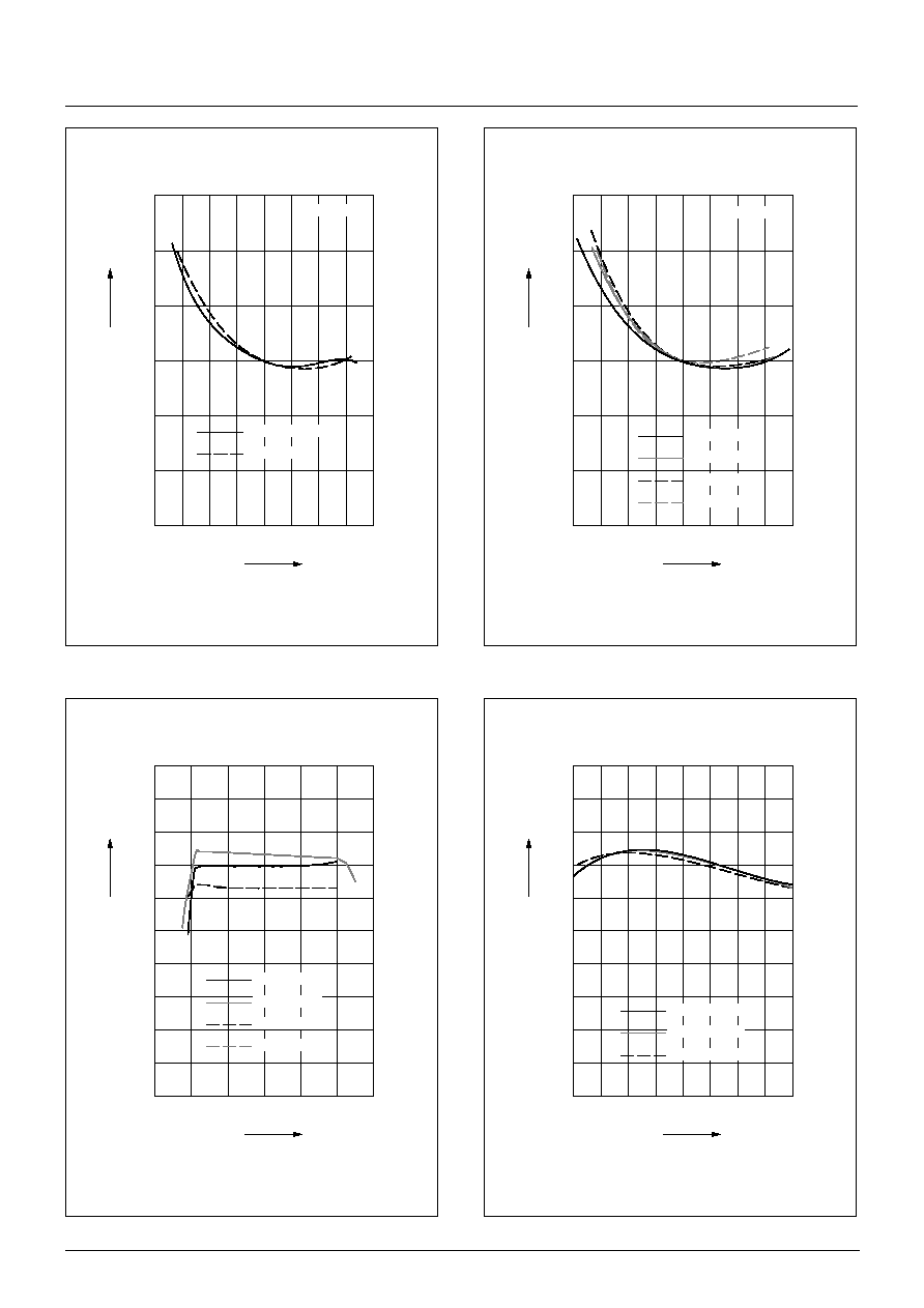
The normal integrating characteristics of a voltmeter is
sufficient for signal filtering.
Do not connect OUT1 or OUT2 to Ground.
V
DD
OUT1
OUT2
GND
HAL 401
Oscillo-
scope
Ch1
Ch2
Fig. 4≠1: Filtering of output signals
V
DD
1
2
3
4
330 p
330 p
4.7n
47 n
47 n
1 k
1 k
3.3 k
3.3 k
6.8 n
Display the difference between channel 1 and channel
2 to show the Hall voltage. Capacitors 4.7 nF and 330 pF
for electromagnetic immunity are recommended.
Do not connect OUT1 or OUT2 to Ground.
V
DD
OUT1
OUT2
GND
HAL 401
High
Low
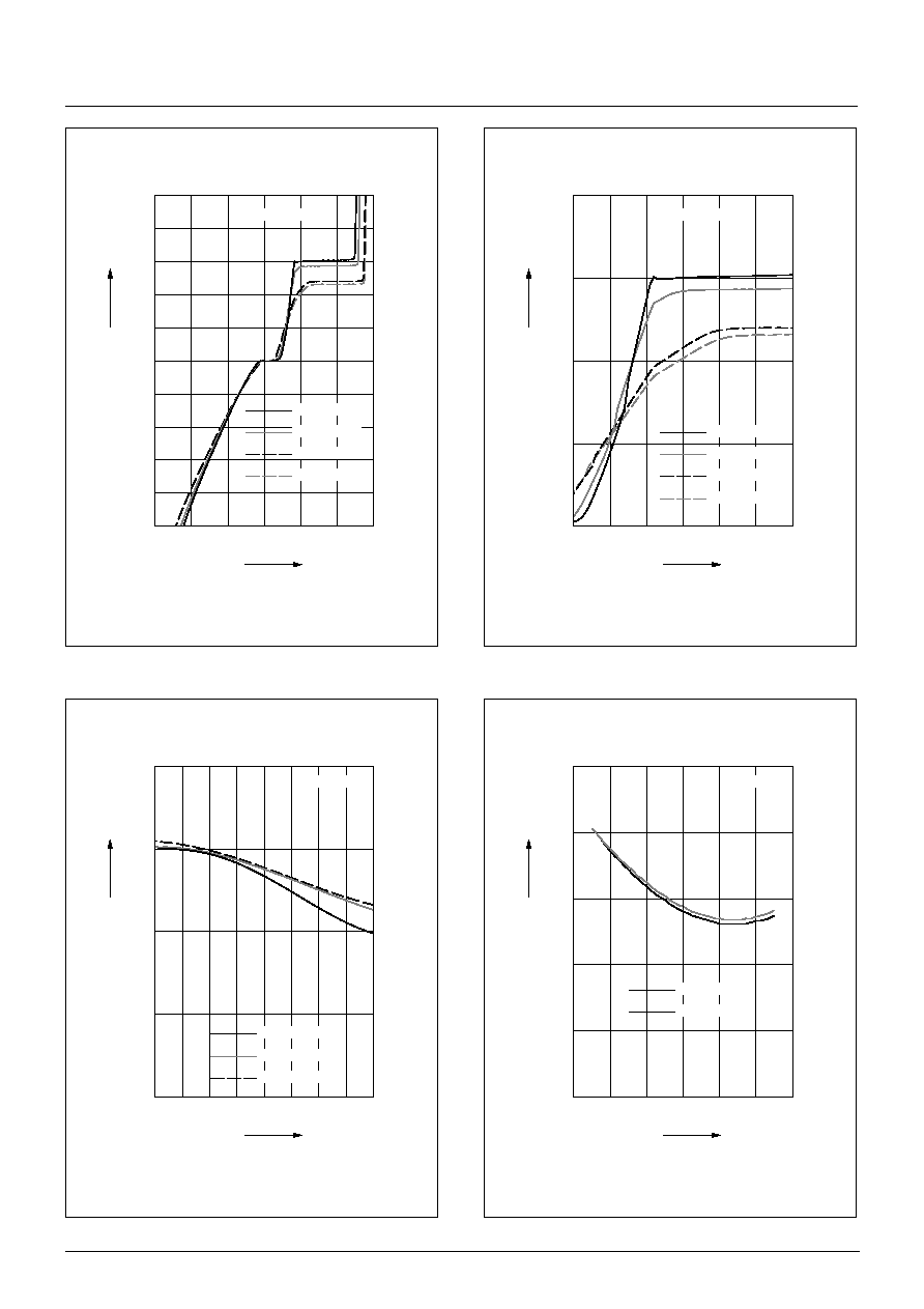
Fig. 4≠2: Flux density measurement with voltmeter
V
DD
1
2
3
4
Voltage
Meter

HAL401
DATA SHEET
Freigabe-Exemplar
15
Micronas
Do not connect OUT1 or OUT2 to Ground.
V
DD
OUT1
OUT2
GND
HAL 401
Fig. 4≠3: Differential HAL 40x output to single-ended output
R = 10 k
, C = 7.5 nF,
R for offset adjustment, BW
≠3dB
= 1.3 kHz
V
DD
1
2
3
4
330 p
330 p
4.7n
ADC
V
CC
R
1.5 R
R≠
R
R+
R
1.33 C
0.75 R
CMOS
OPV
0.22 R
4.4 C
3 C
+
≠
Do not connect OUT1 or OUT2 to Ground.
V
DD
OUT1
OUT2
GND
HAL 401
Fig. 4≠4: Differential HAL 401 output to single-ended output (referenced to ground), filter ≠ BW
≠3dB
= 14.7 kHz
V
DD
1
2
3
4
330 p
330 p
4.7 n
4.7 k
4.7 k
4.7 k
CMOS
OPV
+
≠
4.7 n
4.7 k
8.2 n
CMOS
OPV
+
≠
2.2 n
4.7 k
4.7 k
3.0 k
1 n
V
CC
y
6 V
V
EE
x*
6 V
OUT

HAL401
DATA SHEET
Freigabe-Exemplar
16
Micronas
5. Data Sheet History
1. Final Data Sheet: "HAL 401 Linear Hall Effect Sen-
sor IC", June 26, 2002, 6251-470-1DS.
First release of the final data sheet.
Micronas GmbH
Hans-Bunte-Strasse 19
D-79108 Freiburg (Germany)
P.O. Box 840
D-79008 Freiburg (Germany)
Tel. +49-761-517-0
Fax +49-761-517-2174
E-mail: docservice@micronas.com
Internet: www.micronas.com
Printed in Germany
Order No. 6251-470-1DS
All information and data contained in this data sheet are without any
commitment, are not to be considered as an offer for conclusion of a
contract, nor shall they be construed as to create any liability. Any new
issue of this data sheet invalidates previous issues. Product availability
and delivery are exclusively subject to our respective order confirma-
tion form; the same applies to orders based on development samples
delivered. By this publication, Micronas GmbH does not assume re-
sponsibility for patent infringements or other rights of third parties
which may result from its use.
Further, Micronas GmbH reserves the right to revise this publication
and to make changes to its content, at any time, without obligation to
notify any person or entity of such revisions or changes.
No part of this publication may be reproduced, photocopied, stored on
a retrieval system, or transmitted without the express written consent
of Micronas GmbH.