 | –≠–ª–µ–∫—Ç—Ä–æ–Ω–Ω—ã–π –∫–æ–º–ø–æ–Ω–µ–Ω—Ç: HAL54x | –°–∫–∞—á–∞—Ç—å:  PDF PDF  ZIP ZIP |
HAL54x
Hall Effect Sensor Family
Edition Nov. 27, 2002
6251-605-1DS
DATA SHEET
MICRONAS
MICRONAS

HAL54x
DATA SHEET
2
Nov. 27, 2002; 6251-605-1DS
Micronas
Contents
Page
Section
Title
3
1.
Introduction
3
1.1.
Features
3
1.2.
Family Overview
4
1.3.
Marking Code
4
1.3.1.
Special Marking of Prototype Parts
4
1.4.
Operating Junction Temperature Range
4
1.5.
Hall Sensor Package Codes
4
1.6.
Solderability
5
2.
Functional Description
6
3.
Specifications
6
3.1.
Outline Dimensions
6
3.2.
Dimensions of Sensitive Area
6
3.3.
Positions of Sensitive Areas
7
3.4.
Absolute Maximum Ratings
7
3.4.1.
Storage, Moisture Sensitivity Class and Shelf Life
7
3.5.
Recommended Operating Conditions
8
3.6.
Electrical Characteristics
9
3.7.
Magnetic Characteristics Overview
14
4.
Type Descriptions
14
4.1.
HAL542
16
4.2.
HAL543
18
4.3.
HAL546
20
4.4.
HAL548
22
5.
Application
22
5.1.
Ambient Temperature
22
5.2.
Extended Operating Conditions
22
5.3.
Start-up Behavior
22
5.4.
EMC and ESD
24
6.
Data Sheet History

DATA SHEET
HAL54x
Micronas
Nov. 27, 2002; 6251-605-1DS
3
Hall Effect Sensor Family
in CMOS technology
1. Introduction
The HAL 54x family consists of different Hall switches
produced in CMOS technology. All sensors include a
temperature-compensated Hall plate with active offset
compensation, a comparator, and an open-drain out-
put transistor. The comparator compares the actual
magnetic flux through the Hall plate (Hall voltage) with
the fixed reference values (switching points). Accord-
ingly, the output transistor is switched on or off.
In addition to the HAL50x/51x family, the HAL54x fea-
tures a power-on and undervoltage reset.
The sensors of this family differ in the switching behav-
ior and the switching points.
The active offset compensation leads to constant mag-
netic characteristics over supply voltage and tempera-
ture range. In addition, the magnetic parameters are
robust against mechanical stress effects.
The sensors are designed for industrial and automo-
tive applications and operate with supply voltages
from 4.3 V to 24 V in the ambient temperature range
from
-
40∞C up to 150∞C.
All sensors are available in a SMD-package (SOT89B)
and in a leaded version (TO-92UA).
1.1. Features
≠ switching offset compensation at typically 62 kHz
≠ operates from 4.3 V to 24 V supply voltage
≠ overvoltage protection at all pins
≠ reverse-voltage protection at V
DD
-pin
≠ magnetic characteristics are robust against
mechanical stress effects
≠ short-circuit protected open-drain output by thermal
shut down
≠ operates with static magnetic fields and dynamic
magnetic fields up to 10 kHz
≠ constant switching points over a wide supply volt-
age range
≠ the decrease of magnetic flux density caused by ris-
ing temperature in the sensor system is compen-
sated by a built-in negative temperature coefficient
of the magnetic characteristics
≠ ideal sensor for applications in extreme automotive
and industrial environments
1.2. Family Overview
The types differ according to the magnetic flux density
values for the magnetic switching points and the tem-
perature behavior of the magnetic switching points.
Latching Sensors:
The output turns low with the magnetic south pole on
the branded side of the package and turns high with
the magnetic north pole on the branded side. The out-
put does not change if the magnetic field is removed.
For changing the output state, the opposite magnetic
field polarity must be applied.
Unipolar Sensors:
The output turns low with the magnetic south pole on
the branded side of the package and turns high if the
magnetic field is removed. The sensor does not
respond to the magnetic north pole on the branded
side.
Type
Switching
Behavior
Sensitivity
see
Page
542
latching
high
14
543
unipolar
low
16
546
unipolar
high
18
548
unipolar
medium
20

HAL54x
DATA SHEET
4
Nov. 27, 2002; 6251-605-1DS
Micronas
1.3. Marking Code
All Hall sensors have a marking on the package sur-
face (branded side). This marking includes the name
of the sensor and the temperature range.
1.3.1. Special Marking of Prototype Parts
Prototype parts are coded with an underscore beneath
the temperature range letter on each IC. They may be
used for lab experiments and design-ins but are not
intended to be used for qualification tests or as produc-
tion parts.
1.4. Operating Junction Temperature Range
The Hall sensors from Micronas are specified to the
chip temperature (junction temperature T
J
).
K: T
J
=
-
40
∞
C to +140
∞
C
E: T
J
=
-
40
∞
C to +100
∞
C
Note: Due to the high power dissipation at high current
consumption, there is a difference between the
ambient temperature (T
A
) and junction tempera-
ture. Please refer to section 5.1. on page 22 for
details.
1.5. Hall Sensor Package Codes
Hall sensors are available in a wide variety of packag-
ing versions and quantities. For more detailed informa-
tion, please refer to the brochure: "Ordering Codes for
Hall Sensors".
1.6. Solderability
all packages: according to IEC68-2-58
During soldering reflow processing and manual
reworking, a component body temperature of 260
∞
C
should not be exceeded.
Components stored in the original packaging should
provide a shelf life of at least 12 months, starting from
the date code printed on the labels, even in environ-
ments as extreme as 40
∞
C and 90% relative humidity.
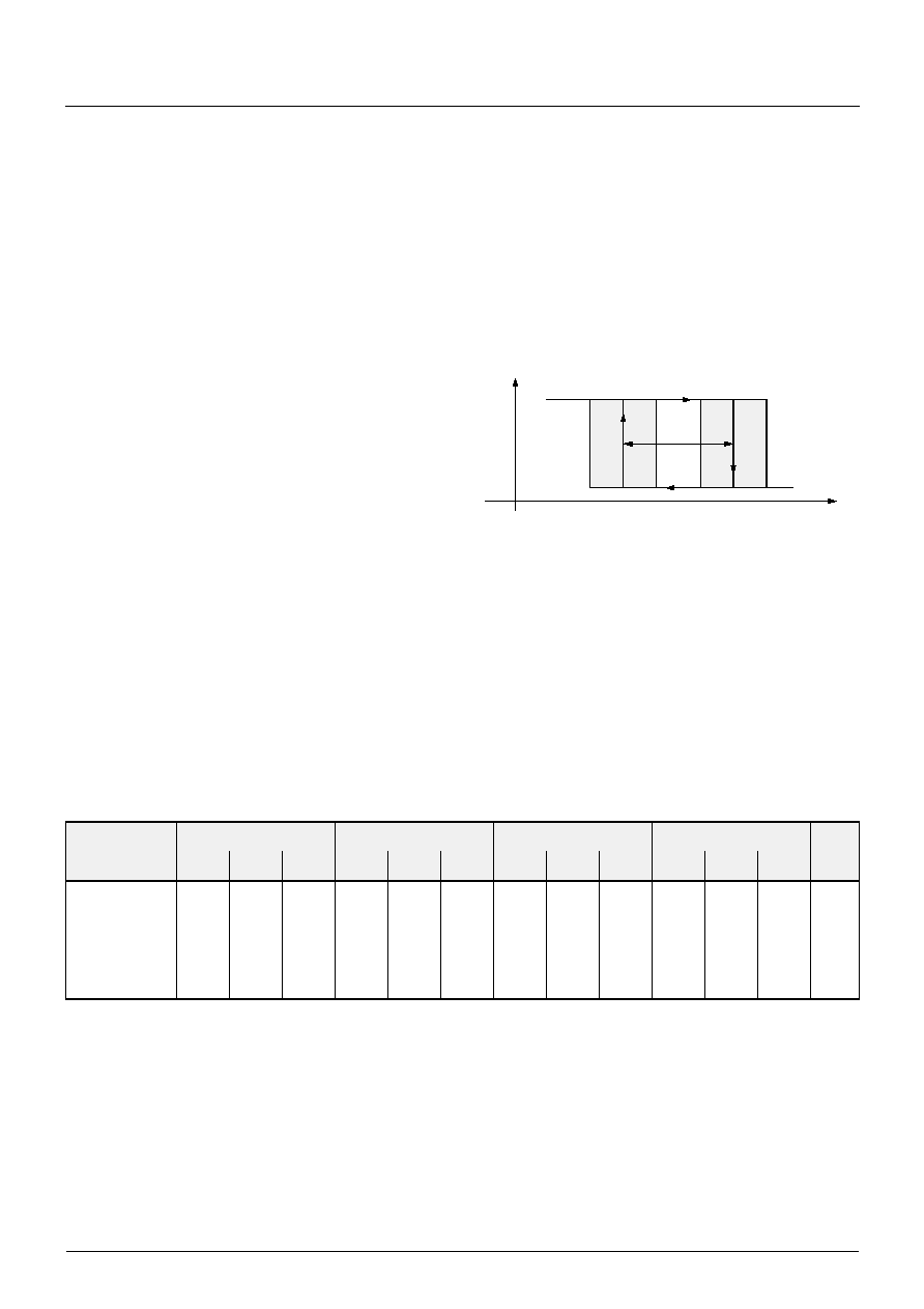
Fig. 1≠1: Pin configuration
Type
Temperature Range
K
E
HAL542
542K
542E
HAL543
543K
543E
HAL546
546K
546E
HAL548
548K
548E
HALXXXPA-T
Temperature Range: Kor E
Package: SF for SOT-89B
UA for TO-92UA
Type: 54x
Example: HAL542UA-K
Type: 542
Package: TO-92UA
Temperature Range: T
J
=
-
40
∞
C to +140
∞
C
1 V
DD
2
GND
3
OUT
DATA SHEET
HAL54x
Micronas
Nov. 27, 2002; 6251-605-1DS
5
2. Functional Description
The Hall effect sensor is a monolithic integrated circuit
that switches in response to magnetic fields. If a mag-
netic field with flux lines perpendicular to the sensitive
area is applied to the sensor, the biased Hall plate
forces a Hall voltage proportional to this field. The Hall
voltage is compared with the actual threshold level in
the comparator. The temperature-dependent bias
increases the supply voltage of the Hall plates and
adjusts the switching points to the decreasing induc-
tion of magnets at higher temperatures. If the magnetic
field exceeds the threshold levels, the open drain out-
put switches to the appropriate state. The built-in hys-
teresis eliminates oscillation and provides switching
behavior of output without bouncing.
Magnetic offset caused by mechanical stress is com-
pensated for by using the "switching offset compensa-
tion technique". Therefore, an internal oscillator pro-
vides a two phase clock. The Hall voltage is sampled
at the end of the first phase. At the end of the second
phase, both sampled and actual Hall voltages are
averaged and compared with the actual switching
point. Subsequently, the open drain output switches to
the appropriate state. The time from crossing the mag-
netic switching level to switching of output can vary
between zero and 1/f
osc
.
Shunt protection devices clamp voltage peaks at the
Output-pin and V
DD
-pin together with external series
resistors. Reverse current is limited at the V
DD
-pin by
an internal series resistor up to
-
15 V. No external
reverse protection diode is needed at the V
DD
-pin for
reverse voltages ranging from 0 V to
-
15 V.
A built-in reset-circuit clamps the output to the "high"
state (reset state) during power-on or when the supply
voltage drops below a reset voltage of V
reset
< 4.3 V.
For supply voltages between V
reset
and 4.3 V, the out-
put state of the device responds to the magnetic field.
For supply voltages above 4.3 V, the device works
according to the specified characteristics.
Fig. 2≠1: HAL54x block diagram
Fig. 2≠2: Timing diagram
HAL 54x
Temperature
Dependent
Bias
Switch
Hysteresis
Control
Comparator
Output
V
DD
1
OUT
3
Clock
Hall Plate
GND
2
Power-on &
Undervoltage
Reset
Short Circuit &
Overvoltage
Protection
Reverse
Voltage &
Overvoltage
Protection
t
V
OL
V
OUT
1/f
osc
= 9
µ
s
V
OH
B
B
ON
f
osc
t
t
t
f
t
I
DD
t

HAL54x
DATA SHEET
6
Nov. 27, 2002; 6251-605-1DS
Micronas
3. Specifications
3.1. Outline Dimensions
Fig. 3≠1:
Plastic Small Outline Transistor Package
(SOT-89B)
Weight approximately 0.035 g
Dimensions in mm
3.2. Dimensions of Sensitive Area
0.25 mm
◊
0.12 mm
3.3. Positions of Sensitive Areas
Fig. 3≠2:
Plastic Transistor Single Outline Package
(TO-92UA)
Weight approximately 0.12 g
Dimensions in mm
Note: For all package diagrams, a mechanical toler-
ance of
±
0.05 mm applies to all dimensions
where no tolerance is explicitly given. Package
dimensions exclude moulding flash.
SOT-89B
TO-92UA
x
center of
the package
center of
the package
y
0.95 mm nominal
1.0 mm nominal
4.55
1.7
min.
0.25
2.55
0.4
0.4
0.4
1.5
3.0
0.06
±
0.04
branded side
SPGS0022-5-A3/2E
y
1
2
3
4
±
0.2
0.15
0.3
2
0.2
sensitive area
top view
1.15
SPGS007002-11-A/1E
branded side

DATA SHEET
HAL54x
Micronas
Nov. 27, 2002; 6251-605-1DS
7
3.4. Absolute Maximum Ratings
Stresses beyond those listed in the "Absolute Maximum Ratings" may cause permanent damage to the device. This
is a stress rating only. Functional operation of the device at these or any other conditions beyond those indicated in
the "Recommended Operating Conditions/Characteristics" of this specification is not implied. Exposure to absolute
maximum ratings conditions for extended periods may affect device reliability.
3.4.1. Storage, Moisture Sensitivity Class, and Shelf Life
Storage has no influence on the electrical and magnetic characteristics of the sensors. However, under disadvanta-
geous conditions, extended storage time can lead to alteration of the lead plating, which affects the soldering pro-
cess.
Moisture Sensitivity Class: The package SOT-89B achieves level 1 according to J-STD-020A "Moisture/ Reflow
Sensitivity Classification for Non-hermetic Solid State Surface Mount Devices". If the sensors are stored at a maxi-
mum 30 ∞C and a maximum 90% relative humidity, no Dry Pack is required.
The permissible storage time (shelf life) of the sensors is a minimum of 12 months, starting from the date of manu-
facture, if they are stored in the original packaging at a maximum of 40 ∞C ambient temperature and a maximum of
90% relative humidity.
3.5. Recommended Operating Conditions
Symbol
Parameter
Pin Name
Min.
Max.
Unit
V
DD
Supply Voltage
1
-
15
28
1)
V
V
O
Output Voltage
3
-
0.3
28
1)
V
I
O
Continuous Output On Current
3
-
50
1)
mA
T
J
Junction Temperature Range
-
40
170
∞
C
1)
as long as T
J
max
is not exceeded
Symbol
Parameter
Pin Name
Min.
Max.
Unit
V
DD
Supply Voltage
1
4.3
24
V
I
O
Continuous Output On Current
3
0
20
mA
V
O
Output Voltage
(output switched off)
3
0
24
V

HAL54x
DATA SHEET
8
Nov. 27, 2002; 6251-605-1DS
Micronas
3.6. Electrical Characteristics at T
J
=
-
40
∞
C to +140
∞
C, V
DD
= 4.3 V to 24 V, as not otherwise specified in Conditions.
Typical Characteristics for T
J
= 25
∞
C and V
DD
= 12 V
Fig. 3≠3: Recommended pad size SOT-89B
Dimensions in mm
Symbol
Parameter
Pin No.
Min.
Typ.
Max.
Unit
Conditions
I
DD
Supply Current
1
2.3
3
4.2
mA
T
J
= 25
∞
C
I
DD
Supply Current over
Temperature Range
1
1.6
3
5.2
mA
V
DDZ
Overvoltage Protection
at Supply
1
-
28.5
32
V
I
DD
= 25 mA,
T
J
= 25
∞
C,
t = 20 ms
V
OZ
Overvoltage Protection at Output
3
-
28
32
V
I
OH
= 25 mA,
T
J
= 25
∞
C,
t = 20 ms
V
OL
Output Voltage
3
-
130
280 mV
I
OL
= 20 mA, T
J
= 25
∞
C
V
OL
Output Voltage over
Temperature Range
3
-
130
400 mV
I
OL
= 20 mA
I
OH
Output Leakage Current
3
-
0.06
0.1
µ
A
Output switched off,
T
J
= 25
∞
C, V
OH
= 4.3 to 24 V
I
OH
Output Leakage Current over
Temperature Range
3
-
-
10
µ
A
Output switched off,
T
J
150
∞
C, V
OH
= 4.3 to 24V
f
osc
Internal Oscillator
Chopper Frequency
-
-
62
-
kHz
T
J
= 25
∞
C,
V
DD
= 4.5 to 24 V
V
reset
Reset Voltage
1
-
3.8
-
V
t
en(O)
Enable Time of Output after
Setting of V
DD
1
-
70
-
µ
s
V
DD
= 12 V
2)
t
r
Output Rise Time
3
-
75
400
ns
V
DD
= 12 V,
R
L
= 820 Ohm,
C
L
= 20 pF
t
f
Output Fall Time
3
-
50
400
ns
R
thJSB
case
SOT-89B
Thermal Resistance Junction
to Substrate Backside
-
-
150
200
K/W
Fiberglass Substrate
30 mm x 10 mm x 1.5 mm,
pad size (see Fig. 3≠3)
R
thJA
case
TO-92UA
Thermal Resistance Junction
to Soldering Point
-
-
150
200
K/W
2)
B > B
ON
+ 2 mT or B < B
OFF
- 2 mT
5.0
2.0
2.0
1.0

DATA SHEET
HAL54x
Micronas
Nov. 27, 2002; 6251-605-1DS
9
3.7. Magnetic Characteristics Overview at T
J
=
-
40
∞
C to +140
∞
C, V
DD
= 4.3 V to 24 V,
Typical Characteristics for V
DD
= 12 V
Magnetic flux density values of switching points.
Positive flux density values refer to the magnetic south pole at the branded side of the package.
Note: For detailed descriptions of the individual types, see pages 14 and following.
Sensor
Parameter
On point B
ON
Off point B
OFF
Hysteresis B
HYS
Unit
Switching Type
T
J
Min.
Typ.
Max.
Min.
Typ.
Max.
Min.
Typ.
Max.
HAL542
-
40
∞
C
1
2.8
5
-
5
-
2.8
-
1
4.5
5.85
7.2
mT
latching
25
∞
C
1
2.6
4.5
-
4.5
-
2.6
-
1
4.5
5.5
6.5
mT
140
∞
C
0.5
2.3
4.8
-
4.8
-
2.3
-
0.5
3.0
4.0
6.0
mT
HAL543
-
40
∞
C
21
27
33
15
21
27
4
6
8
mT
unipolar
25
∞
C
21
27
33
15
21
27
4
6
8
mT
140
∞
C
21
26
33
15
20
27
4
5.5
8
mT
HAL546
-
40
∞
C
4.3
5.9
7.7
2.1
3.8
5.5
1.5
2.1
2.9
mT
unipolar
25
∞
C
3.8
5.5
7.2
2
3.5
5
1.4
2
2.8
mT
140
∞
C
3.2
4.8
6.9
1.8
3.1
5.5
1
1.7
2.6
mT
HAL548
-
40
∞
C
12
19
24
6
13
18
4
6.2
8
mT
unipolar
25
∞
C
12
18
24
6
12
18
4
5.6
8
mT
140
∞
C
12
16
24
6
11
18
4
5
8
mT

HAL54x
DATA SHEET
10
Nov. 27, 2002; 6251-605-1DS
Micronas
≠15
≠10
≠5
0
5
10
15
20
≠15≠10 ≠5 0
5
10 15 20 25 30 35 V
mA
V
DD
I
DD
T
A
= ≠40
∞
C
T
A
= 25
∞
C
T
A
=140
∞
C
25
HAL 54x
Fig. 3≠4: Typical supply current
versus supply voltage
0
0.5
1.0
1.5
2.0
2.5
3.0
3.5
4.0
4.5
5.0
1
2
3
4
5
6
7
8 V
mA
V
DD
I
DD
T
A
= ≠40
∞
C
T
A
= 25
∞
C
T
A
= 140
∞
C
T
A
= 100
∞
C
HAL 54x
Fig. 3≠5: Typical supply current
versus supply voltage
0
1
2
3
4
5
≠50
0
50
100
150
200
∞
C
mA
T
A
I
DD
V
DD
= 3.8 V
V
DD
= 12 V
V
DD
= 24 V
HAL 54x
Fig. 3≠6: Typical supply current
versus ambient temperature
0
10
20
30
40
50
60
70
80
90
100
≠50
0
50
100
150
200
∞
C
kHz
T
A
f
osc
V
DD
= 3.8 V
V
DD
= 4.5 V...24 V
HAL 54x
Fig. 3≠7: Typ. internal chopper frequency
versus ambient temperature

DATA SHEET
HAL54x
Micronas
Nov. 27, 2002; 6251-605-1DS
11
0
10
20
30
40
50
60
70
80
90
100
0
5
10
15
20
25
30 V
kHz
V
DD
f
osc
T
A
= ≠40
∞
C
T
A
= 25
∞
C
T
A
= 140
∞
C
HAL 54x
Fig. 3≠8: Typ. internal chopper frequency
versus supply voltage
0
10
20
30
40
50
60
70
80
90
100
3
3.5
4.0
4.5
5.0
5.5
6.0 V
kHz
V
DD
f
osc
T
A
= ≠40
∞
C
T
A
= 25
∞
C
T
A
= 140
∞
C
HAL 54x
Fig. 3≠9: Typ. internal chopper frequency
versus supply voltage
0
50
100
150
200
250
300
350
0
5
10
15
20
25
30 V
mV
V
DD
V
OL
T
A
= ≠40
∞
C
T
A
= 25
∞
C
I
O
= 20 mA
T
A
= 100
∞
C
HAL 54x
Fig. 3≠10: Typical output low voltage
versus supply voltage
0
100
200
300
400
≠50
0
50
100
150
200
∞
C
mV
T
A
V
OL
V
DD
= 24 V
V
DD
= 3.8 V
V
DD
= 4.5 V
HAL 54x
I
O
= 20 mA
Fig. 3≠11: Typical output low voltage
versus ambient temperature

HAL54x
DATA SHEET
12
Nov. 27, 2002; 6251-605-1DS
Micronas
15
20
25
30
35 V
V
OH
I
OH
T
A
= ≠40
∞
C
T
A
= 150
∞
C
T
A
= 100
∞
C
T
A
= 25
∞
C
10
≠6
10
≠5
10
≠4
10
≠3
10
≠2
10
≠1
10
0
10
1
10
2
10
3
10
4
HAL 54x
µ
A
Fig. 3≠12: Typ. output high current
versus output voltage
≠50
0
50
100
150
200
∞
C
µ
A
T
A
I
OH
V
OH
= 24 V
V
OH
= 3.8 V
10
≠5
10
≠4
10
≠3
10
≠2
10
≠1
10
0
10
1
10
2
HAL 54x
Fig. 3≠13: Typical output leakage current
versus ambient temperature
≠30
≠20
≠10
0
10
20
30
0.01
0.10
1.00
10.00 100.00 1000.00
dB
µ
A
f
I
DD
V
DD
= 12 V
T
A
= 25
∞
C
Quasi-Peak-
Measurement
HAL 54x
max. spurious
signals
1
10
100
1000 MHz
Fig. 3≠14: Typ. spectrum of supply current
0
10
20
30
40
50
60
70
80
0.01
0.10
1.00
10.00 100.00 1000.00
dB
µ
V
f
V
DD
V
P
= 12 V
T
A
= 25
∞
C
Quasi-Peak-
Measurement
test circuit 2
HAL 54x
max. spurious
signals
1
10
100
1000 MHz
Fig. 3≠15: Typ. spectrum of supply voltage

DATA SHEET
HAL54x
Micronas
Nov. 27, 2002; 6251-605-1DS
13
LQWHQWLRQDOO\ OHIW YDFDQW

HAL542
DATA SHEET
14
Nov. 27, 2002; 6251-605-1DS
Micronas
4. Type Descriptions
4.1. HAL542
The HAL542 is the most sensitive latching sensor of
this family (see Fig. 4≠1).
The output turns low with the magnetic south pole on
the branded side of the package and turns high with
the magnetic north pole on the branded side. The out-
put does not change if the magnetic field is removed.
For changing the output state, the opposite magnetic
field polarity must be applied.
For correct functioning in the application, the sensor
requires both magnetic polarities (north and south) on
the branded side of the package.
Magnetic Features:
≠ switching type: latching
≠ high sensitivity
≠ typical B
ON
: 2.6 mT at room temperature
≠ typical B
OFF
:
-
2.6 mT at room temperature
≠ operates with static magnetic fields and dynamic
magnetic fields up to 10 kHz
≠ typical temperature coefficient of magnetic switching
points is
-
1000 ppm/K
Applications
The HAL542 is the optimal sensor for applications with
alternating magnetic signals and weak magnetic
amplitude at the sensor position such as:
≠ applications with large airgap or weak magnets,
≠ rotating speed measurement,
≠ commutation of brushless DC motors, and
≠ CAM shaft sensors, and
≠ magnetic encoders.
Fig. 4≠1: Definition of magnetic switching points for
the HAL542
Magnetic Characteristics at T
J
=
-
40
∞
C to +140
∞
C, V
DD
= 4.3 V to 24 V,
Typical Characteristics for V
DD
= 12 V
Magnetic flux density values of switching points.
Positive flux density values refer to the magnetic south pole at the branded side of the package.
The hysteresis is the difference between the switching points B
HYS
= B
ON
-
B
OFF
The magnetic offset is the mean value of the switching points B
OFFSET
= (B
ON
+ B
OFF
) / 2
B
OFF
B
ON
0
V
OL
V
O
Output Voltage
B
B
HYS
Parameter
On point B
ON
Off point B
OFF
Hysteresis B
HYS
Magnetic Offset
Unit
T
J
Min.
Typ.
Max.
Min.
Typ.
Max.
Min.
Typ.
Max.
Min.
Typ.
Max.
-
40
∞
C
1
2.8
5
-
5
-
2.8
-
1
4.5
5.85
7.2
0
mT
25
∞
C
1
2.6
4.5
-
4.5
-
2.6
-
1
4.5
5.5
6.5
-
1.5
0
1.5
mT
100
∞
C
0.95
2.5
4.4
-
4.4
-
2.5
-
0.95
3.7
5.0
6.3
0
mT
140
∞
C
0.6
2.4
4.6
-
4.6
-
2.4
-
0.6
3.3
4.8
6.2
0
mT

DATA SHEET
HAL542
Micronas
Nov. 27, 2002; 6251-605-1DS
15
Note: In the diagram "Magnetic switching points ver-
sus ambient temperature", the curves for
B
ON
min, B
ON
max, B
OFF
min, and B
OFF
max
refer to junction temperature, whereas typical
curves refer to ambient temperature.
≠6
≠4
≠2
0
2
4
6
0
5
10
15
20
25
30 V
mT
V
DD
B
ON
B
OFF
HAL 542
B
ON
B
OFF
T
A
= ≠40
∞
C
T
A
= 25
∞
C
T
A
= 140
∞
C
T
A
= 100
∞
C
Fig. 4≠2: Typ. magnetic switching points
versus supply voltage
≠6
≠4
≠2
0
2
4
6
≠50
0
50
100
150
200
∞
C
mT
T
A
, T
J
B
ON
B
OFF
V
DD
= 3.8 V
V
DD
= 4.3 V... 24 V
B
ON
max
B
ON
typ
B
ON
min
B
OFF
max
B
OFF
typ
B
OFF
min
HAL 542
Fig. 4≠3: Magnetic switching points
versus temperature
HAL543
DATA SHEET
16
Nov. 27, 2002; 6251-605-1DS
Micronas
4.2. HAL543
The HAL543 is the most insensitive unipolar sensor of
this family (see Fig. 4≠4).
The output turns low with the magnetic south pole on
the branded side of the package and turns high if the
magnetic field is removed. The sensor does not
respond to the magnetic north pole on the branded
side.
Magnetic Features:
≠ switching type: unipolar
≠ low sensitivity
≠ typical B
ON
: 27 mT at room temperature
≠ typical B
OFF
: 21 mT at room temperature
≠ operates with static magnetic fields and dynamic
magnetic fields up to 10 kHz
Applications
The HAL543 is the optimal sensor for applications with
unipolar magnetic signals and large magnetic ampli-
tude at the sensor position such as:
≠ position and end point detection,
≠ contactless solution to replace micro switches,
≠ rotating speed measurement.
Fig. 4≠4: Definition of magnetic switching points for
the HAL543
Magnetic Characteristics at T
J
=
-
40
∞
C to +140
∞
C, V
DD
= 4.3 V to 24 V,
Typical Characteristics for V
DD
= 12 V
Magnetic flux density values of switching points.
Positive flux density values refer to the magnetic south pole at the branded side of the package.
The hysteresis is the difference between the switching points B
HYS
= B
ON
-
B
OFF
The magnetic offset is the mean value of the switching points B
OFFSET
= (B
ON
+ B
OFF
) / 2
B
OFF
B
ON
0
V
OL
V
O
Output Voltage
B
B
HYS
Parameter
On point B
ON
Off point B
OFF
Hysteresis B
HYS
Magnetic Offset
Unit
T
J
Min.
Typ.
Max.
Min.
Typ.
Max.
Min.
Typ.
Max.
Min.
Typ.
Max.
-
40
∞
C
21
27
33
15
21
27
4
6
8
-
24
-
mT
25
∞
C
21
27
33
15
21
27
4
6
8
18
24
30
mT
100
∞
C
21
27
33
15
21
27
4
6
8
-
24
-
mT
140
∞
C
21
27
33
15
21
27
4
5.5
8
-
24
-
mT
DATA SHEET
HAL543
Micronas
Nov. 27, 2002; 6251-605-1DS
17
Note: In the diagram "Magnetic switching points ver-
sus ambient temperature", the curves for
B
ON
min, B
ON
max, B
OFF
min, and B
OFF
max
refer to junction temperature, whereas typical
curves refer to ambient temperature.
10
12
14
16
18
20
22
24
26
28
30
0
5
10
15
20
25
30 V
mT
V
DD
B
ON
B
OFF
HAL 543
B
OFF
T
A
= ≠40
∞
C
T
A
= 25
∞
C
T
A
= 140
∞
C
T
A
= 100
∞
C
B
ON
Fig. 4≠5: Typ. magnetic switching points
versus supply voltage
10
15
20
25
30
35
40
≠50
0
50
100
150
200
∞
C
mT
T
A
, T
J
B
ON
B
OFF
V
DD
= 4.3 V... 24 V
B
ON
max
B
ON
typ
B
ON
min
B
OFF
max
B
OFF
typ
B
OFF
min
HAL 543
Fig. 4≠6: Magnetic switching points
versus temperature

HAL546
DATA SHEET
18
Nov. 27, 2002; 6251-605-1DS
Micronas
4.3. HAL546
The HAL546 is a quite sensitive unipolar sensor (see
Fig. 4≠7).
The output turns low with the magnetic south pole on
the branded side of the package and turns high if the
magnetic field is removed. The sensor does not
respond to the magnetic north pole on the branded
side.
Magnetic Features:
≠ switching type: unipolar
≠ high sensitivity
≠ typical B
ON
: 5.5 mT at room temperature
≠ typical B
OFF
: 3.5 mT at room temperature
≠ operates with static magnetic fields and dynamic
magnetic fields up to 10 kHz
≠ typical temperature coefficient of magnetic switching
points is
-
1000 ppm/K.
Applications
The HAL546 is the optimal sensor for applications with
one magnetic polarity such as:
≠ solid state switches,
≠ contactless solution to replace micro-switches, and
≠ rotating speed measurement.
Fig. 4≠7: Definition of magnetic switching points for
the HAL546
Magnetic Characteristics at T
J
=
-
40
∞
C to +140
∞
C, V
DD
= 4.3 V to 24 V,
Typical Characteristics for V
DD
= 12 V
Magnetic flux density values of switching points.
Positive flux density values refer to the magnetic south pole at the branded side of the package.
The hysteresis is the difference between the switching points B
HYS
= B
ON
-
B
OFF
The magnetic offset is the mean value of the switching points B
OFFSET
= (B
ON
+ B
OFF
) / 2
B
OFF
B
ON
0
V
OL
V
O
Output Voltage
B
B
HYS
Parameter
On point B
ON
Off point B
OFF
Hysteresis B
HYS
Magnetic Offset
Unit
T
J
Min.
Typ.
Max.
Min.
Typ.
Max.
Min.
Typ.
Max.
Min.
Typ.
Max.
-
40
∞
C
4.3
5.9
7.7
2.1
3.8
5.5
1.5
2.1
2.9
-
4.9
-
mT
25
∞
C
3.8
5.5
7.2
2
3.5
5
1.4
2
2.8
2.9
4.5
6.1
mT
100
∞
C
3.5
5.3
7
1.9
3.3
5.4
1.1
1.9
2.6
-
4.3
-
mT
140
∞
C
3.2
4.8
6.9
1.8
3.1
5.5
1
1.7
2.6
-
4
-
mT

DATA SHEET
HAL546
Micronas
Nov. 27, 2002; 6251-605-1DS
19
Note: In the diagram "Magnetic switching points ver-
sus ambient temperature", the curves for
B
ON
min, B
ON
max, B
OFF
min, and B
OFF
max
refer to junction temperature, whereas typical
curves refer to ambient temperature.
0
1
2
3
4
5
6
7
8
0
5
10
15
20
25
30 V
mT
V
DD
B
ON
B
OFF
HAL 546
B
ON
B
OFF
T
A
= ≠40
∞
C
T
A
= 25
∞
C
T
A
= 140
∞
C
T
A
= 100
∞
C
Fig. 4≠8: Typ. magnetic switching points
versus supply voltage
0
1
2
3
4
5
6
7
8
≠50
0
50
100
150
200
∞
C
mT
T
A
, T
J
B
ON
B
OFF
V
DD
= 4.3 V... 24 V
B
ON
max
B
ON
typ
B
ON
min
B
OFF
max
B
OFF
typ
B
OFF
min
HAL 546
Fig. 4≠9: Magnetic switching points
versus temperature
HAL548
DATA SHEET
20
Nov. 27, 2002; 6251-605-1DS
Micronas
4.4. HAL548
The HAL 548 is a unipolar switching sensor (see
Fig. 4≠10).
The output turns low with the magnetic south pole on
the branded side of the package and turns high if the
magnetic field is removed. The sensor does not
respond to the magnetic north pole on the branded
side.
Magnetic Features:
≠ switching type: unipolar,
≠ medium sensitivity
≠ typical B
ON
:
18
mT at room temperature
≠ typical B
OFF
: 12
mT at room temperature
≠ operates with static magnetic fields and dynamic
magnetic fields up to 10 kHz
Applications
The HAL 548 is the ideal sensor for all applications
with one magnetic polarity and weak magnetic ampli-
tude at the sensor position such as:
≠ solid state switches,
≠ contactless solution to replace micro switches,
≠ position and end point detection, and
≠ rotating speed measurement.
Fig. 4≠10: Definition of magnetic switching points for
the HAL548
Magnetic Characteristics at T
J
=
-
40
∞
C to +140
∞
C, V
DD
= 4.3 V to 24 V,
Typical Characteristics for V
DD
= 12 V
Magnetic flux density values of switching points.
Positive flux density values refer to the magnetic south pole at the branded side of the package.
The hysteresis is the difference between the switching points B
HYS
= B
ON
-
B
OFF
The magnetic offset is the mean value of the switching points B
OFFSET
= (B
ON
+ B
OFF
) / 2
B
OFF
B
ON
0
V
OL
V
O
Output Voltage
B
B
HYS
Parameter
On point B
ON
Off point B
OFF
Hysteresis B
HYS
Magnetic Offset
Unit
T
J
Min.
Typ.
Max.
Min.
Typ.
Max.
Min.
Typ.
Max.
Min.
Typ.
Max.
-
40
∞
C
12
19
24
6
13
18
4
6
8
-
16
-
mT
25
∞
C
12
18
24
6
12
18
4
6
8
9
15
21
mT
100
∞
C
12
18
24
6
12
18
4
6
8
-
15
-
mT
140
∞
C
12
17
24
6
11
18
4
6
8
-
14
-
mT

DATA SHEET
HAL548
Micronas
Nov. 27, 2002; 6251-605-1DS
21
Note: In the diagram "Magnetic switching points ver-
sus ambient temperature", the curves for
B
ON
min, B
ON
max, B
OFF
min, and B
OFF
max
refer to junction temperature, whereas typical
curves refer to ambient temperature.
4
6
8
10
12
14
16
18
20
0
5
10
15
20
25
30 V
mT
V
DD
B
ON
B
OFF
HAL 548
B
ON
B
OFF
T
A
= ≠40
∞
C
T
A
= 25
∞
C
T
A
= 140
∞
C
T
A
= 100
∞
C
Fig. 4≠11: Typ. magnetic switching points
versus supply voltage
0
5
10
15
20
25
30
≠50
0
50
100
150
200
∞
C
mT
T
A
, T
J
B
ON
B
OFF
V
DD
= 4.3 V... 24 V
B
ON
max
B
ON
typ
B
ON
min
B
OFF
max
B
OFF
typ
B
OFF
min
HAL 548
Fig. 4≠12: Magnetic switching points
versus temperature

HAL54x
DATA SHEET
22
Nov. 27, 2002; 6251-605-1DS
Micronas
5. Application
5.1. Ambient Temperature
Due to the internal power dissipation, the temperature
on the silicon chip (junction temperature T
J
) is higher
than the temperature outside the package (ambient
temperature T
A
).
T
J
= T
A
+
T
Under static conditions and continuous operation, the
following equation applies:
T = I
DD
* V
DD
* R
th
For typical values, use the typical parameters. For
worst case calculation, use the max. parameters for
I
DD
and R
th
, and the max. value for V
DD
from the appli-
cation.
For all sensors, the junction temperature range T
J
is
specified. The maximum ambient temperature T
Amax
can be calculated as:
T
Amax
= T
Jmax
-
T
5.2. Extended Operating Conditions
All sensors fulfill the electrical and magnetic character-
istics when operated within the Recommended Oper-
ating Conditions (see page 8).
Supply Voltage Below 4.3 V
The devices contain a Power-on Reset (POR) and a
undervoltage reset. For V
dd
< V
reset
the output state is
high. For Vreset < Vdd < 4.3 V the device responds to
the magnetic field according to the specified magnetic
characteristics.
5.3. Start-up Behavior
Due to the active offset compensation, the sensors
have an initialization time (enable time t
en(O)
) after
applying the supply voltage. The parameter t
en(O)
is
specified in the Electrical Characteristics (see page 9).
During the initialization time, the output state for the
HAL54x is 'Off-state' (i.e. Output High). After t
en(O)
, the
output will be high. The output will be switched to low if
the applied magnetic field B is above B
ON
.
5.4. EMC and ESD
For applications with disturbances on the supply line or
radiated disturbances, a series resistor and a capacitor
are recommended (see Fig. 5≠1). The series resistor
and the capacitor should be placed as closely as pos-
sible to the Hall sensor.
Please contact Micronas for the detailed investigation
reports with the EMC and ESD results.
Fig. 5≠1: Test circuit for EMC investigations
WARNING:
DO NOT USE THESE SENSORS IN LIFE-
SUPPORTING SYSTEMS, AVIATION, AND
AEROSPACE APPLICATIONS.
R
V
220
V
EMC
V
P
4.7 nF
V
DD
OUT
GND
1
2
3
R
L
1.2 k
20 pF

DATA SHEET
HAL54x
Micronas
Nov. 27, 2002; 6251-605-1DS
23

All information and data contained in this data sheet are without any
commitment, are not to be considered as an offer for conclusion of a
contract, nor shall they be construed as to create any liability. Any new
issue of this data sheet invalidates previous issues. Product availability
and delivery are exclusively subject to our respective order confirmation
form; the same applies to orders based on development samples deliv-
ered. By this publication, Micronas GmbH does not assume responsibil-
ity for patent infringements or other rights of third parties which may
result from its use.
Further, Micronas GmbH reserves the right to revise this publication
and to make changes to its content, at any time, without obligation to
notify any person or entity of such revisions or changes.
No part of this publication may be reproduced, photocopied, stored on a
retrieval system, or transmitted without the express written consent of
Micronas GmbH.
HAL54x
DATA SHEET
24
Nov. 27, 2002; 6251-605-1DS
Micronas
Micronas GmbH
Hans-Bunte-Strasse 19
D-79108 Freiburg (Germany)
P.O. Box 840
D-79008 Freiburg (Germany)
Tel. +49-761-517-0
Fax +49-761-517-2174
E-mail: docservice@micronas.com
Internet: www.micronas.com
Printed in Germany
Order No. 6251-605-1DS
6. Data Sheet History
1. Data Sheet: "HAL54x Hall Effect Sensor Family",
Nov. 27, 2002, 6251-605-1DS. First release of the
data sheet.